Abstract
Strong electric fields are generated by radio frequency (RF) plasma sources, and though the RF portion is too high a frequency for ions to react, the direct current (DC) portion of these fields has been shown to cause the atomic migration of metals, which can influence film morphology even downstream of the plasma where ionized plasma species are absent. In particular, we have observed the growth of nanopillars due to metal atoms migrating toward the positive field of the remote plasma. A biased grid placed between the plasma and the substrate can shield the substrate from these fields so that, when grounded, smooth films can be grown to a root mean square roughness of less than 1 nm. Positively biasing the grid returns the growth of nanocolumns. Interestingly, negatively biasing the grid significantly reduced the carbon and hydrocarbon content of gallium nitride films grown at a low temperature (~660 °C) using a nitrogen plasma, as observed using secondary ion mass spectroscopy (SIMS) and optical absorption measurements. The films also showed a notable improvement in conductivity and visible appearance.
1. Introduction
GaN is a critical component of blue, green and white light-emitting diodes, as well as other devices, and is typically grown by metalorganic chemical vapor deposition (MOCVD) at temperatures around 1050 °C [1]. At this temperature, sapphire substrates are commonly used, but there is an incentive to grow GaN at lower temperatures to allow access to other, more temperature-sensitive substrates, such as ZnO, which is closely lattice-matched to GaN [2]. As explained below, one of the difficulties with this is that carbon contamination from metalorganics becomes greater at lower growth temperatures. In this work, we show a novel means of carbon reduction that can be used in some plasma-based systems.
We used a grid placed between a remote plasma and a substrate to obtain the carbon reduction. Grids are generally used in plasma systems to control ion and electron fluxes; however, for the work described here, the plasma is remote, so that ion and electron concentrations are minimal in the region of the substrate. For this case, the electric field of the grid is not for ion or electron flux control; instead, we are using the grid to observe and control metal electromigration. Electromigration effects have been observed for decades in liquid-phase epitaxy systems when using a technique called electroepitaxy, whereby an electric field is applied across an electrically conductive liquid metal melt [3,4].
In our previous work on the remote plasma-related deposition of GaN and InN, we observed electromigration effects somewhat similar to those seen with electroepitaxy, and we were able to demonstrate the effectiveness of a biased grid placed between a substrate and a remote plasma for controlling film morphology [5]. In particular, nanocolumns were observed to grow in the electric field generated by the plasma without the grid, but these were absent when the substrate was shielded by the grounded grid. There are a few other publications in which it has been observed that nanostructures align in electric fields during plasma growth [6,7,8], including some work on graphene [9,10]. Interestingly, subsequent to our own work [5], Qi et al. [10] used a Faraday cage to similarly shield their plasma-grown graphene from electric fields so that it would grow in a horizontal plane rather than the vertical plane induced by the fields.
The electric field alignment of nanostructures in direct plasma deposition systems appears to be poorly understood, partly because the ionized plasma species tend to have a dominant influence during film growth. However, the remote plasma environment used here allows some of these more subtle effects to be studied without the interference of ions or electrons.
Here, we report on unexpected results achieved when biasing the grid to a value of –50 V, for which we saw a significant reduction in carbon and hydrocarbon incorporation for GaN films grown at about 650 °C. The mechanism by which this occurs is currently unknown to us and will require further investigations, though we provide some speculation as to the potential source. Here, we provide details related to the growth conditions used as well as the methods of film analysis. We also provide some comparative growth data at the same growth temperature without the grid, which shows a gallium-rich material with carbon and hydrocarbon impurities. The samples produced for this study were examined with a number of techniques, including X-ray photoelectron spectroscopy (XPS), optical transmission measurements, scanning electron microscopy (SEM), atomic force microscopy (AFM) and X-ray diffraction. Secondary ion mass spectroscopy (SIMS) was also used. SIMS is a technique used to examine small impurity levels within a host matrix.
2. Materials and Methods
Figure 1 below provides a schematic diagram of the deposition system used for this study. The radiofrequency (RF) plasma source, despite being a remote plasma source, caused a direct current (DC) floating potential of +78 V at 4 cm above the substrate, where the grid was eventually placed. This positive potential was enough to cause the spontaneous growth of nanostructures under a wide range of operating conditions due to electrostatic attraction, which caused the migration of deposited metal atoms upward toward this positive field. An example is shown in the SEM image of Figure 2. We have separately reported on the nanostructures grown [5,11,12,13,14]. Grounding the grid above the substrate suppressed the positive potential that was acting upon the deposited film species and effectively stopped the formation of these nanostructures. Meanwhile, biasing the grid to +78 V allowed the nanostructures to form as per the case without the grid.
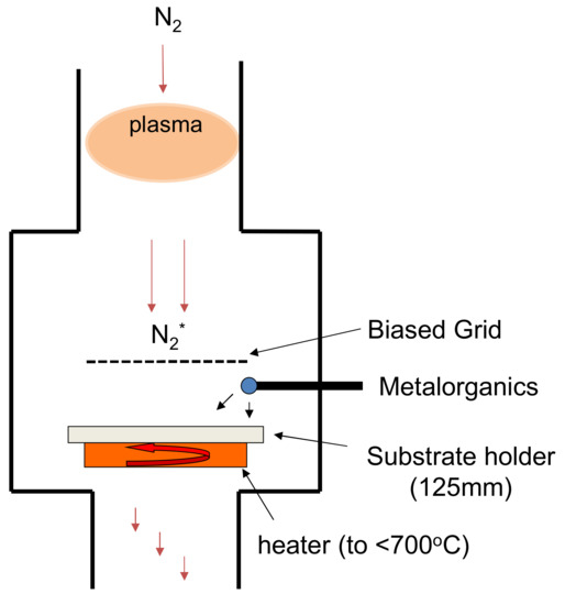
Figure 1.
Schematic diagram of the plasma system used for GaN film deposition. The substrate is located 125 mm away from the plasma source; the grid is 40 mm above the substrate.
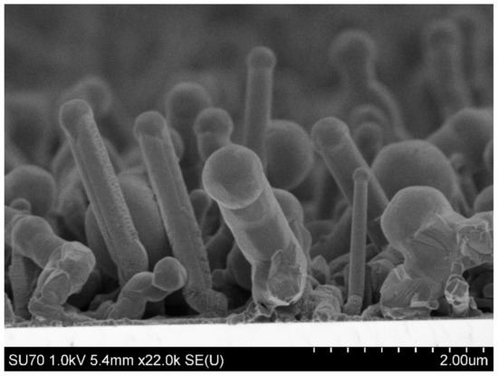
Figure 2.
SEM image showing a profile of InN nanocolumns growing upward toward the plasma source shown schematically in Figure 1. Droplets of indium metal are at the tops of nanocolumns, the indium having migrated upwards due to the electric fields present.
We have grown the GaN films reported here using a pulsed technique called Migration-Enhanced Afterglow (MEAglow). The technique is similar to atomic layer deposition (ALD) in many respects, though it operates in a higher temperature range, which is still too low to be considered metalorganic chemical vapor deposition (MOCVD). Instead of self-limiting chemistry, which characterizes ALD, MEAglow relies heavily on the deposition of a continuous metal wetting layer, which is subsequently nitrided with plasma species in order to determine the quality of the film to be deposited. Earlier results related to the technique have been described in detail elsewhere [5,11,12,13,14,15,16,17,18,19,20,21].
A brief description of the MEAglow growth system used is warranted. The most prominent feature of the system is that it has a stainless-steel hollow cathode plasma source, of the type recently used to greatly reduce oxygen contamination in ALD-grown films [22,23]. This was used to provide active nitrogen species in an ultra-high vacuum (UHV) growth chamber with load lock. There have been a number of papers [5,18,23] that have characterized this specific plasma source, which is actually the earliest prototype for some 80 other hollow cathode plasma source units that now operate around the world. However, as explained by Butcher, Georgiev and Georgieva [23], that specific design was retired from production early on in favor of designs that covered greater pressure ranges and larger deposition areas.
The plasma works as a remote radio-frequency (RF) source (13.56 MHz), with the substrates positioned in the afterglow of a nitrogen plasma. The pressure range for hollow cathodes is determined by the hole dimensions, where electrons are confined to generate the hollow cathode effect, as well as by the material of which the cathode is made (see reference [23]). Smaller holes are used for higher pressures. The design of this particular hollow cathode source is optimized for operation around 1.0 Torr with nitrogen, though the source could operate in a range from about 200 mTorr to 10 Torr. Generally, it was operated in the 1–3 Torr range for nitride film growth.
Boris et al. [24] have provided some characterization of a hollow cathode source and have pointed out that for operation below about 300 mTorr, there is a significant flux of electrons from the source, which can result in a negative floating potential for a substantial distance downstream at those pressures, and we can confirm that we have seen similar results with this source. However, in the higher pressure range used here, the floating potential at the substrate is positive, and the electrons are more closely confined to the plasma generation region. More recently, Boris et al. [25] have published a more thorough investigation of a hollow cathode plasma source. Unfortunately, for that study, they did not provide any detail of the hollow cathode itself, which makes comparison to other designs difficult; however, they have since corrected that oversight with the publication of an erratum [26]. From the 10 mm hole size mentioned in the erratum, we can confirm that the design of that cathode was optimized for operation at 300 mTorr using nitrogen. Interestingly, we note that the D.C. self-bias of the RF electrode observed during our experiments with nitrogen was below −200 V in all conditions used, which is more than an order of magnitude lower than the results reported by Boris et al. [25]. Boris et al. observed self-bias values as high as −4200 V (shown in their Figure 5) using argon/nitrogen/hydrogen mixes, which may explain the difference, since we have observed that argon mixtures tend to be harder to strike than other gases, we may investigate this at a later stage. Self-bias measurements are important, because higher values indicate the potential presence of high-energy ion species that can cause film damage.
Figure 3 shows our measurements of self-bias with nitrogen using the current plasma source covering the pressure ranges of interest for this work. These are in alignment with earlier reported measurements of the total peak-to-peak RF voltage observed for the cathode in Butcher et al. [18] Figure 4 shows the same pressure range, and the RF peak-to-peak voltages are shown not to go above 420 V. The D.C. self-bias will generally be below the applied RF peak-to-peak voltage [27], so these results are consistent with the earlier publication. It is also notable that at the highest pressure measured (6625 mTorr), the self-bias remained close to zero over the whole range of RF power. At a lower pressure of 228 mTorr, the self-bias did go up to about −610 V at 600 W of power (not shown in Figure 3); however, this system is not used in that pressure range. Even so, this value is many times lower than that which was observed by Boris et al. in the same pressure range, albeit with a different gas mixture.
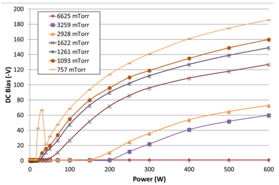
Figure 3.
Measurements of the D.C. self-bias on the RF electrode at various RF power values using a nitrogen plasma. Note that the bias values are actually in negative V.
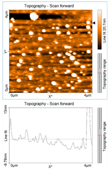
Figure 4.
AFM image of GaN sample grown under gallium-rich conditions with 45 pulse cycles (as mentioned in the text). RMS surface roughness of 9.3 nm.
The nitrogen gas pressures used here varied from about 1.2 to 1.6 Torr; at these pressures, higher energy plasma species have mainly decayed through multiple gas collisions by the time the gas reaches the substrate, so that only less-damaging species are present. Visually, the plasma is remote from the substrate. Results for hollow cathode sources that have replaced inductively coupled plasma (ICP) sources suggest that the damage from a hollow cathode source is less than an ICP source. For instance, for the ALD growth of AlN, Ozgit-Akgun [22] has observed as much as a 75% increase in the growth per cycle (GPC) when using a hollow cathode plasma source compared to previous results with an ICP source using the same growth conditions. Results from the University of Connecticut have shown an increase in film nitrogen content and, consequently, improved stoichiometry for AlN when using a hollow cathode source compared to an ICP source [28]. Because nitrogen is a volatile component of AlN, it is expected that any plasma damage would result in a lower nitrogen content in the films. It must be pointed out that some of this improvement with the hollow cathode source may also be related to the reduction in oxygen contamination, which is another advantage of using hollow cathode plasma sources [22,23].
Other evidence related to a low level of plasma damage during film growth is provided by the high quality of InN produced using this plasma source [15,19,20]. InN is particularly susceptible to plasma damage during film growth. This is shown best in Figure 2 of Butcher et al. [15], for which the presence of indium metal was identified at low-growth pressure as a result of more damaging species being able to reach the substrate during growth—causing dissociation of the InN and subsequent loss of the volatile nitrogen component. For a higher pressure, for which the plasma damage was much less, no free indium was observed. In fact, a ω-2θ X-ray diffraction full-width half-maximum value for the InN (0002) reflection of 290 arcsec was observed for growth directly on c-plane sapphire substrates, indicating a low level of defects.
Moving away from a discussion of the plasma source, the physical theory behind MEAglow-type growth [15,16,18] is similar to other forms of migration-enhanced epitaxy. At the relatively low growth temperatures used here, ~650 °C, film growth by MOCVD suffers from poor crystal quality compared to films grown at the usual MOCVD temperatures for GaN of approximately 1050 °C [1]. This drop in quality is largely related to the lower adatom mobility of gallium atoms deposited on the sample surface. At low temperatures, the gallium adatoms may have too little kinetic energy to migrate to the edge of molecular terraces. If they can migrate that far, then growth can be epitaxial and two-dimensional; if the migration is insufficient, then three-dimensional island growth occurs. As a means of overcoming this lower adatom mobility, the MEAglow technique uses pulsed metalorganic delivery. In this case, trimethylgallium (TMG) is pulsed into the system in amounts large enough to fully cover the c-plane sapphire substrates used. The growth temperatures are high enough for the decomposition of TMG, so that the gallium coverage per pulse is not limited by terminating chemistry (as occurs for ALD). In this way, the entire substrate can be covered with a wetting layer of gallium, which may be more than two monolayers thick. This also overcomes the need to have a high adatom mobility in order to achieve two-dimensional film growth. The active nitrogen is from the hollow cathode plasma source, and the nitrogen was purified down to less than parts per billion of oxygen with an in-line SAES gas purifier. The plasma source was on continuously; however, during the period in which the TMG is introduced, the active nitrogen species do not reach the substrate, as the metalorganic species quench the active nitrogen in the gas phase. No purging steps are used as in ALD. The pulse conditions used for the various experiments described in this report are provided in later sections.
Prior to loading in the film growth system, the c-plane sapphire wafers used as substrates were either degreased in solvent solutions and etched in HCl and water mixtures, or they were heated to 1050 °C in air for several hours to eliminate polishing damage visible in AFM images. A similar heat treatment methodology is reported by Cui et al. [29], though the lower anneal temperature used here was compensated for by using a much longer anneal time (>4 h). After loading, the sapphire substrates were heated to the film growth temperature under the ultimate vacuum of the system (as low as 10−8 Torr, but more typically in the low 10−7 Torr range) for an hour, before introducing a nitrogen gas flow through the plasma source at a flow rate of 1000 sccm at a chamber pressure of 750 mTorr. The RF for the plasma was then applied for 1 min at 100 W of power. This was accomplished to nitride the surface of the c-plane sapphire substrate in preparation for film growth. The advantages of sapphire nitridation for GaN film growth are well-known and described in the text by Morkoc [30].
Samples grown by the MEAGlow technique were characterized by the methods mentioned in the previous section. SIMS analysis is of particular interest. Dynamic SIMS measurements were carried out by Evan’s Analytical using a PHI quadrupole optimized for high-depth resolution and atmospheric element analysis. Metal contamination was measured with a Cameca magnetic sector using high-mass resolution and optimized for high-depth resolution. As well as the samples examined here, the Evan’s Analytical measurement configuration is suitable for very thin ALD-grown films, as demonstrated by measurements carried out for the Bilkent group [22].
XPS spectra for MEAglow-grown GaN samples were taken with a Kratos (of Manchester, UK) Axis Ultra DLD instrument. An Alkα X-ray source was used for the measurements. Mgkα X-ray sources cannot be used for this, as a gallium Auger peak interferes with the carbon signal; however, with the Alkα X-ray source, accurate gallium and nitrogen ratios are not possible, as a gallium Auger interferes with the nitrogen signal [31]. Carbon C1s surface spectra are presented here. A PANalytical X’Pert (previously of Almelo, the Netherlands) Pro MRD powder diffractometer (with a Cu anode) was used for the X-ray diffraction measurements. AFM measurements were taken with a Nanosurf (of Lietstal, Switzerland) Easyscan 2 atomic force microscope using the silicon probe model AppNano (of Mountain View, CA, USA) ACLA, with a tip radius of 6 nm. The root mean square (RMS) surface roughness values were determined from the AFM scans using the equipment vendor’s standard analysis software.
The SEM images used in this work were taken with an ultrahigh-resolution Schottky emission Hitachi (of Toronto, ON, Canada) SU 70 electron microscope. The SEM was used for cross-sectional imaging of freshly cleaved samples. A low 5 kV acceleration potential was used for the imaging, and at this low voltage, no metallization was required for charge reduction.
Optical transmission measurements were carried out either with a Cary (now of Santa Clara, CA, USA) 5e double-beam optical spectrophotometer or a Cary (now of Santa Clara, CA, USA) 50 single-beam optical spectrophotometer. An uncoated c-plane sapphire substrate was used as a reference, so that the optical absorption characteristics of the GaN films could be observed. Interference fringes from the transmission spectra were used to measure the film thicknesses. A refractive index of 2.35 was used for this, though variations due to crystal impurities can introduce large deviations from the normal refractive index. This is particularly problematic when mapping a new growth technique in which large variations in material chemistry can occur. SEM cross-sections are more accurate, though optical transmission can be used for a first-order estimate.
3. Results
Three sets of GaN film growth results are presented here. The first two sets have no grid in the system, and the film growth is shown to be gallium-rich, with excess carbon and hydrocarbons. The third set has the grid in place, and a bias of −50 V was applied. As will be shown, these latter films appear to be stoichiometric with much reduced carbon and hydrocarbon content.
3.1. Gallium-Rich Film Growth Experiments
This set of experiments was initially carried out to investigate the reason why our growth rates appeared to be significantly less than those reported by Trybus et al. [32] for a molecular beam epitaxy (MBE)-based methodology with some similarity to MEAglow. Trybus et al. had apparently succeeded in nitriding quite thick gallium layers for each growth cycle while growing p-type GaN. This particular dataset is presented here because it demonstrates some of the issues peculiar to growth with metalorganics, and also because the films were notably gallium-rich. In the end, we did have some success in growing thicker layers per cycle [5], as partially demonstrated in the next section. For this section, we are presenting an extreme situation of GaN with excess gallium and metal droplet formation, as described in greater detail elsewhere [11].
The conditions of film growth for the early experiments presented were for a metal deposition period of 30 s using a 1 sccm TMG delivery flow rate (mixed with nitrogen carrier gas downstream of the mass flow controller) and a growth temperature of 650 to 660 °C. The overall deposition period was 55 s per cycle. A flow rate of 1800 sccm of nitrogen was present through the plasma source, which was operated at 600 W. The chamber pressure was 1.6 Torr during the film growth, and substrate rotation was at 50 rotations per minute (rpm). The metalorganic delivery times are longer than are typical of ALD film growth, as the controls were based on MOCVD delivery techniques, and the amounts being delivered were much larger than for ALD, allowing for a significantly higher GPC. For comparison, in their Table 1, Ozgit-Akgun et al. [22] provide an ALD GPC value of 0.026 nm/cycle for GaN grown with a hollow cathode plasma source; the values here are over an order of magnitude higher (see, for instance, our Table 1 below). The available substrate area was approximately 4 inches in diameter, but the chamber has been made to be upgradable to a larger area, with the plasma source closer to 6 inches in diameter.

Table 1.
Table showing film thickness and absorption edge data for gallium-rich growth series.
The flow rate and pressure used here are conditions that were later found to show evidence of plasma damage for InN film growth [15]. This was shown by any extension of the nitriding time having a negative effect in terms of reducing the content of free indium metal that could still be observed in the sample by X-ray diffraction. However, at higher pressures (for the same flow rate of nitrogen from the plasma and the same delivery of trimethylindium), the indium metal signal could be reduced because of the lower amount of plasma damage incurred. The higher number of gas collisions at a higher pressure were sufficient to remove more damaging species. GaN is less susceptible to damage; however, the low melting point of gallium metal ensures that, unlike indium metal, it cannot be observed in X-ray diffraction spectra, as the gallium contribution is usually amorphous.
Figure 4 shows an AFM surface scan of one of these samples, with partially nitrided gallium metal droplets present on the sample surface after film growth. It was grown for 45 cycles using the conditions mentioned above. Many of these early film growths had gallium droplets visible on the film surfaces after growth. The optical transmission spectra for the same sample, shown in the AFM image of Figure 4, is shown in Figure 5. The transmission data for four other samples grown with the same growth conditions but with an increasing number of cycles are also shown in Figure 5.
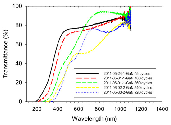
Figure 5.
Optical transmission spectra for the sample in Figure 4 grown for 45 cycles and for four other samples grown with an increasing number of cycles. All samples were etched with HCl solution to remove excess surface gallium before measurement.
What is immediately apparent from the data of Figure 5 is that, as the films grow thicker, the film absorption edge is moving to longer wavelengths. The thinnest film actually shows a 3.4 eV absorption edge, which is the band-gap expected for stoichiometric GaN. Table 1 shows the values of the absorption edge measured for each of these samples by the standard technique used to determine the band-gap for a direct band-gap semiconductor, that is, by extrapolating the linear part of the plot for an optical density squared (absorption coefficient squared can also be used) versus energy plot to the zero of the optical density squared axis. The drop in the absorption edge with material thickness is due to an increasing accumulation of impurities in the GaN. MacKenzie et al. [33] also observed a drop in the absorption edge when growing GaN at low temperatures using chemical beam epitaxy, which made use of TMG.
The second item of note from the data of Table 1 is that, even given large error bars for the values of thickness obtained from the interference fringes of Figure 5 (using a refractive index of 2.35 for stoichiometric GaN), a substantial amount of film growth has occurred in the early growth cycles compared to the later cycles. However, a significant drop in the GPC is evident even beyond 210 nm, suggesting that, in this case, substrate influences are negligible. Poisoning of the growth front is evident. Given that the films have been grown in very gallium-rich conditions, three chemical species may be suspected. These are gallium metal, perhaps in the form of surface droplets that cannot be nitrided sufficiently during the film growth, and thus block sections of the surface from further growth, or possibly in the form of free gallium incorporated in the film (see discussion in Section 4, below). Some mixture of carbon or hydrocarbons from the metalorganic and probably bound to excess gallium may also be partially or largely responsible for poisoning of the growth front, but also hydrogen itself cannot be excluded at this stage. We examine these possibilities in the following sections.
3.2. Less Gallium-Rich Film Growth Experiments
The films described in this section have been optimized to improve stoichiometry and to increase the GPC, so that thicker films could be grown without, or with less, poisoning of the growth rate. There were two contending processes involved in this. the first was to supply enough active nitrogen plasma species to improve stoichiometry for a given supply of TMG; the second issue is that the plasma itself may cause damage, so that applying the plasma for too long may actually result in nitrogen loss and a decrease in stoichiometry. An added complication was an inability to remove all the hydrocarbons associated with the TMG, so that there were still active Ga–C or Ga–CHx bonds present (this is discussed below in the Discussion section). Because of this residual contamination, the films would always remain gallium-rich compared to the nitrogen content.
The film series shown in Table 2 shows the best results we could obtain with no bias grid in the system. For this series, the TMG delivery was maintained at 0.8 sccm for 4 s, a much lower amount of TMG than for the films in the previous section, ensuring that these films were not as gallium-rich. The system pressure was maintained at 1370 mTorr (using a pressure control valve downstream of the chamber), and the plasma was on for 6.5 s per cycle. A total of 1028 cycles were used for each growth run. The growth temperature was maintained at 660 °C. To change the delivery of plasma species to the substrate, the gas flow rate from the plasma source was varied. Higher flow rates at constant pressure will deliver a greater flux of active species, but also higher energy species that could be more damaging. Other series were carried out varying the time of plasma with otherwise fixed conditions. However, this series effectively demonstrates the issues encountered. The film thicknesses for Table 2 were all obtained from SEM cross-sectional imaging of cleaved portions of the films.

Table 2.
Table showing film thickness and absorption edge data for this less gallium-rich growth series. Thickness measurements were based on SEM cross-sections.
From the table, it can be seen that a maximum GPC value of 0.257 nm/cycle was obtained at a nitrogen plasma flow rate of 1700 sccm, yielding a film thickness of 264 nm. At lower flow rates, the lower film thickness can be attributed to the delivery of insufficient amounts of active nitrogen, which left the film gallium-rich. The drop in film thickness for higher flow rates can be attributed to plasma damage, resulting in the loss of some nitrogen from the films, and again, gallium-rich films. However, the films were all found to be insulating with a yellowish tinge. When using only nitrogen as the plasma source and no bias grid, we were unable to obtain films that were conductive and clear in color, unless there was an oxygen leak in the system. Though most of the system had conflat connections, there was one O-ring related to the RF feedthrough (not used in later designs) that would occasionally fail during extended plasma operation. This would only occur once every few months. The occurrence of conductive films during an oxygen leak probably indicates that any residual carbon and hydrocarbon species bound to gallium in the films, which would normally lead to semi-insulating behavior, reacted with the oxygen to form volatile carbon monoxide and carbon dioxide species. When an oxygen leak occurred, the high level of n-type carriers introduced from oxygen in the film also overcame the insulating behavior of any remaining carbon.
It is to be noted that more aggressive plasma conditions were used for the GaN film growth than were eventually used for InN film growth. It is thought that these more aggressive conditions helped remove some of the residual carbon and hydrocarbon species. This form of contamination was not problematic for InN film growth, as the trimethylindium used decomposed quite readily at the temperatures used for that film growth.
To test the ability of the nitrogen plasma to remove carbon under more aggressive conditions, we examined two samples with XPS looking at the carbon C1s surface components. One sample was the second sample from Table 1, and the other sample was grown with a lower pressure of 1215 mTorr, which again increases the flux of higher-energy nitrogen species that reach the sample surface. An AFM image of this second sample is shown in Figure 6. Both samples were of similar thickness. The XPS results are shown in Figure 7, below.
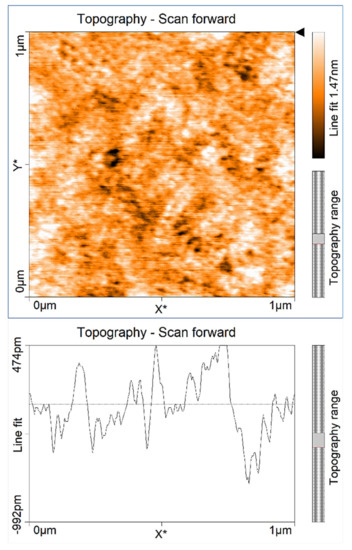
Figure 6.
AFM image of GaN sample grown under slightly gallium-rich conditions with 200 pulse cycles. RMS surface roughness of 0.24 nm.
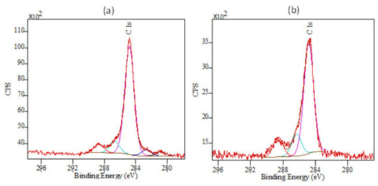
Both XPS spectra show the main 284.6 eV peak due to adventitious hydrocarbons that are immediately apparent on the surface of almost all materials after exposure to air. The higher energy peak at ~289 eV is also an adventitious peak, in this case a carbonate peak, present after exposure to air. The two lower energy peaks visible in Figure 7a between 284 and 280 eV are probably due to Ga–C and Ga–CHx bonding and are likely present due to only partially decomposed TMG. Interestingly, the same peaks are absent for the sample grown under more aggressive plasma conditions, indicating that these conditions do help remove some of the residual carbon and hydrocarbons. The small peak at approximately 286.7 eV may be due to C–N bonding and is present for both samples.
3.3. Stoichiometric GaN Film Growth
The more energetic plasma conditions presented in the previous section may have helped with the removal of some hydrocarbons and carbon from the bulk of the films, but some combination of excess gallium with carbon and hydrocarbons was still evident in the films given their yellow coloring and semi-insulating nature. The growth of thick films remained difficult. Improvement in the optical absorption edge at a given thickness of film was found to be commensurate with being able to grow thicker films, but the growth rate for the films did not remain constant, so that some level of growth-front poisoning was still evident. Figure 8 shows an image for the freshly cleaved cross-section of a GaN film on a sapphire substrate. The GaN was 500 nm thick and was grown using the same conditions as the sample with 1370 sccm in Table 2, but for 3428 cycles. The X-ray diffraction data show a single sharp peak at the (0002) reflection, shown in Figure 9. The GPC appeared to drop to an overall value of 0.15 nm/cycle for this thickness, and the absorption edge also dropped to 3.22 eV, in line with the samples still being gallium-rich.
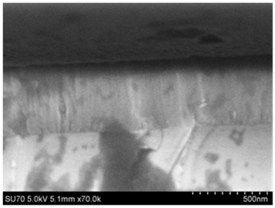
Figure 8.
SEM cross-section for a GaN film grown to 500 nm thickness on c-plane sapphire.
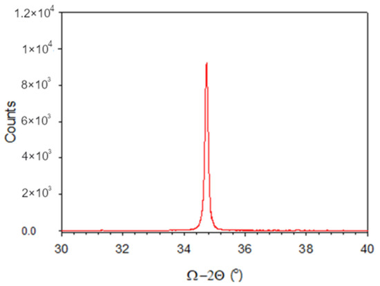
Figure 9.
X-ray diffraction data for sample of Figure 8.
Shown below in Figure 10a is an image of a film grown under similar conditions to the one above; the yellowish color of the film is strongly evident, suggesting gallium-rich film growth. In contrast, another MEAglow-grown film using the bias grid in place and biased to −50 V is shown. This second film was grown largely free of carbon contamination from the metalorganic. The carbon-free sample is clear (there is slight gallium deposition on the backside of the wafer) and conductive due to background oxygen, whereas the metal-rich sample is semi-insulating, suggesting carbon contamination. SIMS data were collected for both samples and are shown below in Figure 11 and Figure 12.
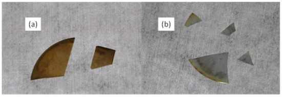
Figure 10.
Photograph of (a) sample with high carbon and (b) sample with low carbon.
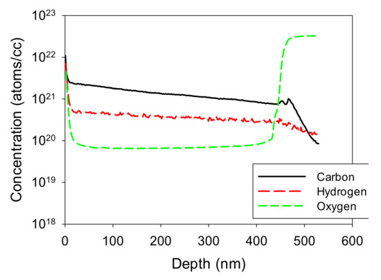
Figure 11.
SIMS data for high-carbon film shown in Figure 10a.
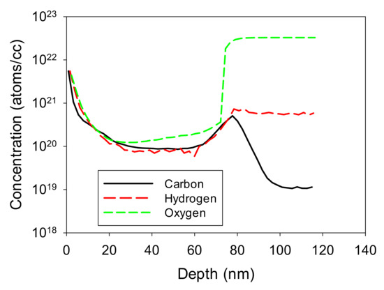
Figure 12.
SIMS data for low-carbon film shown in Figure 10b.
A series of samples were grown with the −50 V bias applied to the grid. The growth conditions used were otherwise similar to the sample grown in Figure 10a: the nitrogen gas flow was 1700 sccm, the chamber pressure was 1370 mTorr, the plasma-only time was for a slightly longer period of 8 s. In this case, the TMG was delivered for 4 s, but the TMG flow rate was varied to determine the best growth conditions for the fixed nitrogen plasma conditions. The substrate rpm was dropped to 10, but this was because no difference was seen compared to the higher rotation rate used for the earlier films. Only 1500 cycles were used. The results are shown in Table 3 below.

Table 3.
Table showing film thickness and absorption edge data for samples grown with −50 V bias in place. The film thicknesses data were based on UV-Vis transmission data and are only approximate.
From Table 3 and the absorption edge data, an optimum value (the film thicknesses measurements are affected by the noise associated with using the UV-Vis transmission data) appears to occur at around 0.44 or 0.45 sccm of TMG. This is substantially less than that which was required for the data of Table 2, for which 0.8 sccm was used. Similar optimum values of absorption are observed for both Table 2 and Table 3; however, as expected, for the high carbon sample of Figure 10a, SIMS shows carbon to be the dominant contaminant in the film, with levels increasing from 1021 cm−3 near the sapphire substrate (at ~450 nm) to higher levels nearer the sample surface. Hydrogen is less plentiful than carbon, but still much higher than oxygen, at about 3 × 1020 cm−3, but also increasing towards the sample surface. It seems that contamination from hydrocarbons was growing worse as the film growth progressed. The level of oxygen in the film may also seem high compared to commercial MOCVD-grown GaN, with a bulk film value of about 7 × 1019 cm−3. However, this film has been grown directly on sapphire with no buffer layer, and it is consequently polycrystalline with a strong wurtzite columnar growth habit. It is known that oxygen diffusion down grain boundaries after exposure to air can occur for epitaxial polycrystalline material [34]. Accordingly, this 0.4% level of oxygen content would indicate grains that are 860 nm in diameter, as found using the calculation procedures provided by Butcher et al. [34].
For the low-carbon film of Figure 10b, the SIMS results are shown in Figure 12. For this figure, the carbon and hydrogen are at much lower levels than for the sample of Figure 11, and they are at approximately the same levels as the oxygen signal, indicating that these are probably all adventitious species that have migrated down grain boundaries in the material and are present there as monolayers. Oxygen is at approximately 1 × 1020 cm−3, which indicates grain boundaries of approximately 600 nm in diameter. These can be compared to the 190 nm-diameter grain boundaries achieved by Burnham et al. [35] using metal modulated epitaxy (MME), which is an MBE technique with some similarity to MEAglow.
Finally, in Figure 13, we show a comparison of the absorption edges of the two samples from Figure 10. Instead of an optical density square plot, in this case, the y-axis is the absorption coefficient squared, so that the absorption data are independent of film thickness. In the plot, the high-carbon sample shows significant band tailing at lower energies, indicating a large density of defects, whereas the low-carbon sample has a relatively sharp absorption edge, indicating better-quality material.
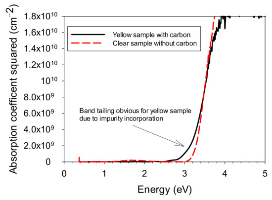
Figure 13.
Absorption coefficient squared data for the two samples of Figure 10.
4. Discussion
From our experiments, we observed problems with high carbon and hydrocarbon contamination, but also gallium-rich material, which occurred in part because of this contamination. For the relatively low growth temperatures used for these experiments, as compared to MOCVD (~650 °C compared to >950 °C), carbon and hydrocarbon retention from the TMG used as the gallium metal source becomes problematic. More generally, the use of low-temperature thin film growth techniques with metalorganics—for example, plasma-enhanced atomic layer deposition (PEALD), but also plasma-enhanced chemical vapor deposition (PECVD) techniques—is complicated by the susceptibility to contamination by high levels of carbon and hydrocarbons from precursor materials.
Examples of high carbon contamination in ALD- and PEALD-grown films are common for many material systems. For instance, in 2013, Eddy et al. [36] mentioned carbon contamination during the atomic layer epitaxy of group III nitrides as a primary source of point defects, requiring further process development to combat. Carbon contamination in TiN grown with metalorganics has been shown to increase sheet resistivity, an unwanted effect for that material [37,38]. Even work with a material as robust as silicon nitride can be adversely affected by carbon contamination when using metalorganics at low growth temperatures [39]. Nitrides are not the only materials that can be affected by carbon contamination; copper deposited by ALD using metalorganics has also been shown to have high carbon/hydrocarbon contamination [40]. Meanwhile, Lee and Kang [41] found the resistivity of aluminum metal deposited by ALD was relatively high due in part to the 3% residual carbon left by the metalorganic used. In a 2019 paper, Jin et al. [42] studied carbon-related contamination in ALD-grown Al2O3 layers when using different oxygen sources. In a recent review paper, Leskela, Mattinen and Ritala [43] note that a high carbon background is a general problem for III-V compounds deposited by atomic layer epitaxy (ALE) from metalorganics. Knoops et al. [44] mention high carbon levels in a number of materials when using plasma-based ALD techniques and metalorganics.
Likewise, there are examples of high carbon and hydrocarbon contamination for other low-temperature methods of film growth, including PECVD, in which the substrate is in the plasma itself, and also remote PECVD (RPECVD), in which the plasma source is upstream of the growth region, so that more damaging ions and electrons are considered “remote” from the substrate, as per the growth system schematic of Figure 1 above. For instance, Butcher et al. [45,46] observed high hydrocarbon and hydrogen levels in AlN grown near room temperature by RPECVD, but they were able to reduce these by photolytic desorption methods. Interestingly, they were also able to improve film adhesion to mercury cadmium telluride substrates by the removal of surface hydrocarbons using similar methods [47]. Meikle et al. [48] showed that at higher growth temperatures of 300 °C and 500 °C, RPECVD of AlN resulted in a large amount of carbon when using just a nitrogen gas plasma and trimethylaluminium. Sone et al. [49] observed very high SIMS levels of carbon (1020 to 1021 cm−3) in GaN grown by RPECVD at 800 °C, and though the use of hydrogen as a gettering agent reduced this to a certain extent, high levels of 1019 cm−3 were still evident.
For this paper, we concentrated on the particular problem of carbon contamination from trimethylgallium for the low-temperature deposition of gallium nitride. The work of Danielsson et al. [50] indicates that high carbon incorporation from trimethylgallium in GaN may be problematic for temperatures below about 900 °C, and they measured carbon SIMS levels of 1.2 × 1020 cm−3 for material grown by MOCVD at 800 °C. At higher growth temperatures, precursor decomposition is more readily completed, and chemical gettering or scavenging processes with hydrogen, ammonia and other reducing agents can also help with the removal of volatile carbon-containing byproducts. However, at lower temperatures, these processes are much less effective. The growth temperature may be such that precursor decomposition is incomplete, and/or scavenging processes may also be ineffective or have unwanted consequences, such as hydrogen retention.
A number of techniques have been actively applied at lower temperatures to reduce carbon and hydrocarbon contamination. A quick list of these is provided here:
- (1)
- New precursors have been developed with lower decomposition temperatures and/or with no direct hydrocarbon bonds to the metal cation species [51].
- (2)
- Prolonged plasma exposure can be used to reduce the concentration of hydrocarbons and carbon species. This can be effective to a point, though plasma etching of the main material being deposited may also result if plasma exposure occurs for too long. Often, multiple processes are present in a plasma, involving UV light emission, ions and various radical reactions, so these processes can be quite complicated. Because of the complexity of these processes, results are best obtained by empirical experimentation, though the complete removal of carbon-based species is rarely obtained by these means alone; more often, plasma exposure with a reactive species is more effective (method 5, below). For plasma by itself, the work of Knoops et al. [39] is indicative of the effectiveness of this process. For silicon nitride, they saw a reduction in carbon from about 20% to about 7% when increasing plasma exposure time from 1 to 15 s (see their Figure 4).
- (3)
- In a variation of method 2, Shih et al. [52] used an argon ion bombardment to remove hydrogen and hydrocarbons during the PEALD of AlN, resulting in the growth of high-quality epitaxial material.
- (4)
- Photodesorption using filtered ultraviolet light has been shown to be successful for the production of high-resistivity AlN (3.3 × 10¹⁶ Ω·cm) grown at near-room temperature by RPECVD [45,46].
- (5)
- Hydrogen or ammonia, and in some cases, oxygen-bearing species, are sometimes used to reduce metalorganics used during deposition. For instance, Deminskyi et al. [53] recently reported the use of an ammonia plasma to decrease the carbon content for InN grown by ALD. However, at very low temperatures, hydrogen retention can be problematic when using hydrogen or ammonia. Butcher et al. [45] found that AlN and Al grown by laser induced CVD and RPECVD at near-room temperature retained so much hydrogen when using hydrogen or ammonia gas that the films were pyrophoric when exposed to air. Semiconductor doping can also become difficult if too much hydrogen is present in the lattice. P-type doping of GaN with Mg often requires a rapid thermal anneal step to remove hydrogen and activate the dopants [54]; however, this can only be achieved if the hydrogen content of the films is low to begin with.
The technique used here may have some advantages over the ones listed above, which each have their strengths and weaknesses. For instance, we are only using a nitrogen plasma, so that hydrogen retention in the films is low. There is no extra process time due to added process steps, and the ease of implementation is high. At the moment, the main drawback is a lack of understanding of the mechanism.
In regard to the excess gallium that was evident for some of the films grown here, there have been past reports of quite large inclusions of gallium metal in GaN grown at low temperatures, though the mode of incorporation for the excess gallium is still only partially understood. Blant et al. [55] have speculated as to the location of excess gallium in GaN grown by plasma-assisted molecular beam epitaxy (PAMBE) on sapphire at 750 °C, and they suggested that excess gallium may be present at grain boundaries. The importance of excess gallium for thin ~20 nm-thick GaN nucleation layers (then called buffer layers) grown by PAMBE is also discussed by Kim et al. [56,57], who identified large amounts of excess gallium in their material grown directly on sapphire, without identifying a location for the percentage amounts of excess gallium shown to be present in their nucleation films.
However, there are significant differences between PAMBE growth at relatively low GaN growth temperatures and CVD-based growth at similar temperatures. In particular, a considerable amount of residual carbon and possibly hydrocarbons from the metalorganic can still be present in the case of CVD-based growth. This is because although two of the methyl groups from TMG can readily be desorbed as methane and ethane dissociation byproducts, the third methyl group is very resilient and may only give up some of its hydrogen during related byproduct reactions [58,59,60]. In short, for the low-temperature growth of GaN using TMG, there is a propensity to have some small amount of residual carbon and perhaps, to a lesser extent, hydrogen present [58].
Samples grown under these conditions, with excess carbon present, are usually found to be semi-insulating, and indeed, the gallium-rich samples described above were all semi-insulating. Undoped GaN grown by MOCVD at high temperatures normally has a low-level n-type background due to unintentional oxygen contamination (oxygen substituting nitrogen acts as an n-type dopant [61,62]). However, intentional carbon doping is used to create semi-insulating GaN [50,62], so it is believed here that residual carbon from the metalorganic was responsible for the semi-insulating nature of the GaN samples, though native defects related to the gallium-rich stoichiometry cannot be ruled out.
Biasing the grid placed between the plasma source and the substrate to −50 V allowed films to be grown that were relatively free of carbon and hydrocarbon contamination. The mechanism by which this occurred is unclear. It might be speculated that the negative bias was repelling residual ions from the plasma source, which were damaging the same sample. However, such ions would have been gettered when grounding the same grid above the sample, and yet the same effect was not seen. Further, to remove the residual carbon and hydrocarbons, a driving force or energy is needed, such as ion bombardment. Therefore, if the ions are repelled by the grid, what is the mechanism that removes these contaminating species? We know from our previous work that there can be electromigration of metal species on the surface of the substrate when an electric field is applied [5] by the plasma or otherwise. A positive bias above the substrate strongly attracts liquid metal droplets formed from the top metal wetting layer. It is probable that a form of electromigration is also occurring when the grid is biased to −50 V; the negative voltage would repel liquid metal, causing some turbulence at the surface of the liquid melt of the wetting layer, and this might cause other non-metal compounds, such as hydrocarbons and carbon-bound species, to be driven to the surface of the wetting layer, where they can be more effectively removed. However, this is only speculation. The effect requires further investigation. Unfortunately, biasing the grid to −100 V caused a local plasma between the grid and the sample holder, so it was not possible to go to higher negative bias in this growth system.
Having a means of obtaining low carbon/hydrocarbon contamination in films, especially when using a nitrogen-only plasma, has some advantage over using ammonia or hydrogen as carbon-gettering agents. Although there is some indication of excess hydrogen in the SIMS of the high-carbon film (Figure 11), in this case, we see higher levels of carbon, so that the excess hydrogen is most likely associated with partially decomposed hydrocarbons, and it is likely to be present as C–H groups. The hydrogen in the low-carbon film of Figure 12 is due to ex situ exposure to air, which has ingressed along the crystal boundaries of the c-plane-oriented film. It would be useful to grow the GaN on an MOCVD template epitaxially to see how low the carbon and hydrogen contents were in the bulk crystal without this ex situ component (this is possible at these temperatures).
In contrast to our films, we note that the SIMS measurements of GaN, which was grown using ALD with an ammonia plasma and presented by Ozgit-Akgun et al. [22] in their Figure 1b, indicates high hydrogen in their films at levels that are more than two orders of magnitude higher than the carbon in these films. The high hydrogen content in that case would be from the hydrogen in the plasma species used. The large amount of excess hydrogen in their films may also be taking up gallium and/or nitrogen bond sites that would normally be accommodated by GaN-related bonds.
5. Conclusions
We have examined the growth of GaN from trimethylgallium (TMG) and nitrogen plasmas activated with a hollow cathode plasma source at low temperatures around 650 °C. We confirmed that, as expected from other methods of film growth at such a low temperature, significant carbon/hydrocarbon contamination occurs from the TMG, resulting in semi-insulating films with a yellowish appearance. However, a novel method of carbon and hydrocarbon removal was found; the use of a negatively biased grid between the plasma source and the substrate allowed the GaN to be grown with no detectable carbon or hydrocarbon contamination above that seen from ex situ exposure to the ambient atmosphere. The results were confirmed using SIMS, optical measurements and visual observations. The grid was not used for ion or electron flux control, since the substrate was remote from the plasma. However, the negative electric field of the grid would cause the repulsion of liquid gallium metal in the deposited wetting layer on top of the GaN. Such electromigration effects have been utilized with the liquid phase epitaxy technique termed electroepitaxy. We speculate that this repulsion caused turbulence in the wetting layer that helped move residual carbon and hydrocarbon species to the surface of the melt, where they could more easily be removed as volatile species.
Author Contributions
Conceptualization, K.S.A.B.; methodology, K.S.A.B., R.G., P.T. and P.W.B.; validation, K.S.A.B., V.G., D.G., R.G., P.T. and P.W.B.; formal analysis, K.S.A.B., V.G., D.G., R.G., P.T. and P.W.B.; investigation, K.S.A.B., V.G., D.G., R.G., P.T. and P.W.B.; data curation, K.S.A.B.; writing—original draft preparation, K.S.A.B.; writing—review and editing, K.S.A.B., V.G., D.G., R.G., P.T. and P.W.B.; visualization, K.S.A.B.; supervision, K.S.A.B.; project administration, K.S.A.B.; funding acquisition, K.S.A.B. All authors have read and agreed to the published version of the manuscript.
Funding
This work was funded by the National Research Council of Canada through its Industrial Research Assistance Program (IRAP) (project number: 732744).
Institutional Review Board Statement
Not applicable.
Informed Consent Statement
Not applicable.
Data Availability Statement
The authors confirm that the data supporting the findings of this study are available within the article.
Acknowledgments
Our thanks to Gary Mount, previously of Evans Analytical, for their aid in carrying out the SIMS measurements.
Conflicts of Interest
The authors declare no conflict of interest. The funders had no role in the design of the study; in the collection, analyses or interpretation of data; in the writing of the manuscript or in the decision to publish the results.
References
- Pearton, S.J.; Zolper, J.C.; Shul, R.J.; Ren, F. GaN: Processing, defects, and devices. J. Appl. Phys. 1999, 86, 1–78. [Google Scholar] [CrossRef]
- Butcher, K.S.A.; Afifuddin; Chen, P.P.-T.; Godlewski, M.; Szcerbakow, A.; Goldys, E.M.; Tansley, T.L.; Freitas, J.A., Jr. Recrystallization prospects for freestanding low-temperature GaN grown using ZnO buffer layers. J. Crystal Growth 2002, 246, 237–243. [Google Scholar] [CrossRef]
- Lawrence, D.J.; Eastman, L.F. Electric current controlled liquid phase epitaxy of GaAs on N+ and semi-insulating substrates. J. Electron. Mat. 1977, 6, 1–24. [Google Scholar] [CrossRef]
- Jastrzebski, L.; Lagowski, J.; Gatos, H.C.; Witt, A.F. Liquid-phase electroepitaxy: Growth kinetics. J. Appl. Phys. 1978, 49, 5909–5919. [Google Scholar] [CrossRef]
- Butcher, K.S.A.; Terziyska, P.T.; Gergova, R.; Georgiev, V.; Georgieva, D.; Binsted, P.W.; Skerget, S. DC voltage fields generated by RF plasmas and their influence on film growth morphology through static attraction to metal wetting layers: Beyond ion bombardment effects. J. Appl. Phys. 2017, 121, 013301. [Google Scholar] [CrossRef]
- Li, S.Q.; Liang, Y.X.; Guo, T.L.; Lin, Z.X.; Wang, T.H. Synthesis of vertically electric-field-aligned In2O3 nanowires. Mater. Lett. 2006, 60, 1492–1495. [Google Scholar] [CrossRef]
- Nozaki, T.; Okazaki, K. Carbon Nanotube Synthesis in Atmospheric Pressure Glow Discharge: A Review. Plasma Process. Polym. 2008, 5, 300–321. [Google Scholar] [CrossRef]
- Bower, C.; Zhu, W.; Jin, S.; Zhou, O. Plasma-induced alignment of carbon nanotubes. Appl. Phys. Lett. 2000, 77, 830–832. [Google Scholar] [CrossRef]
- Gosh, S.; Polaki, S.R.; Kamruddin, M.; Jeong, S.M.; Ostrikov, K. Plasma-electric field controlled growth of oriented graphene for energy storage applications. J. Phys. D Appl. Phys. 2018, 51, 145303. [Google Scholar] [CrossRef]
- Qi, Y.; Deng, B.; Guo, X.; Chen, S.; Gao, J.; Li, T.; Dou, Z.; Ci, H.; Sun, J.; Chen, Z.; et al. Switching Vertical to Horizontal Graphene Growth Using Faraday Cage-Assisted PECVD Approach for High-Performance Transparent Heating Device. Adv. Mater. 2018, 30, 1704839. [Google Scholar] [CrossRef]
- Terziyska, P.T.; Butcher, K.S.A.; Alexandrov, D. Investigation of the presence of metal droplets after pulsed InN and GaN epitaxial growth using atomic force microscopy and nanoindentation. Appl. Surf. Sci. 2012, 258, 9997–10001. [Google Scholar] [CrossRef]
- Terziyska, P.T.; Butcher, K.S.A.; Gogova, D.; Alexandrov, D.; Binsted, P.; Wu, G. InN nanopillars grown from In-rich conditions by migration enhanced afterglow technique. Mater. Lett. 2013, 106, 155–157. [Google Scholar] [CrossRef]
- Terziyska, P.T.; Butcher, K.S.A.; Rafailov, P.; Alexandrov, D. Growth of vertically oriented InN nanorods from In-rich conditions on unintentionally patterned sapphire substrates. Appl. Surf. Sci. 2015, 353, 103–105. [Google Scholar] [CrossRef]
- Terziyska, P.T.; Butcher, K.S.A. Self-Catalytic Growth of InN Nanowires. Bulg. J. Phys. 2016, 43, 54–63. Available online: http://www.bjp-bg.com/paper1.php?id=801 (accessed on 6 October 2022).
- Butcher, K.S.A.; Alexandrov, D.; Terziyska, P.; Georgiev, V.; Georgieva, D.; Binsted, P.W. InN grown by migration enhanced afterglow (MEAglow). Phys. Status Solidi A 2012, 209, 41–44. [Google Scholar] [CrossRef]
- Butcher, K.S.A.; Alexandrov, D.; Terziyska, P.; Georgiev, V.; Georgieva, D. Initial Experiments in the Migration Enhanced Afterglow Growth of Gallium and Indium Nitride. Phys. Status Solidi C 2012, 9, 1070–1073. [Google Scholar] [CrossRef]
- Binsted, P.W.; Butcher, K.S.A.; Alexandrov, D.; Terziyska, P.; Georgieva, D.; Gergova, R.; Georgiev, V. InN on GaN Heterostructure Growth by Migration Enhanced Epitaxial Afterglow (MEAglow). Mat. Res. Soc. Sym. Proc. 2012, 1396, 255–260. [Google Scholar] [CrossRef]
- Butcher, K.S.A.; Kemp, B.W.; Hristov, I.B.; Terziyska, P.; Binsted, P.W.; Alexandrov, D. Gallium Nitride Film Growth Using a Plasma Based Migration Enhanced Afterglow Chemical Vapor Deposition System. Jpn. J. Appl. Phys. 2012, 51, 01AF02. [Google Scholar] [CrossRef]
- Tran, N.H.; Le, B.H.; Fan, S.; Zhao, S.; Mi, Z.; Schmidt, B.A.; Savard, M.; Gervais, G.; Butcher, K.S.A. Optical and structural characterization of nitrogen-rich InN: Transition from nearly intrinsic to strongly n-type degenerate with temperature. Appl. Phys. Lett. 2013, 103, 262101. [Google Scholar] [CrossRef]
- Gergova, R.; Butcher, K.S.A.; Binstead, P.W.; Gogova, D. Initial results for epitaxial growth of InN on gallium oxide and improved Migration-Enhanced Afterglow Epitaxy growth on gallium nitride. J. Vac. Sci. Technol. B 2014, 32, 031207. [Google Scholar] [CrossRef]
- Togtema, G.; Georgiev, V.; Georgieva, D.; Gergova, R.; Butcher, K.S.A.; Alexandrov, D. GaN–InGaN LED efficiency reduction from parasitic electron currents in p-GaN. Solidi State Electron. 2015, 103, 44–48. [Google Scholar] [CrossRef]
- Ozgit-Akgun, C.; Goldenberg, E.; Okyay, A.K.; Biyikli, N. Hollow cathode plasma-assisted atomic layer deposition of crystalline AlN, GaN and AlxGa1−xN thin films at low temperatures. J. Mater. Chem. 2014, 2, 2123–2136. [Google Scholar] [CrossRef]
- Butcher, K.S.A.; Georgiev, V.; Georgieva, D. Recent Advances in Hollow Cathode Technology for Plasma-Enhanced ALD—Plasma Surface Modifications for Aluminum and Stainless-Steel Cathodes. Coatings 2021, 11, 1506. [Google Scholar] [CrossRef]
- Boris, D.R.; Wheeler, V.D.; Nepal, N.; Qadri, S.B.; Walton, S.G.; Eddy, C.R. The role of plasma in plasma-enhanced atomic layer deposition of crystalline films. J. Vac. Sci. Technol. A 2020, 38, 040801. [Google Scholar] [CrossRef]
- Boris, D.R.; Johnson, M.J.; Eddy, C.R.; Walton, S.G. Hollow cathode enhanced capacitively coupled plasmas in Ar/N2/H2 mixtures and implications for plasma enhanced ALD. J. Vac. Sci. Technol. B 2022, 40, 044002. [Google Scholar] [CrossRef]
- Boris, D.R.; Johnson, M.J.; Eddy, C.R.; Walton, S.G. Erratum: ‘‘Hollow cathode enhanced capacitively coupled plasmas in Ar/N2/H2 mixtures and implications for plasma enhanced ALD” [J. Vac. Sci. Technol. B 40, 044002 (2022)]. J. Vac. Sci. Technol. B 2022, 40, 057001. [Google Scholar] [CrossRef]
- Kim, J.-H.; Shin, Y.-H.; Chung, K.-H. Study on self-bias voltage induced on the substrate by r.f. bias power in a high-density plasma. Thin Solid Films 2003, 435, 288–292. [Google Scholar] [CrossRef]
- Mohammad, A.; Shukla, D.; Ilhom, S.; Willis, B.; Johs, B.; Kemal Okyay, A.; Biyikli, N. Real-time in situ ellipsometric monitoring of aluminum nitride film growth via hollow-cathode plasma-assisted atomic layer deposition. J. Vac. Sci. Technol. A 2019, 37, 020927. [Google Scholar] [CrossRef]
- Cui, J.; Sun, A.; Reshichkov, M.; Yun, F.; Baski, A.; Morkoç, H. Preparation of Sapphire for High Quality III-Nitride Growth. MRS Internet. J. Nitride Semicond. Res. 2000, 5, e7. [Google Scholar] [CrossRef]
- Morkoc, H. Handbook of Nitride Semiconductors and Devices, Volume 1: Materials Properties, Physics and Growth; Wiley-VCH Verlag Gmbh & Co.: Weinheim, Germany, 2008; pp. 346–350. [Google Scholar]
- Zatsepin, D.A.; Boukhvalov, D.W.; Buntov, E.A.; Zatsepin, A.F.; Batalov, R.I.; Novikov, H.A.; Bayazitov, R.M. Effect of pulsed ion-beam treatment on the electronic and optical properties of GaN epitaxial films on sapphire. Appl. Surf. Sci. 2020, 590, 153023. [Google Scholar] [CrossRef]
- Trybus, E.; Doolittle, W.A.; Moseley, M.; Henderson, W.; Billingsely, D.; Namkoong, G.; Look, D.C. Extremely high hole concentrations in c-plane GaN. Phys. Status Solidi C 2009, 6, S788–S791. [Google Scholar] [CrossRef]
- MacKenzie, J.D.; Abemathy, C.R.; Stewart, J.D.; Muhr, G.T. Growth of Group III nitrides by chemical beam epitaxy. J. Cryst. Growth 1996, 164, 143–148. [Google Scholar] [CrossRef]
- Butcher, K.S.A.; Timmers, H.; Afifuddin Chen, P.P.-T.; Weijers, T.D.M.; Goldys, E.M.; Tansley, T.L.; Elliman, R.G.; Freitas, J.A., Jr. Crystal size and oxygen segregation for polycrystalline GaN. J. Appl. Phys. 2002, 92, 3397–3403. [Google Scholar] [CrossRef]
- Burnham, S.D.; Henderson, W.; Doolittle, W.A. Closed-loop MBE growth of droplet-free GaN with very metal rich conditions using Metal Modulated Epitaxy with Mg and In. Phys. Status Solidi C 2008, 5, 1855–1858. [Google Scholar] [CrossRef]
- Eddy, C.R., Jr.; Neepal, N.; Hite, J.K.; Maestro, M.A. Perspectives on future directions in III-N semiconductor research. J. Vac. Sci. Technol. A 2013, 31, 058501. [Google Scholar] [CrossRef]
- Musschoot, J.; Xie, Q.; Deduytsche, D.; Van den Berghe, S.; Van Meirhaeghe, R.L.; Detavernier, C. Atomic layer deposition of titanium nitride from TDMAT precursor. Microelectron. Eng. 2009, 86, 72–77. [Google Scholar] [CrossRef]
- Burke, M.; Blake, A.; Povey, I.M.; Schmidt, M.; Petkov, N.; Carolan, P.; Quinn, A.J. Low sheet resistance titanium nitride films by low-temperature plasma-enhanced atomic layer deposition using design of experiments methodology. J. Vac. Sci. Technol. A 2014, 32, 031506. [Google Scholar] [CrossRef]
- Knoops, H.C.M.; Braeken, E.M.J.; de Peuter, K.; Potts, S.E.; Haukka, S.; Pore, V.; Kessels, W.M.M. Atomic Layer Deposition of Silicon Nitride from Bis(tert-butylamino)silane and N2 Plasma. ACS Appl. Mater. Interfaces 2015, 7, 19857–19862. [Google Scholar] [CrossRef]
- Gordon, P.G.; Kurek, A.; Barry, S.T. Trends in Copper Precursor Development for CVD and ALD Applications. ECS J. Solidi State Sci. Technol. 2015, 4, N3188–N3917. Available online: https://iopscience.iop.org/article/10.1149/2.0261501jss (accessed on 6 October 2022). [CrossRef]
- Lee, Y.J.; Kang, S.-W. Atomic Layer Deposition of Aluminum Thin Films Using an Alternating Supply of Trimethylaluminum and a Hydrogen Plasma. Electrochem. Sol. State Lett. 2002, 5, C91–C93. Available online: https://iopscience.iop.org/article/10.1149/1.1503204 (accessed on 6 October 2022). [CrossRef]
- Jin, H.S.; Kim, D.H.; Kim, S.K.; Wallace, R.M.; Kim, J.; Park, T.J. Strategic Selection of the Oxygen Source for Low Temperature-Atomic Layer Deposition of Al2O3 Thin Film. Adv. Electron. Mater. 2019, 5, 1800680. [Google Scholar] [CrossRef]
- Leskela, M.; Mattinen, M.; Ritala, M. Review Article: Atomic layer deposition of optoelectronic materials. J. Vac. Sci. Technol. B 2019, 37, 030801. [Google Scholar] [CrossRef]
- Knoops, H.C.M.; Faraz, T.; Arts, K.; Kessels, W.M.M. Status and prospects of plasma-assisted atomic layer deposition. J. Vac. Sci. Technol. A 2019, 37, 030902. [Google Scholar] [CrossRef]
- Butcher, K.S.A.; Tansley, T.L.; Li, X.; Zhou, B. Photolytic Absorbate Removal During the Growth of Aluminum Nitride by Remote Microwave Plasma Chemical Vapour Deposition. Sol. State Electron. 1997, 41, 305–314. [Google Scholar] [CrossRef]
- Butcher, K.S.A.; Tansley, T.L. Ultrahigh resistivity aluminum nitride grown on mercury cadmium telluride. J. Appl. Phys. 2001, 90, 6217. [Google Scholar] [CrossRef]
- Butcher, K.S.A.; Tansley, T.L.; Prince, K.; Leech, P.W. Predeposition ultraviolet treatment for adhesion improvement of thin films on mercury cadmium telluride. J. Vac. Sci. Technol. A 2001, 19, 90–96. [Google Scholar] [CrossRef]
- Meikle, S.; Nomura, H.; Nakanishi, Y.; Hatanaka, Y. Reactions of atomic nitrogen and trimethyl aluminum downstream from a nitrogen microwave plasma. J. Appl. Phys. 1990, 67, 483–486. [Google Scholar] [CrossRef]
- Sone, S.; Kim, M.H.; Kim, H.J.; Yoon, E. Effects of hydrogen on carbon incorporation in GaN grown by remote plasma-enhanced metal-organic chemical vapor deposition. J. Crystal Growth 1998, 189–190, 321–324. [Google Scholar] [CrossRef]
- Danielsson, O.; Li, X.; Ojamae, L.; Janzen, E.; Pedersen, H.; Forsberg, U. A model for carbon incorporation from trimethyl gallium in chemical vapor deposition of gallium nitride. J. Mater. Chem. C 2016, 4, 863–871. [Google Scholar] [CrossRef]
- Rouf, P.; Samii, R.; Rönnby, K.; Bakhit, B.; Buttera, S.C.; Martinovic, I.; Ojamäe, L.; Hsu, C.-W.; Palisaitis, J.; Kessler, V.; et al. Hexacoordinated Gallium(III) Triazenide Precursor for Epitaxial Gallium Nitride by Atomic Layer Deposition. Chem. Mater. 2021, 33, 3266–3275. [Google Scholar] [CrossRef]
- Shih, H.-Y.; Lee, W.-H.; Kao, W.-C.; Chuang, Y.-C.; Lin, R.-M.; Lin, H.-C.; Shiojiri, M.; Chen, M.-J. Low-temperature atomic layer epitaxy of AlN ultrathin films by layer-by-layer, in-situ atomic layer annealing. Sci. Rep. 2017, 7, 39717. [Google Scholar] [CrossRef] [PubMed]
- Deminskyi, P.; Rouf, P.; Ivanov, I.G.; Pedersen, H. Atomic layer deposition of InN using trimethylindium and ammonia plasma. J. Vac. Sci. Technol. A 2019, 37, 020926. [Google Scholar] [CrossRef]
- Gotz, W.; Johnson, N.M.; Walker, J.; Bour, D.P.; Street, R.A. Activation of acceptors in Mg-doped GaN grown by metalorganic chemical vapor deposition. Appl. Phys. Lett. 1996, 68, 667–669. [Google Scholar] [CrossRef]
- Blant, A.V.; Novikov, S.V.; Cheng, T.S.; Flannery, L.B.; Harrison, I.; Campion, R.P.; Korakakis, D.; Larkins, E.C.; Kribes, Y.; Foxon, C.T. Ga-metal inclusions in GaN grown on sapphire. J. Crystal Growth 1999, 203, 349–354. [Google Scholar] [CrossRef]
- Kim, Y.; Shapiro, N.A.; Feick, H.; Armitage, R.; Weber, E.R.; Yang, Y.; Cerrina, F. Elastic strain relief in nitridated Ga metal buffer layers for epitaxial GaN growth. Appl. Phys. Lett. 2001, 78, 895–897. [Google Scholar] [CrossRef]
- Kim, Y.; Subramanya, S.G.; Siegle, H.; Kruger, J.; Perlin, P.; Weber, E.R.; Ruvimov, S.; Liliental-Weber, Z. GaN thin films by growth on Ga-rich GaN buffer layers. J. Appl. Phys. 2000, 88, 6032–6036. [Google Scholar] [CrossRef]
- Lam, H.-T.; Vohs, J.M. Surface reactions of trimethylgallium on MOVPE-grown GaN(0001). Surf. Sci. 1999, 426, 199–211. [Google Scholar] [CrossRef]
- Aquino, A.A.; Hill, J.J.; Jones, T.S. Evidence for a surface methylene species in the decomposition of trimethylgallium on GaAs(100)-(4 × 1): A high resolution electron energy loss spectroscopy study. Surf. Sci. 1995, 327, 74–80. [Google Scholar] [CrossRef]
- Bahlawane, N.; Reilmann, F.; Salameh, L.-C.; Kohse-Höinghaus, K. Mass-spectrometric monitoring of the thermally induced decomposition of trimethylgallium, tris(tert-butyl)gallium, and triethylantimony at low pressure conditions. J. Am. Soc. Mass. Spectrum 2008, 19, 947–954. [Google Scholar] [CrossRef][Green Version]
- Van de Walle, C.G.; Neugebauer, J. First-principles calculations for defects and impurities: Applications to III-nitrides. J. Appl. Phys. 2004, 95, 3851–3879. [Google Scholar] [CrossRef]
- Tang, H.; Fang, Z.Q.; Rolfe, S.; Bardwell, J.A.; Raymond, S. Growth kinetics and electronic properties of unintentionally doped semi-insulating GaN on SiC and high-resistivity GaN on sapphire grown by ammonia molecular-beam epitaxy. J. Appl. Phys. 2010, 107, 103701. [Google Scholar] [CrossRef]
Publisher’s Note: MDPI stays neutral with regard to jurisdictional claims in published maps and institutional affiliations. |
© 2022 by the authors. Licensee MDPI, Basel, Switzerland. This article is an open access article distributed under the terms and conditions of the Creative Commons Attribution (CC BY) license (https://creativecommons.org/licenses/by/4.0/).