Review

Electron-Beam Synthesis of Dielectric Coatings Using Forevacuum Plasma Electron Sources (Review)

1
Department of Physics, Tomsk State University of Control Systems and Radioelectronics, 634050 Tomsk, Russia
2
High Current Electronics Institute Russian Academy of Sciences, 634055 Tomsk, Russia
*
Author to whom correspondence should be addressed.
Coatings 2022, 12(1), 82; https://doi.org/10.3390/coatings12010082
Submission received: 3 December 2021 / Revised: 2 January 2022 / Accepted: 4 January 2022 / Published: 12 January 2022
(This article belongs to the Special Issue Electron-Ion-Plasma Technology Applied to Surface Engineering)

Abstract

:
This is a review of current developments in the field of ion-plasma and beam methods of synthesis of protective and functional dielectric coatings. We give rationales for attractiveness and prospects of creating such coatings by electron-beam heating and following evaporation of dielectric targets. Forevacuum plasma electron sources, operating at elevated pressure values from units to hundreds of pascals, make it possible to exert the direct action of an electron beam on low-conductive materials. Electron-beam evaporation of aluminum oxide, boron, and silicon carbide targets is used to exemplify the particular features of electron-beam synthesis of such coatings and their parameters and characteristics.

1. Introduction

Dielectric coatings based on oxides, nitrides, borides, carbides, and other compounds take up a special place among various functional and protective thin-film coatings. Such coatings are normally characterized by high hardness, temperature, and corrosion resistance, with the majority of them being electrically insulating [1]. Ceramic coatings, deposited onto the metal surfaces, are used to protect them from thermal and mechanical damage, corrosion, and premature wear. Such coatings are widely used in the automotive and aerospace industries, nuclear energy, and medicine. For the first time, ceramic coatings have begun to be used in the aerospace industry for covering the gas turbine engine blades exposed to increased corrosive and erosive wear due to constant temperature changes. In the nuclear energy industry, they are used to cover the elements of the reactors, cooling systems, and nuclear fuel storages. In the military-industrial complex, ceramic compounds are used to cover equipment cases, weapon elements, and special products. The coatings used in metalworking increase the hardness and lifetime of the parts. In the automotive industry, ceramic materials are used to protect components of engines, rims, and chassis; in medicine, they are used to protect devices and parts of prostheses. Thin boron-containing films (pure boron, boron carbide, or nitride) are widely used in microelectronics, nuclear power, and aerospace due to their high hardness, strength, wear resistance, chemical inertness, and dielectric properties, as well as the ability of boron to absorb neutron radiation.
For many industrial applications, it is desirable for the coatings to combine these properties at a relatively low production cost. For example, aluminum oxide, the most commonly used dielectric in virtually all industries, is a chemically inert, corrosion-resistant material with a relatively low cost as compared with other ceramics. Its hardness (15–20 GPa) is on par with hard alloys and its specific resistance (1014 Ω·cm) with the best electrical insulating materials [2]. Coatings based on aluminum oxide can operate at temperatures up to 1500 °C and find wide applications in modern instrument and mechanical engineering [3]. Boron-based coatings, boron nitride and metal borides, are of considerable interest. These compounds are chemically inert, temperature resistant, and have high hardness. The hardness of cubic boron nitride surpasses that of diamond, and its decomposition temperature is twice as high as that of diamond [4]. Note that boron-containing surface layers are created today most often by using the filler brazing technology [5] or the more up-to-date technology of gas borating in the atmosphere of decomposing, usually toxic, gaseous boron compounds [6].
The search results for the keywords “dielectric coatings” in publications of the American Institute of Physics (AIP), Institute of Electrical and Electronic Engineers (IEEE), Institute of Physics (IOP), Elsevier, American Institute of Aeronautics and Astronautics (AIAA), and other institutions show a significant increase in the number of articles on this topic over the last five years (Figure 1).
Beam-plasma methods of creating multifunctional dielectric coatings in vacuum or a rarefied gas, such as magnetron spattering, vacuum arc plasma deposition, laser ablation, electron-beam evaporation, and plasma-enhanced chemical methods, are used for addressing a wide range of practical problems related to surface modification of various materials. Among the extensive nomenclature of beam-plasma technologies, the electron-beam synthesis of coatings is characterized by a faster deposition rate and, hence, higher productivity [7]. Creation of dielectric coatings by electron-beam evaporation is hampered due to the electrical charging of the evaporated surface of the target. To neutralize the charging, it is necessary, at least at the initial stage of the technological process, to employ special methods and approaches [8] that complicate the equipment and diminish control over the process and its efficacy.
Forevacuum plasma electron sources are capable of generating electron beams in the previously inaccessible forevacuum range of elevated pressure (1–100 Pa). They have the same usual advantages of conventional plasma electron sources: high current density, reliability, they are non-sensitive to rough vacuum conditions and the presence of active gases. The plasma formed in the electron-beam transport region at an elevated pressure of the forevacuum range effectively neutralizes the surface charging of non-conductive materials by the electron beam [9]. This opens up a principal opportunity for using forevacuum plasma electron sources for electron-beam evaporation of dielectric materials and creating coatings [10]. Additionally, the beam plasma, generated in the forevacuum pressure range, can be used to provide ion-plasma assistance for electron-beam synthesis of dielectric coatings or modification of the surface properties of dielectric materials [11,12].
This article is a review of the current research on the creation of dielectric coatings by forevacuum plasma electron sources in comparison with the known methods of the beam and ion-plasma synthesis of such coatings.

2. Beam and Ion-Plasma Methods of Dielectric Coating Deposition

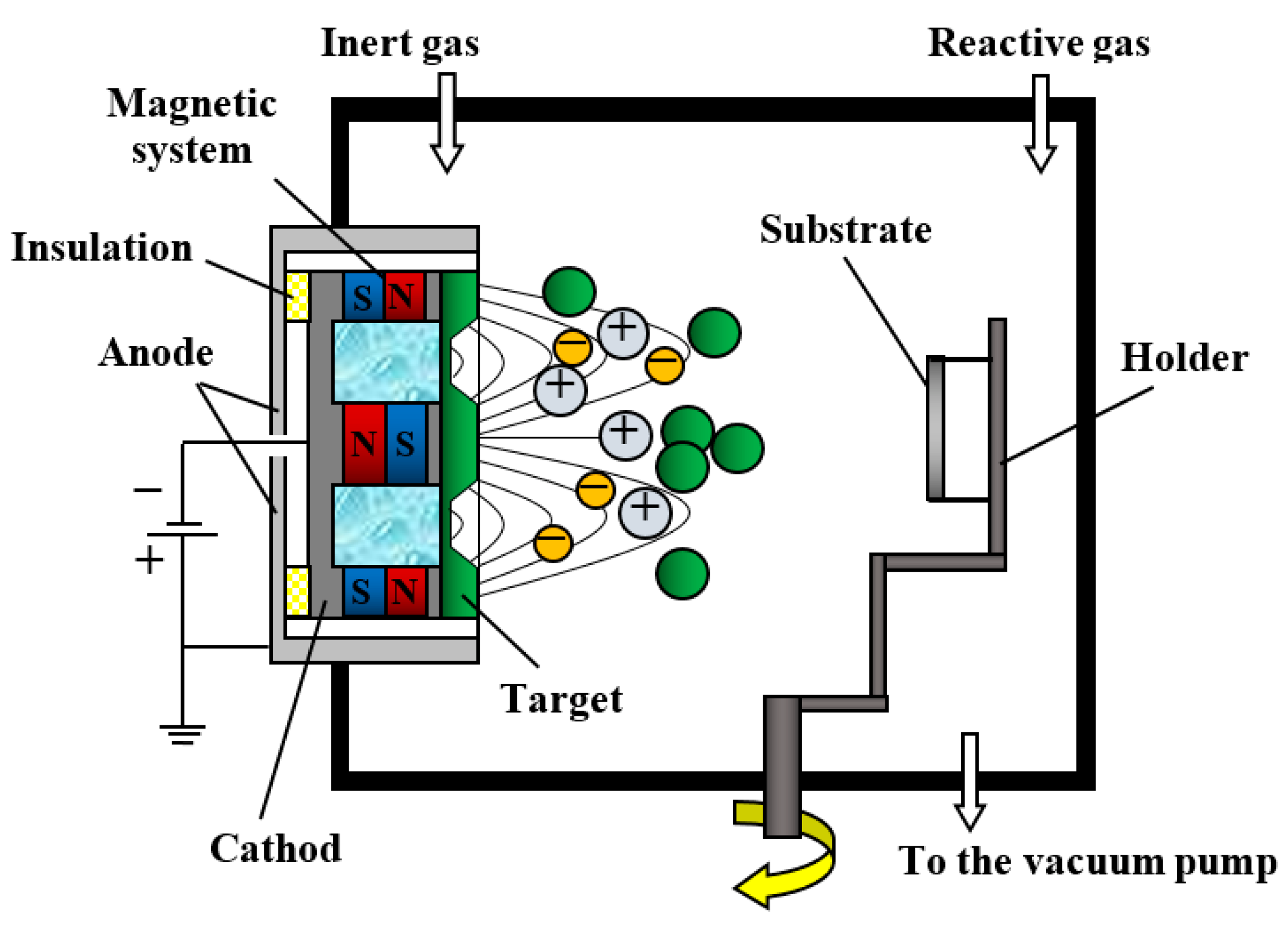
2.1. Magnetron Sputtering

Magnetron sputtering is one of the most common methods of coating deposition [13]. In its essence, it is the sputtering of a cathode target by ions from the plasma generated in a magnetron discharge system, which is a type of discharge in crossed electric (E) and magnetic (H) E × H fields. A magnetron discharge normally occurs in the planar geometry of electrodes with a magnetic field of an arc configuration. Such sputtering systems operate at a working gas pressure of 10−2 to 1 Pa and provide a deposition rate of various metal coatings at about 15 nm/min. Physical processes in magnetron sputtering systems (MSS) related to metal coating deposition on various surfaces have been a subject of thorough studies and have been discussed in much detail; see, for example [14].
The MSS-based methods of dielectric coating fabrication can be conventionally divided into three groups: reactive magnetron sputtering that uses chemically active gases; high-frequency magnetron sputtering of a dielectric target; dielectric target heating to ensure sufficient electrical conductivity. Under magnetron sputtering, the deposition rate of dielectric coatings is much lower than that of metal films.
A schematic diagram of a system with reactive magnetron sputtering is shown in Figure 2 [15].
In this system, a chemically active gas (oxygen, nitrogen, etc.), being added to the inert gas in the vacuum chamber, chemically reacts with the sputtered material of the target and forms a dielectric film on the substrate. In this way, one can deposit coatings of complex composition based on oxides, nitrides, carbides, and other materials [16,17]. Along with a number of advantageous features associated with the widespread use of reactive magnetron sputtering, the technique carries certain fundamental disadvantages. They include the “disappearance” of the anode when a dielectric film is formed on its surface [18], as well as the “contamination” of the MSS target [19] and intense arcing on its surface [20]. The indicated problems can be partially resolved by replacing the standard MSS system with a dual system that implements more stable sputtering [21], but, all in all, such systems degrade the stability of the coating deposition and have a negative effect on the quality of coatings.
A dielectric target can be sputtered in a radio-frequency (RF) magnetron discharge, which is essentially an electrodeless discharge. An RF magnetron can sputter dielectrics whose composition is close to that of the coating [22]. The most often used frequency is 13.56 MHz [23]. Such systems are used to deposit ferroelectric layers to form capacitor structures in micro- and nanoelectronics [24] and protective and reflective layers in optical storage devices [25]. They also find their applications in the deposition of wear- and corrosion-resistant coatings such as SiO2, Al2O3, and other chemical compounds [26]. However, because of the complexity of matching the output parameters of the RF generator with the parameters of the discharge gap, the RF magnetron sputtering is practically not used for coating large-area substrates. Besides, the RF power supply is more costly and the coating deposition rate is relatively slow, not exceeding several tens of nanometers per minute [27].
In the case of using a target of boron or other low-conductive materials under normal conditions, but with sufficient conductivity for the discharge to operate at high temperatures, heating the target is deemed an expected and apparent approach to the problem. Such an approach is implemented, for example, in a magnetron system with a cathode target of pure boron [28] (a material with resistivity under normal conditions of about 107 Ω·cm). In [29] (Figure 3), the boron target was heated up to a temperature of 600–700 °C in 1–2 min by an auxiliary steady low-current glow discharge, which can initiate even on a cold boron target. At such temperatures, the electrical conductivity of the target rises to a value sufficient for the burning of a pulsed magnetron discharge, with current amplitude of 20–50 A and pulse duration of up to 150 µs. At such a high discharge current, the so-called self-sputtering regime is realized in MSS [30], in which the fraction of boron ions in the discharge plasma can exceed 90%. In this way, it is possible to produce boron-based coatings, but the main problem posed here is cracking and destruction of the pure boron target due to the mechanical stress caused by heating.
Let us consider the possibility of the self-sputtering regime in the pulsed magnetron discharge system with a pure boron cathode described in papers [31,32]. The use of a bipolar voltage pulse, in combination with negative potential applied to the collector, ensured stable burning of the magnetron discharge with a frequency of 300–350 kHz, which is much lower than the «standard» magnetron frequency (13.5 MHz). This method was used in those papers to obtain boron-based coatings in various gases. The study of their composition and morphology showed that the smoothest coating was deposited in the case of boron sputtered in a residual atmosphere or in pure nitrogen, while the presence of oxygen greatly increased the surface roughness. Studies of the coating morphology showed that the best uniform and defect-free coatings are the boron-based ones obtained in a nitrogen or residual atmosphere, while with the boron-oxygen plasma, the deposited coatings have a coarse-grained structure.

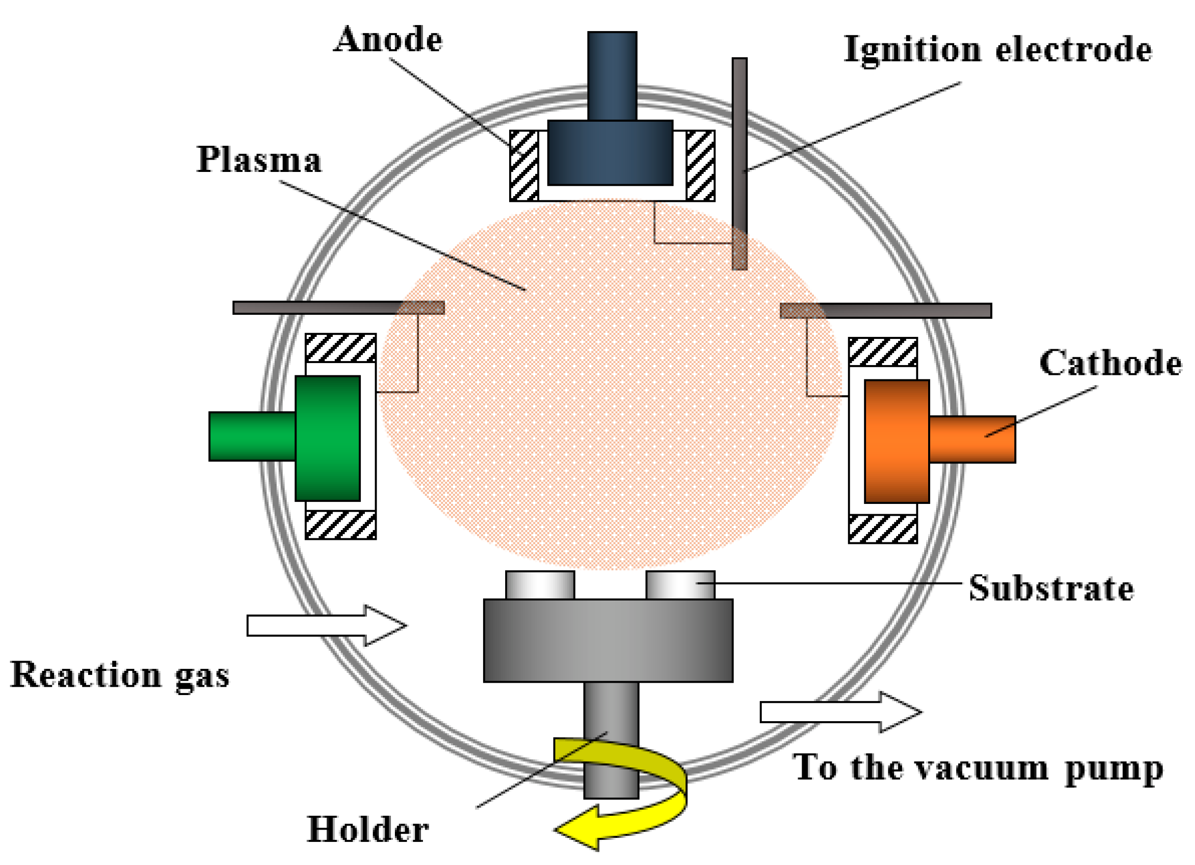
2.2. Cathodic Arc System

Vacuum arc, or cathodic arc deposition of coatings, is a method of creating coatings in vacuum by condensing a material onto the substrate from plasma fluxes generated in the cathode spot of a vacuum (cathode) arc, which is a high-current low-voltage discharge operating exclusively in metal vapor of the cathode material [33]. The definite advantages of the vacuum arc method are high deposition rates, amounting to several tens of nanometers per minute [34], and good adhesion of coating to the substrate [35]. It is owing to these properties that electric arc evaporators have found their industrial applications [36]. An inherent disadvantage of arc evaporators is the presence of micro-droplet fractions, whose deposition significantly diminishes the coating properties [37]. The use of various filtering systems, predominantly magnetic filters with a 90-degree rotation of the plasma flux [38], significantly decreases the surface contamination by vapor of the cathode material. Besides making the design of arc evaporators more complex, filtration of the plasma flux degrades the deposition rate to the level of magnetron sputtering [39].
As in magnetron sputtering systems, to produce coatings with dielectric and semiconductor properties, a reaction gas (nitrogen, methane, or oxygen) is fed into the working chamber [40]. An example of such a process that uses an arc evaporator is illustrated in Figure 4 [41].
This method is used to produce TiN, AlTiN, TixOy, AlTiSiN, TiCN, CrxNy, and other coatings [42]. As a rule, the first stage of deposition includes ion cleaning of the surface, which is performed by applying to it a voltage of several kilovolts supplied by a high-voltage source. After the voltage is brought down to the level of 100 V, the sputtered particles begin to condense onto the substrate in an atmosphere of a particular reaction gas. As an example, one may consider the use of a cathode arc for deposition of heat- and erosion-resistant coatings on the turbine blades of aircraft engines. The base of such coatings is a strong nickel alloy (85–75% Ni; 10–15% Al; 5–10% Cr), with aluminum oxide Al2O3 forming on its surface, whose protective properties are preserved up to a temperature of 1500 °C [43]. This method is used to produce TiO2 films, with a dielectric constant of 25–38 and a dielectric loss tangent of 0.01–0.02, which can be used as optical coatings and dielectrics of capacitor structures for integrated microcircuits with multilevel wiring [44]. The deposition rate of dielectric coatings in arc systems with an admission of reaction gases is about 17 nm/min [45], which is much higher than in HF magnetron sputtering systems [46] or in magnetrons with an admission of reaction gases [47]. Despite the presence of a micro-droplet fraction, the use of a vacuum arc seems quite beneficial for these purposes.
As in magnetron sputtering systems, it is possible to produce dielectric coatings in arc systems by initiating a cathode spot on a preliminary heated solid cathode, which under normal conditions is a dielectric or a semiconductor with low electrical conductivity. Consider as an example the discharge system of an ion source based on a vacuum arc discharge with a crystalline boron cathode [48]. A schematic diagram of the installation is shown in Figure 5 [49].
A vacuum arc discharge between the cathode made of pure crystalline boron and the hollow anode operates at a residual pressure of 10−6 torr. As a result of high-voltage breakdown between the cathode and the tungsten ignition electrode occurring along the surface of the ceramic insert, cathode spots of the vacuum arc are initiated. To heat the cathode to a temperature of about 600 °C, in order to ensure sufficient electrical conductivity upon the discharge ignition, a coil heater, made of 0.7 mm tungsten wire, is used around the molybdenum cathode holder. As noted in [50], upon ignition of the arc with a pure boron cathode, due to a considerable difference in electrical conductivity, the cathode spots in the initiation and adjacent areas almost stay still, or move slowly over the cathode surface. This brings about local erosion of the cathode and a large amount, as compared with a metal cathode, of micro-droplets [50].
A somewhat smaller micro-droplet fraction in the boron arc plasma has been achieved by the multi-point initiation of an arc discharge using a tungsten grid instead of a dielectric insert, and by igniting the spots at the grid contacts with the cathode surface [51].

2.3. Plasma-Enhanced Chemical Methods
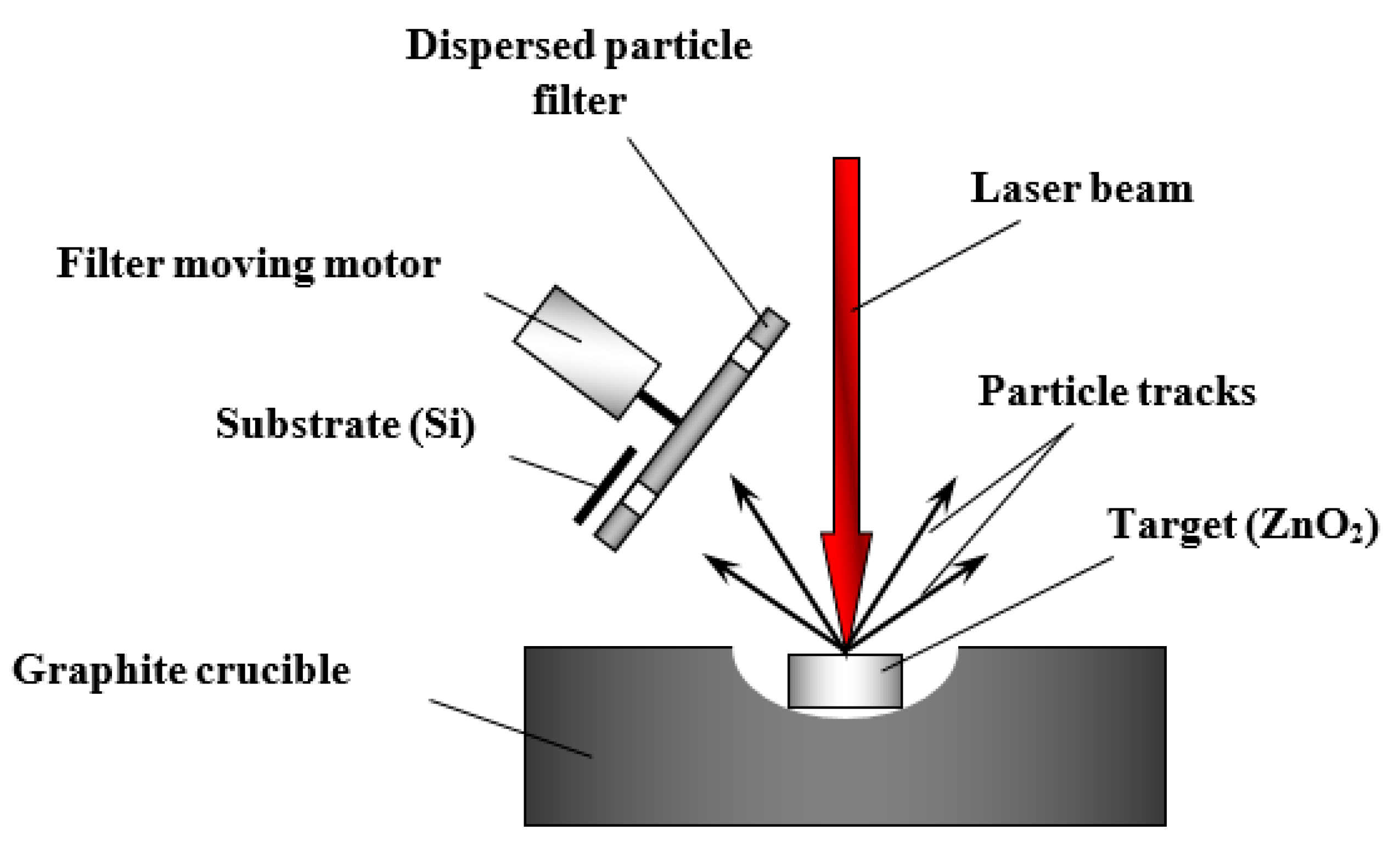
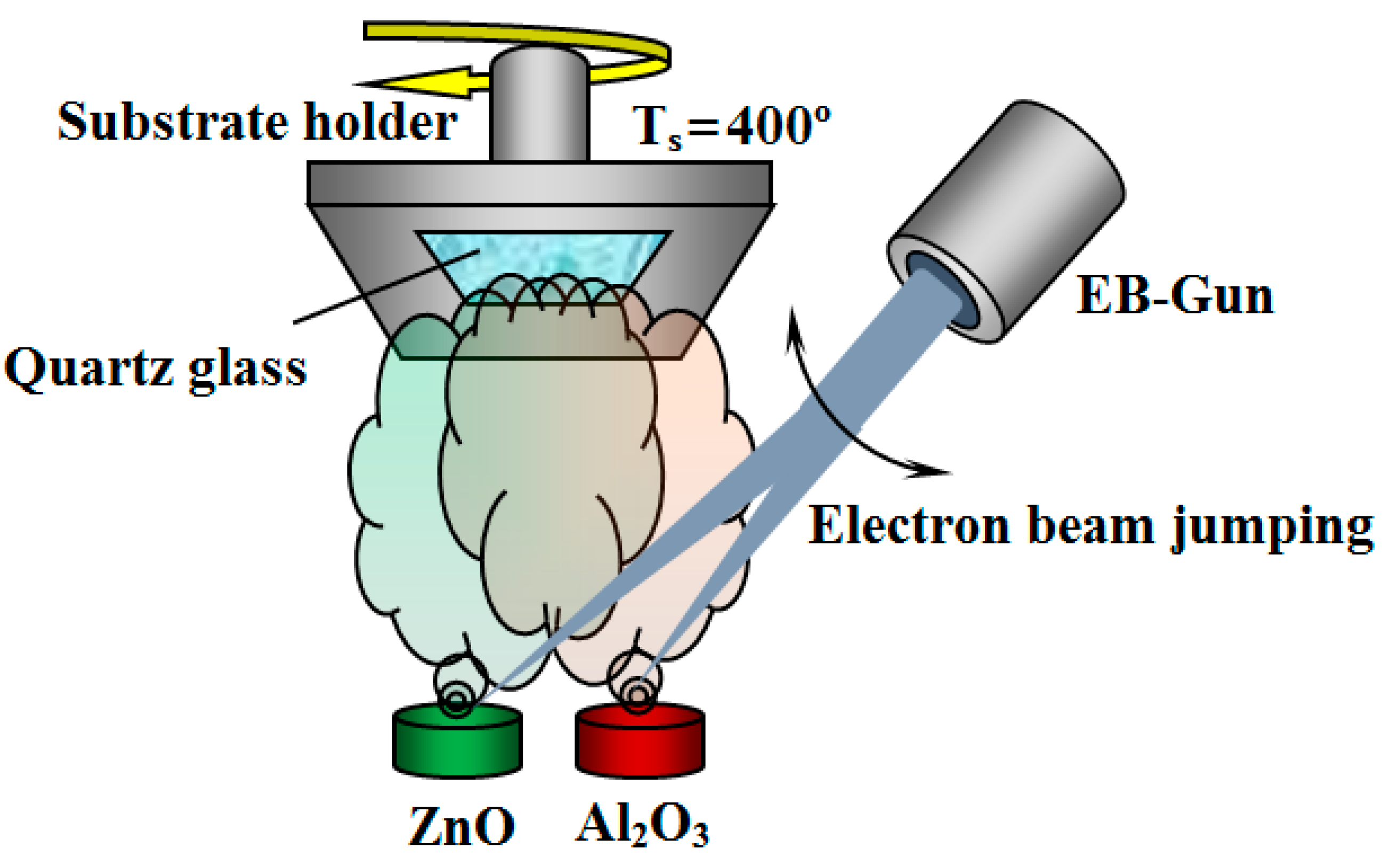
Plasma-enhanced chemical vapor deposition (PECVD) is a deposition method in which a coating is formed as a result of a chemical reaction occurring in plasma [52]. Under such a method, auxiliary plasma is used to decompose the reacting substances and activate the substrate surface. The plasma-enhanced chemical method is distinguished from other methods by its relatively low process temperature, which is less than 400 °C. This feature extends the range of materials suitable for coating deposition, including polymers [53].
For any plasma-enhanced chemical deposition method, it is first necessary to determine the optimal plasma parameters that ensure maximum efficiency. The existing methods of plasma generation for PECVD can be conventionally subdivided into two groups: discharge and beam ones. The first group includes the techniques where plasma is generated in low-pressure discharges, such as a glow discharge [54], vacuum arc [55], HF- [56], or UHF- [57] discharge. The beam group includes the use of electron beams [58], laser radiation [59], and, in a number of cases, ion beams [60].
The creation of plasma by an electron beam has certain fundamental advantages, of which the most important is the high efficiency of energy transfer when acting on the gas reaction volume. There are practically no limitations for an electron beam on the chemical composition of the medium into which it is injected [61]. It can be generated in cavities, which allows the internal surfaces of the parts to be coated [62] and solid bodies to be introduced into the reaction volume [63]. An electron beam can be injected not only into a gas, but also into a gas flow [64]; it is also possible to combine it with other plasma-generating sources [65].
The PECVD method is employed to create thick diamond-like films [66], as well as ceramics based on silicon nitride and oxide [67], aluminum oxide [68], and nitride [69]. A schematic diagram of plasma-enhanced chemical vapor deposition using an electron beam for the synthesis of silicon dioxide is shown in Figure 6 [70]. In this reactor, an electron beam, generated by an electron gun with an accelerating voltage of 30 kV and a beam current of 2 mA, is formed in a 20 L vacuum chamber.
An electron beam is focused in the gas-dynamic output window with a diameter of 2 mm, through which it is injected into the reactor working chamber with a volume of 150 L. The components of the plasma-forming medium, Si (C2H5O)4 + O2, are fed into the same chamber. The electron beam, interacting with the plasma-forming medium in the chamber, forms a cloud of electron-beam plasma, into which a sample is introduced. As a result of the interaction between the electron beam and the active medium, gas molecules effectively dissociate when they collide with electrons. The reaction products deposit on the substrate and form a coating. The growth rate of dielectric coatings in such reactors in the process of complex chemical reactions can reach hundreds of nanometers per minute [71]. Table 1 contains typical parameters of dielectric coatings deposited by the PECVD method.
Figure 7 [72] shows pictures of the cross-section of the α-Al2O3 coating on the surface of tool steel produced by an electron-beam plasma reactor, whose working principle is similar to the installation in Figure 6. It is possible in principle to produce dielectric coatings with a thickness of a few microns using the plasma-enhanced chemical method. However, along with a tight packing of particles, the coatings also contain pores with a diameter of tens of nanometers, as well as larger pores with a diameter of up to 2 µm. Hence, for a wider application of the PECVD method in depositing coatings with high uniformity of properties, the method should be further developed.
Another drawback of this method is the difficulty in controlling the gas and vapor composition as they decompose, which leads to the presence of a broader range of gas products in coatings [53]. Besides, it is difficult to control the coating thickness and uniformity [73]. An industry-level plasma-chemical reactor is a complex and cumbersome installation that incorporates expensive power supply and vacuum evacuation systems [74]. Plasma-chemical reactors with an electron beam often make use of hot cathode guns. Since the pressure range that provides a stable operation of hot cathode electron sources is 2–3 orders of magnitude lower than the optimal pressure required for plasma-chemical reactions, a design of complex and costly differential pumping systems is needed.
The electron-beam plasma-chemical reactor can be significantly simplified if one makes use of special electron sources, which produce accelerated electrons within the range of reactor optimal working pressure. Forevacuum plasma electron sources meet these requirements. The work in this direction is being carried out at the US Naval Research Laboratory (NRL). They created a Large Area Plasma Processing System (LAPPS) [75], which is based on the selection and acceleration of electrons from the discharge plasma with an extended hollow cathode and the formation of a flat surface “plasma sheet” in the electron-beam transport region. A schematic diagram of LAPPS installation is shown in Figure 8 [76]. “Plasma sheet” ions make it possible to process extended flat parts, including etching, coating synthesis, nitriding, etc.
At a pressure of 2–13 Pa, the LAPPS installation can generate a ribbon electron beam, 1 cm thick and 30 cm long, with a current density of up to 10 mA/cm2 and electron energy of up to 2 keV. The density of plasma generated by the electron beam is n = 109–1012 cm−3 at the electron temperature Te = 0.5 eV. The installation has narrow ranges of working pressure and electron-beam parameters, which considerably reduces the efficiency of the LAPPS-type systems. The efficiency is lower mainly due to the low pressure values: The electron beam goes through the gas utilizing only a small fraction of its energy. Despite this, the advantage of LAPPS is in its ability to provide high uniformity of the plasma and high quality of the coating.

2.4. Laser Methods

Laser coating deposition consists in ablation of a target material by laser radiation, followed by the deposition of vapor on the surface [77]. Presently, laser technologies are used to produce coatings of various materials [78] in a wide range of pressure, up to atmospheric. Of the coatings fabricated by laser ablation, one may mention layers of high-temperature superconductors [79], semiconductor structures [80], oxide- or other ceramic-based dielectric coatings [81], as well as diamond-like coatings [82]. By changing the wavelength of laser radiation, power, energy density, and the pulse duration, one can control the coating thickness and uniformity [83].
Laser synthesis of dielectric coatings can be conventionally divided into three groups: ablation of metals in a medium of chemically active gases [84]; blazing or cladding of dielectric materials (nanopowders) onto a substrate [85]; direct evaporation of a dielectric target [86]. The first method is in principle similar to the ion-plasma methods of a vacuum arc coating deposition. In this case, the laser beam is used either to vaporize metal in an active gas (oxygen, nitrogen) and deposit non-conductive coatings, such as titanium oxide, or to excite plasma in plasma-chemical reactors. The laser cladding is the most widely used technique. This method is used to obtain coatings of up to several millimeters thick.
A schematic diagram demonstrating the basic principle behind the synthesis of coatings by laser evaporation of a target is shown in Figure 9 [87]. The coatings are deposited in a pulsed laser evaporation mode at a wavelength λ = 1.06 µm or in a continuous mode at λ = 10.6 µm. The most important parameter that governs the physics and chemistry of laser deposition is the mode in which the laser operates. It determines the temperature in the evaporation zone, rate of evaporation, the mechanism of nucleation, and structure and properties of coatings. When using a continuous or pulsed laser, the interaction of the material vapor with radiation and the target becomes essential.
Most energy of laser radiation is spent on heating the vapor and much less on its creation. For this reason, the target evaporation rate, at all other conditions being equal, is significantly lower for continuous radiation than for the case of a nanosecond pulsed radiation, when the vapor screening the target surface does not have enough time to form. Effective evaporation of semiconductors and dielectrics occurs at the following parameters of laser radiation: wavelength 1 µm, frequency 10 kHz, pulse duration 200 ns, power density per pulse 107–108 W/cm2.
A high-power laser is usually placed outside the vacuum chamber. An optical system guides the laser beam into the chamber through an optically transparent window and focuses it on the target. The characteristic penetration depth of laser radiation into the target surface is only 10 nm. Only a thin surface layer of the material is exposed to radiation (the skin depth is typically 15–20 nm), while the temperature of the rest of the target remains virtually unchanged. This is the main specific feature of the target ablation by powerful pulsed laser systems.
Depending on the intensity and localization of laser radiation, the products of ablation can be either atoms, ions, molecules or particulate clusters and micro-particles that move with high kinetic energy from the area of the laser action to the surface. When interacting with the target surface, radiation may create droplet fractions, but this problem is solved by using filters, similar to those used in vacuum arc devices [88].
Paper [89] presents the results of fabricating zirconium dioxide coatings deposited on silicon substrates. The experimental setup is shown in Figure 10 [89].
The experiments used a solid-state pulsed Nd: YAG laser based on SKAT-301 laser facility with an active medium of YAG (Y3Al5O12) doped with neodymium ions Nd [90]. The laser operated in the single-pulse mode with laser radiation intensity of 108–1010 W/m2, and in the pulse-frequency mode at a pulse repetition rate of 50–100 Hz. The target was made of remelted chemically pure dielectric powder of ZrO2. The silicon sample was located at 10 mm from the evaporated target. A rotating filter was used to filter out the deposition of particles with a diameter 0.1–1 µm on the substrate. Coating layers with a thickness of up to 500 nm were obtained in this manner. The study of adhesion properties of coatings showed that zirconium dioxide particles detached from each other at a load of 100 mN, while the detachment of the coatings from the substrate occurred at a relatively low value of 10 mN.
In papers [91,92], boron nitride coatings were deposited by laser ablation of a target made of pure (99.99%) boron nitride. They used a Lambda Physik LPX300 excimer laser [93] with a wavelength of 248 nm, pulse duration of 30 ns, and energy per pulse of 0.9 J. The coatings were deposited in the vacuum chamber at a residual gas pressure of 10−7 Pa. The size of the laser spot was 2 mm × 3 mm, and the coating thickness was controlled by the pulse counts. The target was placed at an angle of 45 degrees to the substrate surface, which rotated to ensure a uniform coating. Boron nitride coatings were obtained on silicon, alumina ceramics, and silicon dioxide, including hexagonal and cubic phases.
The essential specifics of all devices used for depositing coatings on the target surface by the laser ablation method is the necessity for an input window to let laser radiation into the vacuum chamber, where the actual deposition of coating on the substrate surface occurs. Like the substrate surface, the inner window surface is also subject to the deposition of vaporized material, whose film obstructs penetration of radiation through the window. To diminish this effect, a reflecting system of mirrors is installed in the chamber, which allows placing the window in the area with a minimal flux of ablated material. This prolongs the window’s period of use without cleaning, but does not solve the problem of its dusting.
Laser ablation is specific in that the laser power density in the focused laser spot is high, up to a hundred watts per square centimeter. This feature allows the laser to be successfully used in various technological processes, such as cutting of materials or surface hardening, but it does not give any benefits in coating deposition. The heating of the target at a power density exceeding a threshold value causes its explosive boiling and contaminates the flux of evaporated material with a droplet fraction.
So, evaporation of the target material by laser ablation for coating deposition is a fairly efficient technique. However, the need to place the evaporated target in vacuum does not grant laser ablation any apparent advantages as compared with the electron-beam method of coating deposition. It should be noted that the development of laser ablation techniques greatly benefits from the availability of high-power lasers; though expensive, they are reliable, with a long history of development, and are produced commercially on a mass scale for various tasks at hand.

2.5. Electron-Beam Methods

Electron-beam method of coating deposition consists in melting and evaporation of a solid-body target by an electron beam, followed by the deposition of the evaporated material on a substrate [94]. Electron-beam coating deposition has the following characteristic advantages:
-
High electron-beam energy density, up to 10 MW/cm2, at which the temperature attainable in the beam action area is sufficient to melt virtually any material;
-
Capability to effectively control the parameters of the electron beam and its position;
-
Possibility of obtaining chemically pure and multi-component coatings;
-
Simplicity, reliability, and long service life of technological equipment.
Since the characteristic penetration depth of laser radiation into materials is much less than the electron path, the vapor of the target material during laser ablation screens the evaporated surface. In this case, the energy of laser radiation is dissipated on the material vapor and is spent not on the evaporation of the surface material but on vapor heating and ionization. It is on this principle that pulsed laser sources of multiply charged metal ions are designed [95]. For electron beams, this effect is less prominent and virtually all beam energy is spent on heating the target. This is another advantage of this method over laser coating deposition systems. Additionally, the electron-beam coating deposition is free of the issue with the window dusting since the electron beam is generated inside the vacuum chamber.
Unlike laser ablation [60], under the electron-beam method, virtually all electrical energy applied to the accelerating gap can be converted to the kinetic energy of beam electrons, which is spent on the target heating. So, the electron-beam method of coating deposition is energetically more efficient than the method of laser ablation.
Metals and their alloys are the main materials for which the technology of electron-beam processing is well understood and implemented. The electric charge, carried by the beam electrons in the course of treatment, “sinks” to the grounded walls of the vacuum chamber through the conductive holder or fixing elements. The situation is different for irradiated non-conductive materials—various types of dielectrics (ceramics, glass, polymers, etc.) The low electrical conductivity is the reason that the charge accumulates in the beam-irradiated area of the dielectric surface, which in the end can lead to beam deceleration, defocusing, and even reflection from the surface. The problem of the electron-beam charging of a non-conductive surface can be partially solved by placing metal grids on the irradiated surface [96], or by admixing metals to the dielectric target to improve its electrical conductivity [97], or by introducing an auxiliary ion beam to offset the surface charge carried to the dielectric target by the electron beam [98]. Thus, conventional electron-beam processing of dielectrics requires undertaking special measures to increase the charge drainage from the surface or to prevent its accumulation.
Paper [99] discusses the results of coating deposition of zirconium- and alumina-based ceramics by a high-power electron beam (Figure 11).
The coatings were produced by scanning an electron beam over two evaporated targets: a conductive target of ZnO and a dielectric target of Al2O3. Before the deposition, the vacuum chamber was evacuated to a pressure of 5 mPa, and in the course of deposition, the pressure was increased up to 0.3 Pa. The substrate of quartz glass had an area of 30 mm × 30 mm and a thickness of 1 mm. The electron-beam power was 5–9 kW. The substrate was located at a distance of 600 mm from the targets; the deposition time was 450 s. The coatings had a rather rough surface morphology and a polycrystalline structure with a grain size of about 200 nm (see Figure 11). The coating thickness was 300–320 nm. The deposition rate in this study was about 50 nm/min.
It is noteworthy to emphasize that in this work, during the scanning of the Al2O3 target, it was required to increase pressure by almost 100 times, and the electron-beam power by almost twice. The authors found those conditions experimentally without giving any justification as to their rationale. It seems that it is related to the charging of the dielectric target by the electron beam at a low residual gas pressure in the vacuum chamber. However, since the pressure in the course of the deposition was not optimal, the charging and partial reflection of the electron beam from the target surface took place, which had to be compensated by a twofold increase in the beam power. It was the increase in pressure that ensured the electron-beam evaporation of the dielectric target required for coating deposition, as this is implemented when using forevacuum plasma electron sources [100].
The generalized comparison of the aforementioned methods is given in Table 2.
Thus, of all the long list of the known beam and plasma methods for creating dielectric coatings, none of them is fully suitable for solving this important scientific and technological problem. This stimulates us to look for alternative approaches that better meet today’s requirements. One of the most attractive approaches to this problem is the use of forevacuum plasma electron sources.

3. Synthesis of Dielectric Coatings using Forevacuum Plasma Electron Sources

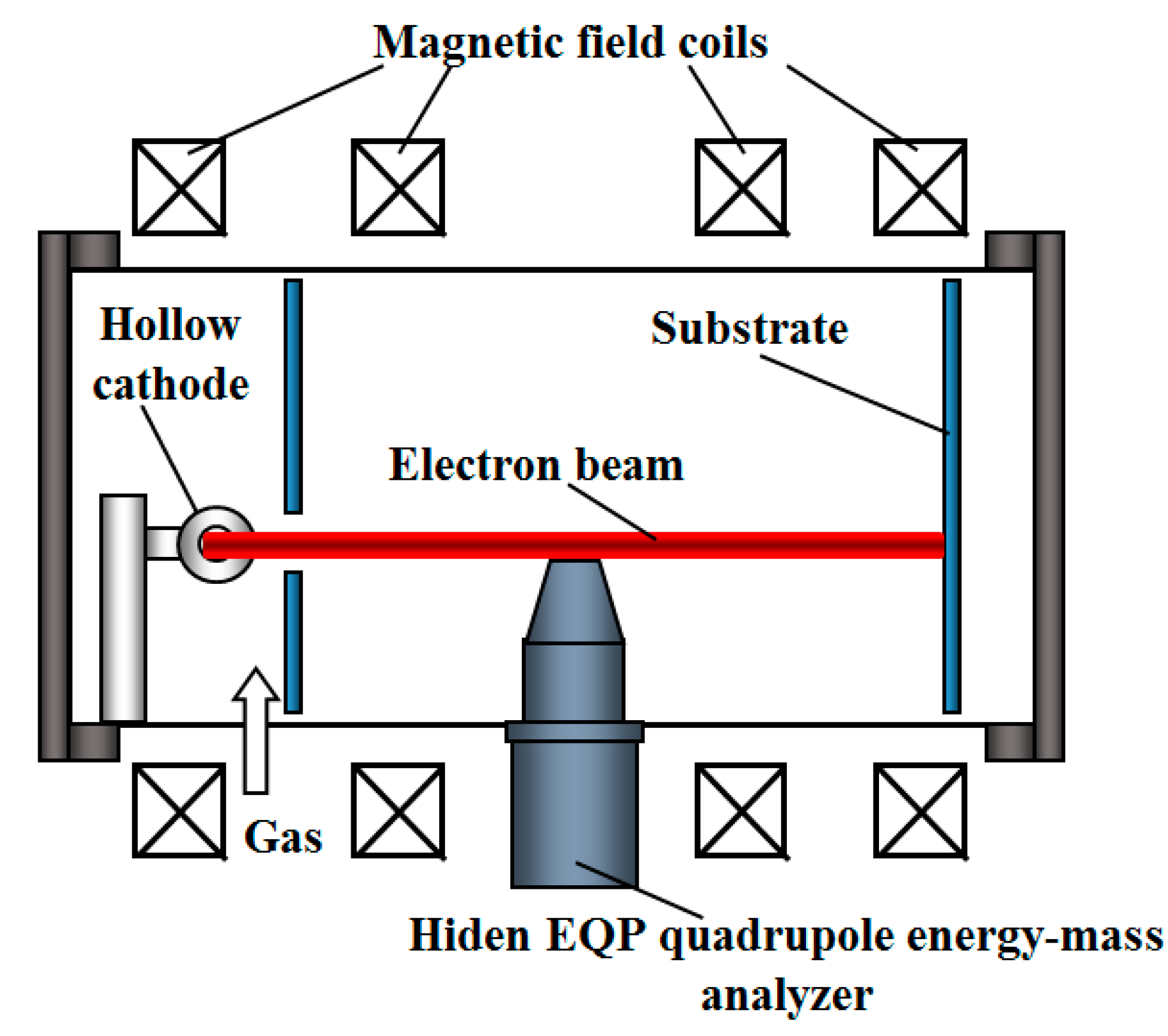
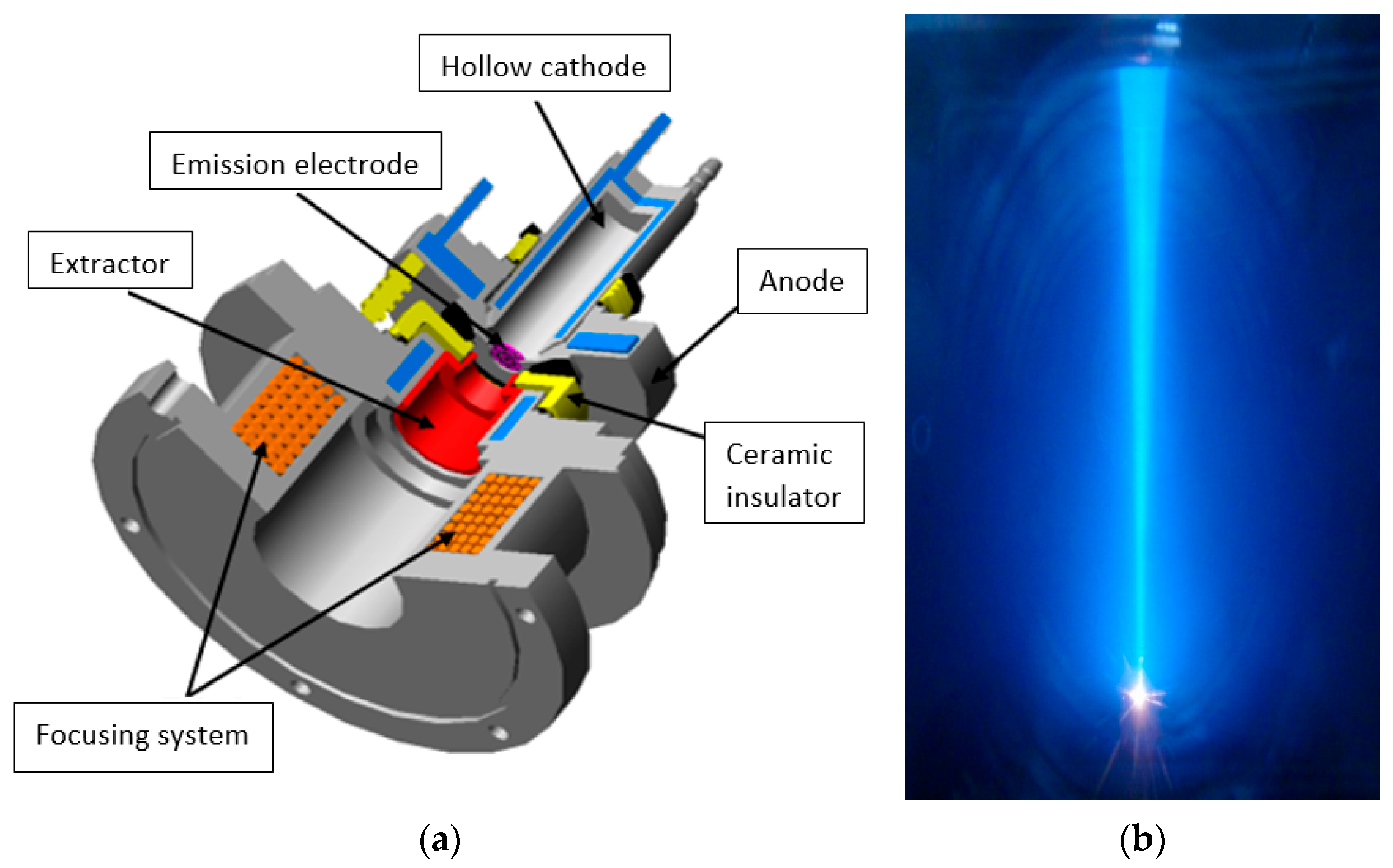
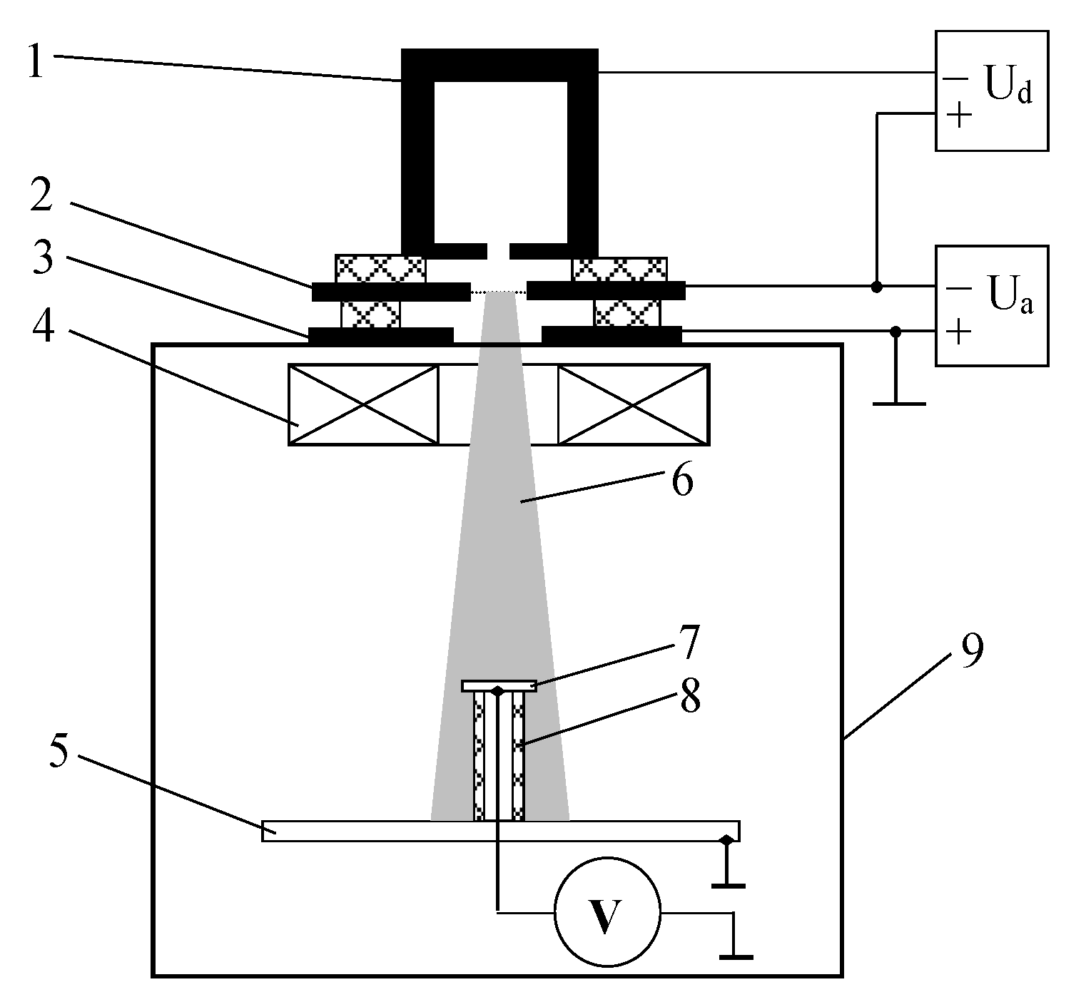
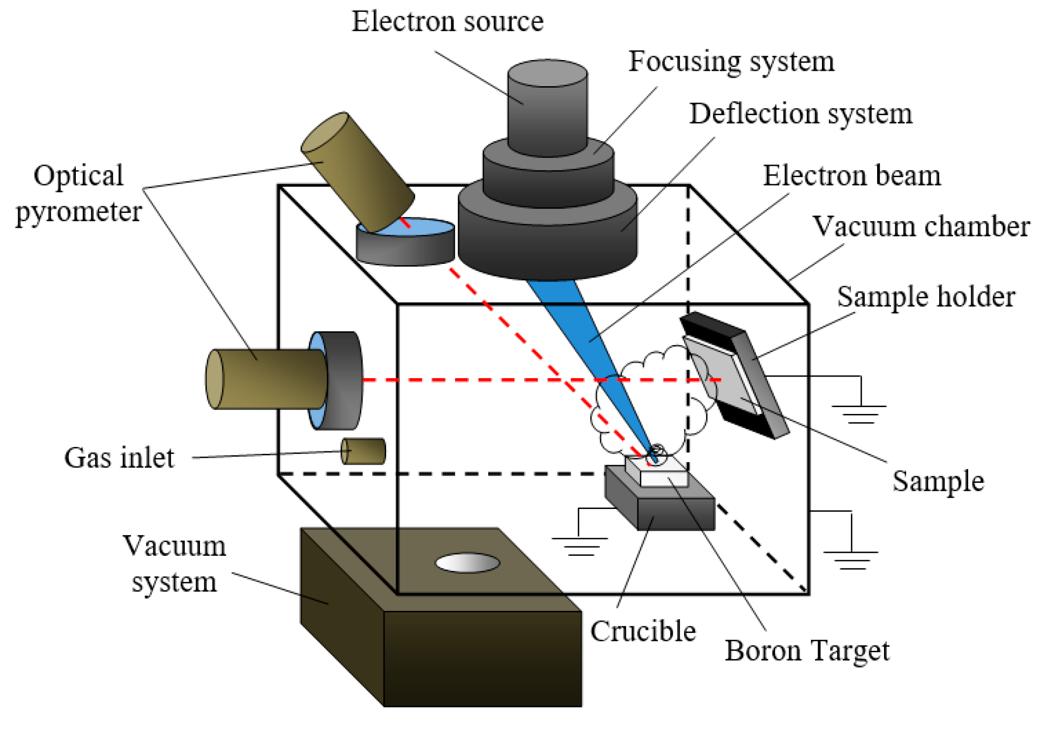
3.1. Forevacuum Plasma Electron Sources: Basic Principles of Operation

The so-called forevacuum plasma electron sources represent a modern development trend of electron sources, based on the emission of electrons from the low-temperature plasma [101]. Sources of this type provide efficient generation of electron beams in the previously inaccessible range of elevated pressure from a few to over a hundred of pascal [102]. The move to the region of higher pressure values needs to consider the operation of discharge-emission plasma electron sources and solve a number of scientific and engineering problems related to the stable work of electron sources with the electron-beam parameters that are attractive for real-world applications.
Unlike for conventional plasma electron sources, for forevacuum plasma electron sources, it is virtually impossible to create a pressure drop between the region of the emission plasma generation and the beam formation regions. Besides, the parameter pd (p—pressure, d—the gap length) for the accelerating gap of forevacuum plasma electron sources is closer to the minimum of the Paschen curve, which significantly increases the probability of gap breakdown. Note also the fact that in the region of elevated forevacuum pressure, the effect of a parasitic high-voltage glow discharge in the accelerating gap and the back ion flux from the beam plasma on the generation of the electron beam is significantly stronger [103].
The problem of the stable generation of an electron beam by a forevacuum plasma electron source in the isobaric regime has been successfully solved by creating special conditions for effective synthesis of emission plasma in the discharge system and simultaneous suppression of ionization processes in the regions of electron acceleration and beam formation. Thus, to form focused continuous electron beams at an elevated pressure, which are most suitable for electron-beam evaporation of materials, forevacuum plasma electron sources make use of a hollow cathode glow discharge for generation of emission plasma [104]. Electrostatic confinement of electrons inside the cathode hollow provided, as a result of their multiple oscillations, a high rate of ionization and, consequently, a high electron emission current density from plasma. The use of plane-parallel accelerating gap, whose electrodes are placed at a minimal possible distance from each other, restricted ionization processes in the gap to a great degree and significantly increased its dielectric strength [101]. Additionally, to ensure a high dielectric strength of the accelerating gap, forevacuum plasma electron sources use specially designed accelerating systems [101] that inhibit the breakdown along the so-called “long paths” and diminish the effect of the back ion flux from the parasitic high-voltage glow discharge and beam plasma.
The electrode diagram of a forevacuum plasma source of a continuous electron beam based on a hollow cathode glow discharge [101] is shown in Figure 12.
The hollow cathode of the discharge system of the plasma electron source is made of stainless steel; its diameter is 15–30 mm and length 40–60 mm. The flat anode is also made of stainless steel. Electrons are extracted from the plasma through an emission window of a diameter of about 10 mm cut in the anode. To stabilize the plasma emission surface and ensure the stable operation of the electron source, the emission window is draped with a fine-structured tungsten grid with high geometric transparency, or a perforated tantalum electrode is used. The electron beam is focused by a magnetic lens.
In the operational pressure range of the forevacuum plasma electron source, a hollow cathode discharge current can amount to 1.0–1.5 A at a burning voltage of 500–600 V. As of today, maximal parameters of the forevacuum plasma electron source of a continuous focused electron beam based on a hollow cathode discharge are as follows [105,106]:
-
Accelerating voltage up to 30 kV;
-
Beam current up to 450 mA;
-
Beam power up to 10 kW;
-
Power density up to 106 W/cm2;
-
Operating pressure up to 100 Pa (argon), 160 Pa (helium).
The attained electron-beam parameters of the forevacuum plasma electron source are of almost the same level as those of conventional plasma electron sources that operate in the pressure range of one or two orders of magnitude lower than the forevacuum. This makes it possible to use electron sources of this type for thermal treatment of various materials. As will be shown below, forevacuum sources are unique in that they are capable of directly processing materials with low electrical conductivity; this includes melting and evaporation of high-temperature ceramics for the purpose of dielectric coating deposition.

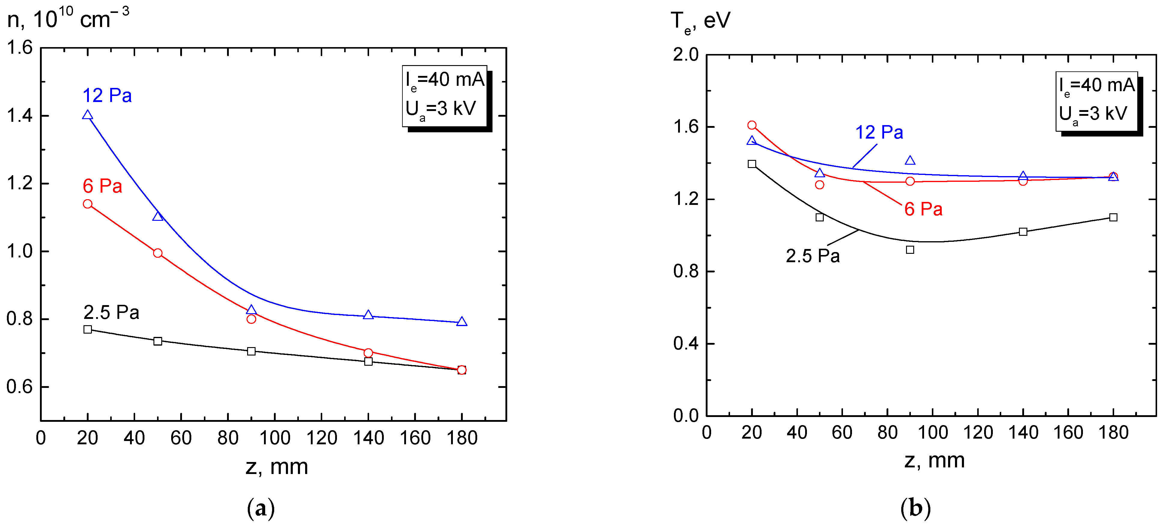
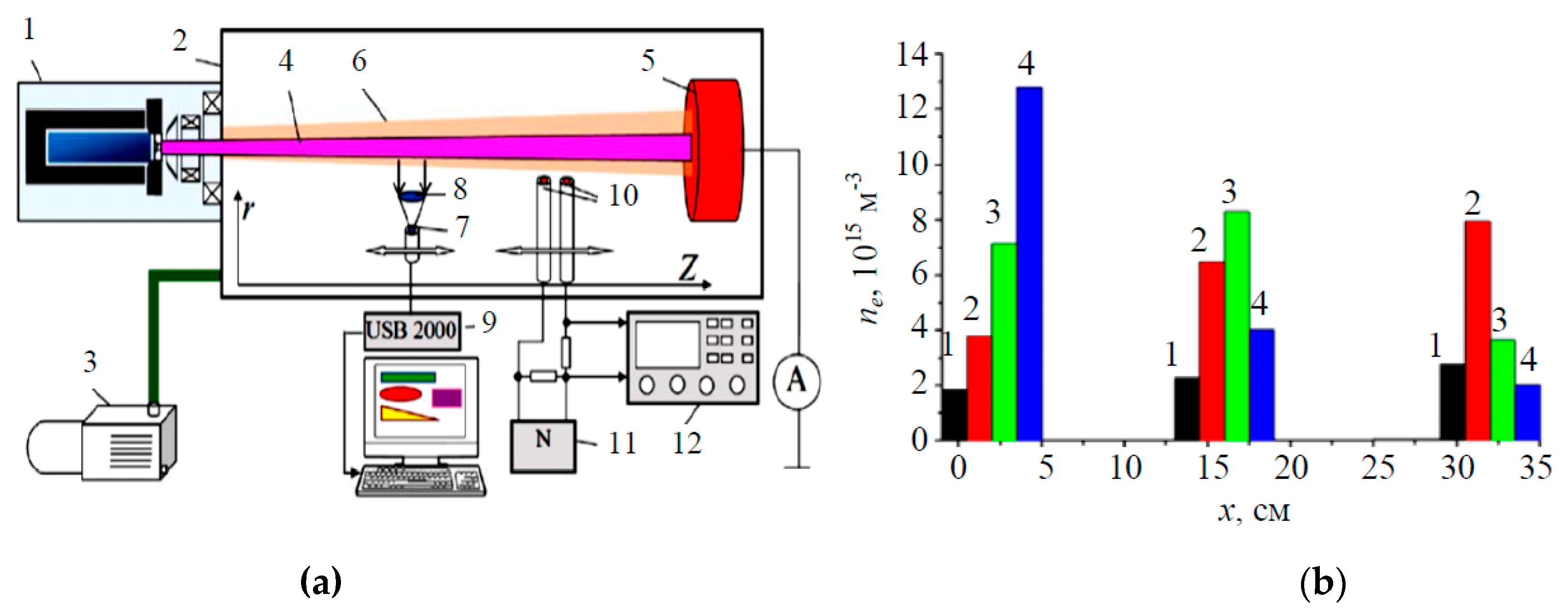
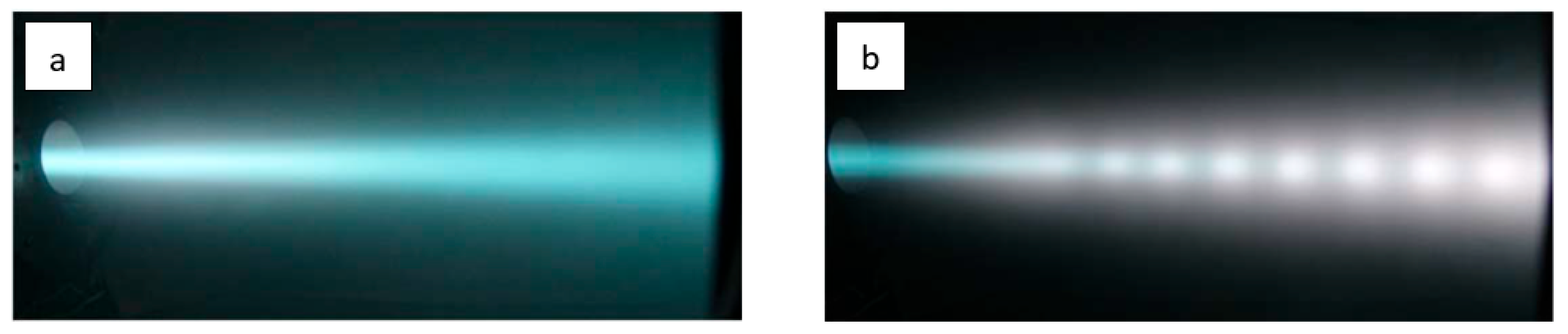
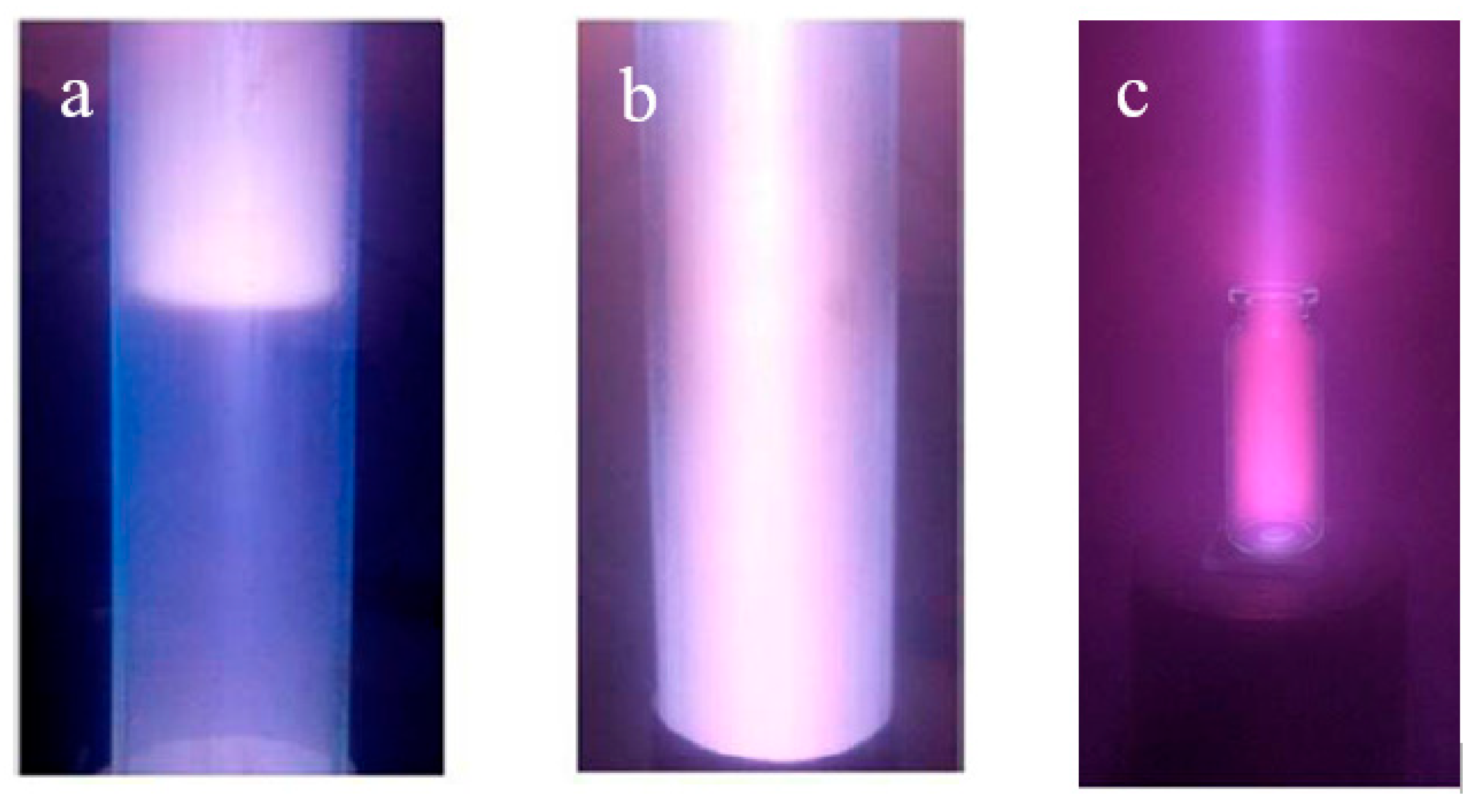
3.2. Beam-Plasma Parameters and Characteristics

Low-temperature plasma finds a plethora of technological applications, such as plasma-chemical synthesis, coating deposition, modification of materials, sterilization of medical tools and instruments, etc. [107]. Plasma is usually generated in a certain type of gas discharge. To achieve the required plasma parameters in the gas discharge and be able to vary them within a wide range is quite a complicated task. This is due to the fact that the ionization processes in a gas discharge and the related steady-state plasma parameters, first of all, provide the stable burning of the discharge at a given current. Control over the plasma parameters by varying the discharge current is in many cases accompanied by a change in the discharge burning voltage, which determines the temperature of plasma electrons and thereby their ionization capacity. The burning voltage is also affected by the pressure and type of gas, by the presence of a magnetic field, and by a number of other factors. This all produces a disproportional influence of the current and external conditions of discharge burning on the discharge plasma parameters and thereby hinders the control over the plasma parameters.
Generation of plasma by an electron beam provides wider control over the plasma parameters. This is not only because the beam current and the accelerating voltage, which determines the electron energy, can be varied independently. It is fundamentally important that the beam-plasma parameters do not significantly affect the characteristics and parameters of the electron beam.
The maximum working pressure of conventional thermal emission or plasma cathode electron sources is limited by a level of 10−1 Pa [101]. At such a pressure, the possibilities of effective generation of beam plasma are limited. The move to the region of higher pressure requires creating special conditions for the pressure separation of the regions of the electron-beam formation and transport.
The advent and development of the so-called forevacuum plasma electron sources [101] that can form stable beams at a pressure of 1–100 Pa in an atmosphere of various gases, including chemically active oxygen, nitrogen, and others, made it possible to effectively generate a beam plasma and use it for ion-plasma surface modification of various materials, polymer, and ceramics [108]. As noted in [109], practically important parameters such as plasma concentration, ion flux, and energy, as well as the plasma potential relative to the working chamber walls, directly depend on the basic plasma parameters: The electron temperature Te and concentration ne. For this reason, experimental studies of the dependence of these parameters on the experimental conditions are of great importance.
Paper [110] reports the measurements of the electron concentration and temperature of the beam plasma generated during a free propagation of a beam with energy of 3 keV in the chamber with argon at a forevacuum pressure of 2–13 Pa (Figure 13).
The plasma concentration decreases along the beam propagation direction for both low (2.5 Pa) and higher pressure (12 Pa). Despite the concentration fall, the electron temperature (Figure 13b) weakly depends on the longitudinal coordinate. As noted in [111], a relatively weak change in the temperature may be caused by high thermal conductivity of electron gas. It is shown in [112] that the beam-plasma concentration increases with increasing beam current and its energy.
Paper [113] discusses the dependence of the electron temperature on the plasma concentration and on the beam energy recorded at a fixed position of a single Langmuir probe, Figure 14.
The results shown in this figure demonstrate a noticeable increase in the plasma concentration with an increase in the beam current. This can be related to the proportional dependence of the ionization on the beam current [114]. A smooth growth of the electron temperature with increasing beam current, as noted in article [108], may be related to a general increase in the fraction of the high-energy plasma electrons due to an increase in the concentration of beam electrons. It should be noted that the plasma concentration and electron temperature virtually do not depend on the beam energy (Figure 14b). The authors of [115] showed that with an increase in the pressure from 1 to 15 Pa, at a fixed current of about 30 mA and beam energy of up to 5 keV, the beam-plasma concentration increases, while the electron temperature decreases. Their calculations demonstrated that the cooling of plasma electrons, even disregarding inelastic collisions, mostly occurred through collisions with neutral molecules. The predominant mechanisms through which plasma electrons lose their energy are collisions with gas and the heat transfer from plasma by the electron flux. Thus, in the forevacuum pressure range of 1–15 Pa, using a focused electron beam, it is possible to create a plasma with a temperature of about 1 eV and a concentration of 109–1010 cm−3, the parameters of which can be controlled by several independent quantities: The beam current and energy, the pressure, and the type of gas.
Paper [116] reports the experimental studies of the spatial distribution of the concentration and temperature of electrons of the beam plasma created by a continuous ribbon electron beam with energy of up to 2 keV in an argon atmosphere at a pressure of 6 to 9 Pa. The electron beam, formed by the forevacuum plasma electron source, had a cross section of 10 mm × 250 mm. When propagating in the argon medium, the beam created a plasma which was confined in the electron-beam propagation region by creating a longitudinal magnetic field. It was demonstrated that the distributions of the electron concentration and temperature directly depend on the related distribution of the current density over the beam cross section, and the plasma parameters are essentially affected by the pressure in the vacuum chamber. Thus, with increasing pressure, the beam-plasma concentration increases to amounts up to 1010 cm−3 at a current density of 15 mA/cm2. A similar increase occurs with increasing beam current. The magnetic field strength affects the cross-section width of the “plasma sheet”. With increasing voltage, the plasma cross-section width decreases and simultaneously its concentration in the middle beam plane increases.
The parameters of the beam plasma, generated by a forevacuum plasma electron source of a ribbon electron beam with an energy of 2 keV and a beam size of 10 cm × 1 cm, transported without a magnetic field at a pressure of 5–10 Pa, are given in [117]. Unlike the case of plasma generation in the presence of a magnetic field [116], two beam-plasma interaction regimes are possible here. At relatively low beam currents (150–200 mA), the beam propagation in the transport region is characterized by a low concentration of the beam plasma (about 5 × 10¹⁵ m−3) and a low electron temperature (0.5 eV). A twofold increase in the beam current brings about a significant increase in the electron concentration and temperature, up to 1.5 × 10¹⁶ m−3 and 2 eV. The increase in the concentration is accompanied by an enhanced plasma glow [118]. Paper [119] presents the measurements of the parameters of the beam plasma generated during the propagation of a focused electron beam with an energy of up to 15 keV and a beam current of up to 300 mA in a helium atmosphere at a pressure of up to 50 Pa. The schematic diagram of the setup and the distribution of plasma concentration is shown in Figure 15.
It has been demonstrated that the position of the region of intense interaction between the electron beam and plasma can be controlled by varying the beam current density, which is achieved by changing the position of the beam crossover. In the absence of a crossover, i.e., when the beam electrons move towards the collector along almost parallel trajectories, the concentration of plasma electrons varies weakly along the propagation path. By changing the beam focusing parameters and placing the crossover near the collector (at a distance of about 2 cm), or in the middle between the collector and the electron source, or near the electron source, one can observe in the corresponding area a maximum of the plasma electron concentration: The plasma concentration in this area increases by three times or more compared to the propagation of a uniform beam without a crossover (Figure 15). This article also demonstrates another effect related to the interaction of an electron beam and plasma: The formation of alternating bright and dark bands in the beam-plasma glow (Figure 16). The alternating bands were observed along the beam axis for a relatively narrow range of the beam parameters: at a beam current close to 200 mA, an accelerating voltage range of 8–14 kV and the beam crossover position of 5–7 cm from the collector (Figure 16b).
The observed phenomenon resembles strata, i.e., static or movable fringes of uneven luminosity alternating with dark bands in the positive column of a low-pressure gas discharge [120,121]. As noted by the authors in [119], the observed alternation of dark and bright bands, similar to strata, exists in a very narrow interval of the beam current and electron energy and may be related to the emergence of beam instability.
Injection of an electron beam into a dielectric cavity under high vacuum conditions is only possible if the negative charge brought by the beam is removed [122]. The use of forevacuum plasma electron sources allows one to bypass this physical limitation. The possibility of generating beam plasma entirely in a dielectric space has been demonstrated in [123], which reports the measurement of parameters of the beam plasma created during the injection of an electron beam into a cylindrical thin-walled quartz bulb with an inner diameter of 4 cm and a length of 20 cm (Figure 17). Experimental studies of the parameters of the generated beam plasma showed that the plasma potential inside the vessel was negative and increased with increasing pressure; and the beam-plasma concentration in the vessel was found to exceed the concentration of the plasma created by the beam in the free space of the vacuum chamber. In an earlier paper [124], it has been shown that there exist operational modes, in which the plasma occupies the entire space of the cavity even in the absence of any electrodes to remove the electric charge inside. In this case, the current is closed by a reverse flux of secondary electrons from the cavity surface, as well as through the beam plasma to the grounded parts of the vacuum chamber. It has been found in [124] that there exist generation regimes in which the plasma takes up the dielectric volume only partially (Figure 17a). With increasing pressure, the plasma fills the entire volume (Figure 17b). In addition, it has been shown for the first time that varying the gas pressure and the energy of the injected beam changes the character of the longitudinal distribution of the plasma concentration. With optimal parameters, the non-uniformity of concentration can be reduced to about 10% [118].
The increased concentration has been explained based on the developed numerical model [125,126], which incorporates a numerical balance model that explains the increased concentration and the temperature of the beam-plasma electrons in the dielectric cavity by the additional energy contribution of secondary electrons knocked out by the beam electrons and plasma ions from the inner cavity surface and accelerated in the near-wall and near-bottom layers. It has been shown that the contribution of secondary electrons to ionization sharply increases in the gas’s lower range of pressure, whereas the contribution of plasma electrons remains negligibly small. Thus, the beam plasma in a confined space can be used for sterilization of medial glass and plastic bottles and vials (Figure 17c) [127].

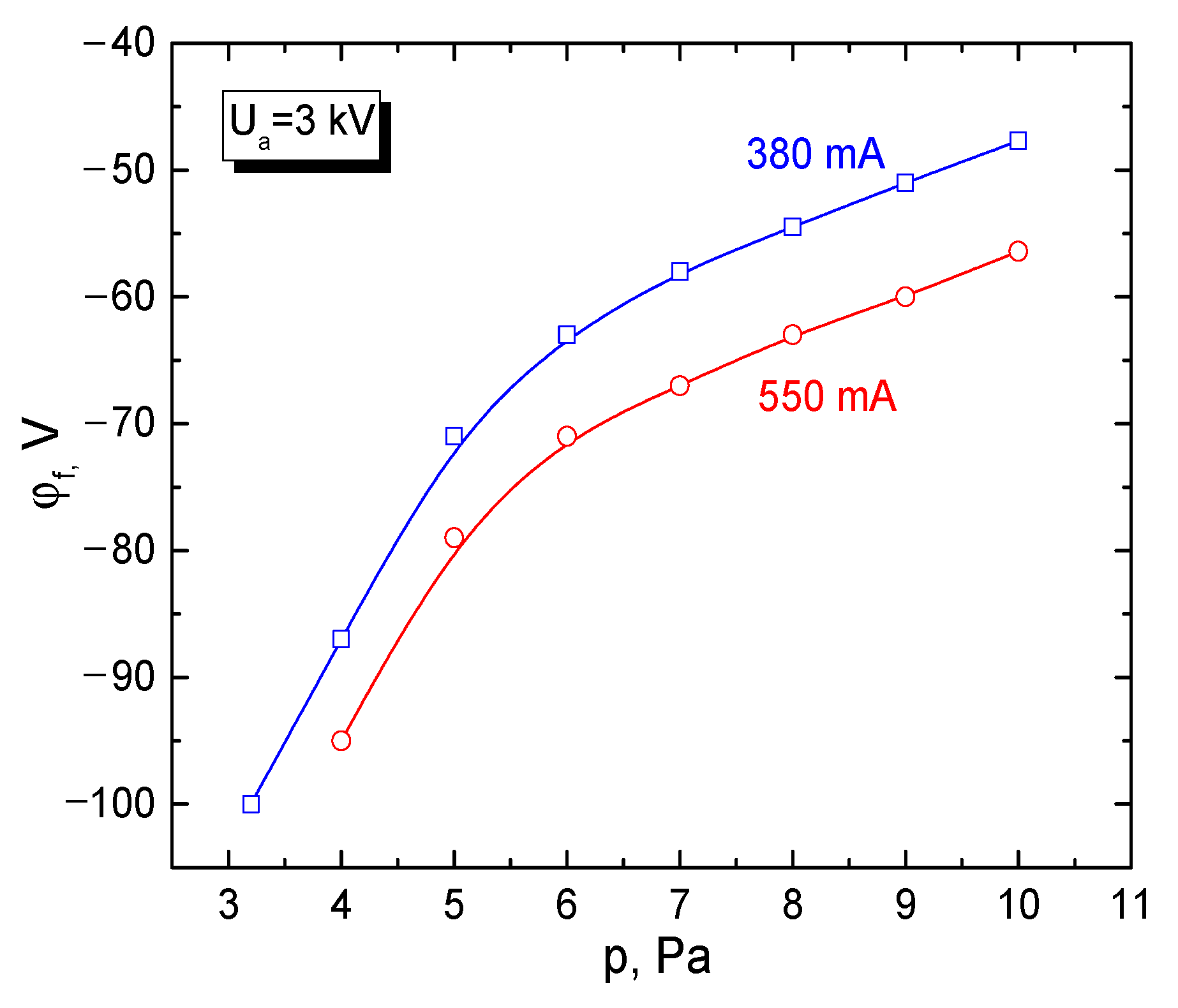
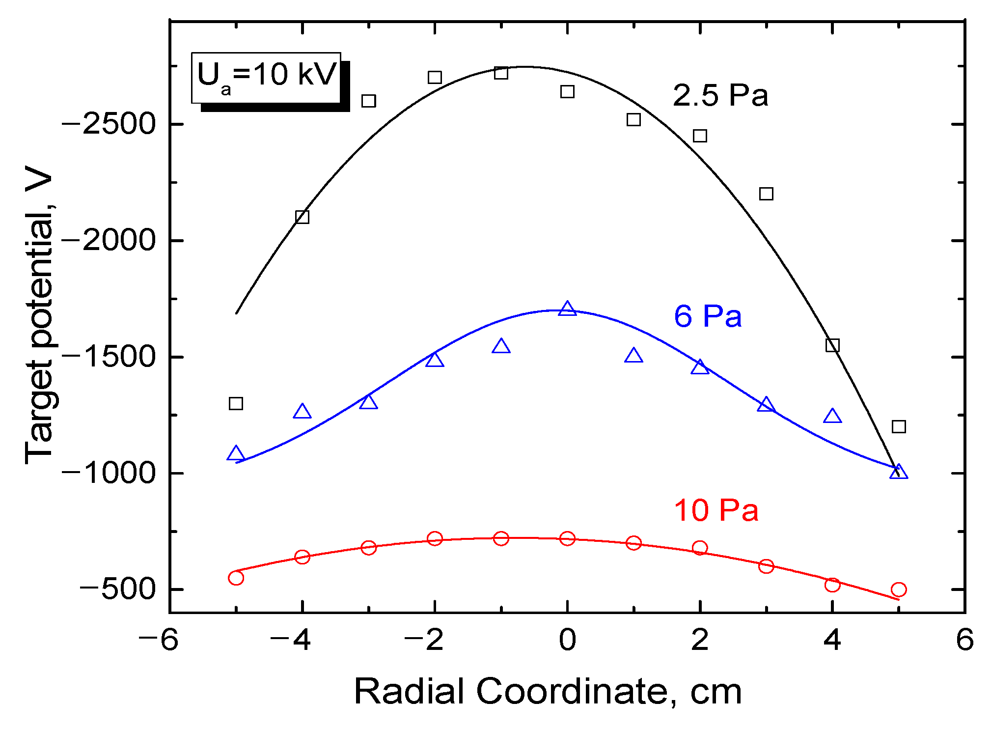
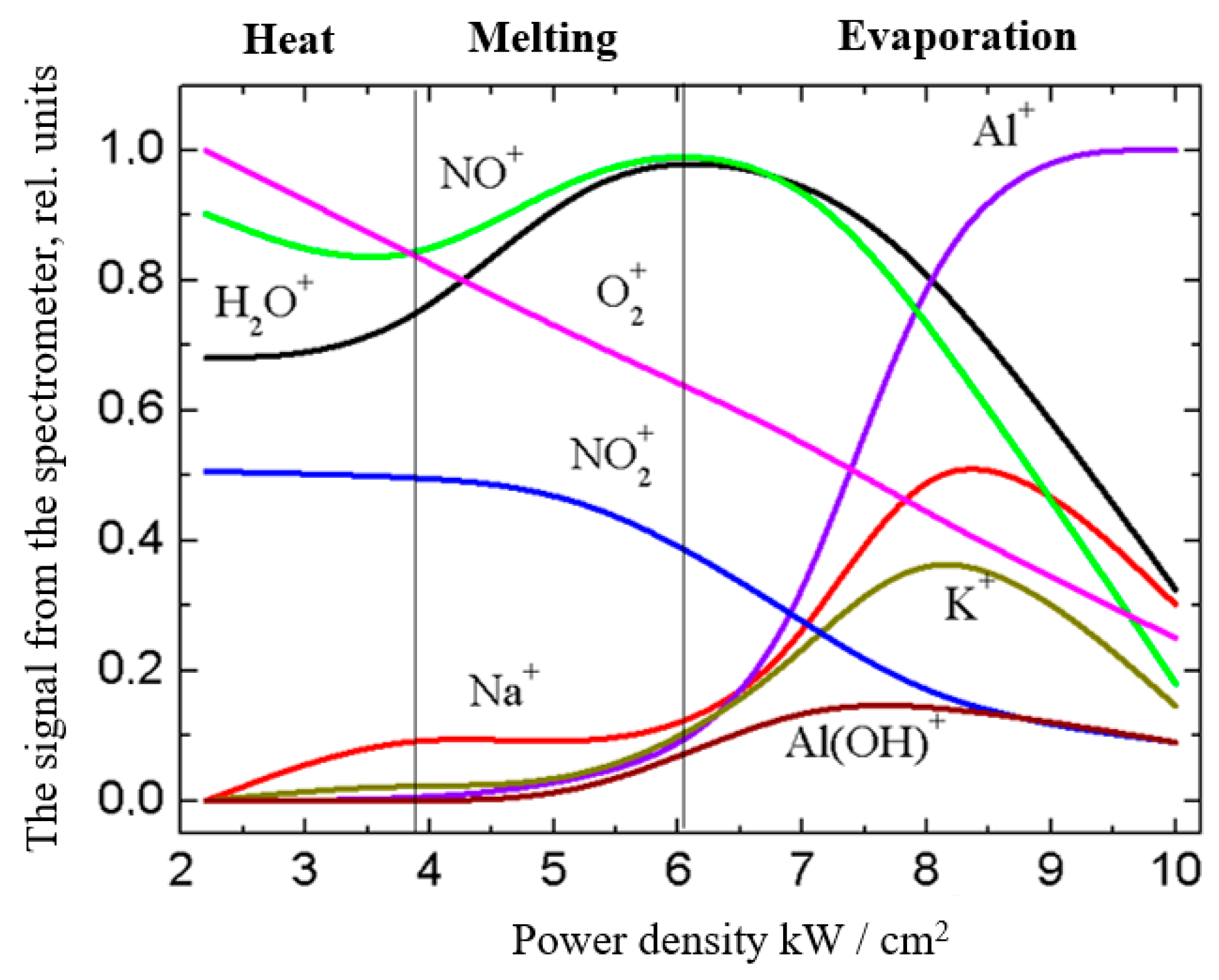
3.3. Potential of a Dielectric Target Irradiated by an Electron Beam in Forevacuum

The beam plasma generated in the forevacuum pressure range, during the transport of the accelerated beam, can neutralize the electron-beam charging of electrically non-conductive surfaces (dielectrics). We modeled the plasma neutralization of the dielectric surface in the experiments on the electron-beam interaction with an insulated metal target [128]. The experimental setup is shown in Figure 18.
The key question set in in the experiment was to determine the steady-state potential of the insulated metal target irradiated by electrons. Electron beam 6 was generated by a forevacuum plasma electron source, whose electrode scheme consisted of hollow cathode 1, flat anode 2, and accelerating electrode 3 [101]. Magnetic lens 4 was used to focus the electron beam. The focused electron beam hit the insulated stainless steel target 7. The target steady-state potential relative to the grounded collector and the vacuum chamber was measured using a high-resistance voltmeter.
In all experiments, the measured potential of the insulated metal target irradiated by the electron beam remained negative. As expected, the steady-state value of this potential increased with increasing electron-beam current and energy of accelerated electrons (Figure 19). At forevacuum pressures, the gas pressure is the predominant factor that diminishes the absolute value of the target potential [129].
As seen from the experimental dependences in Figure 19, already at a pressure of 10 Pa, under irradiation by an electron beam with an energy of 3 keV, the absolute value of the steady-state potential of the insulated target dropped down to 60–50 V. In the pulsed mode of operation of a forevacuum plasma electron source, at significantly higher electron-beam currents (for a microsecond pulse the electron-beam current amounts to tens of amperes), the absolute value of the potential is significantly higher and can reach 2500 V at an accelerating voltage of about 20 kV [130]. Note that according to experiments, at lower pressures, the electron beam charges the insulated metal target almost to the full magnitude of the accelerating voltage.
Thus, for the forevacuum pressure range, and all cases of the electron-beam action, the steady-state potential of the insulated metal target is either close to zero (low-current continuous electron beam) or much less than the accelerating voltage (high-current pulsed electron beam).
We have found from analysis of experimental data, theoretical estimates, and numerical modeling that in the forevacuum range, the steady-state potential of an insulated target is affected by the electron-beam parameters, and by the ion current to the target and secondary electron emission from the target surface [131]. An important additional factor that contributes to an increase in the ion flux to the insulated target is the discharge ignition between the negatively charged target and the vacuum chamber walls. In this case, the current of the discharge circuit closes via the electron beam. The discharge ignition manifests itself as an increase in the plasma glow in front of the insulated target, is accompanied by an increase in the plasma concentration in this area, and leads to a further decrease in the absolute value of the target potential [132].
When estimating the value of the steady potential of a dielectric target irradiated by an electron beam, one should account for a non-uniform distribution of the potential over the dielectric surface, as well as for the difference in the coefficients of secondary electron emission between metal and dielectric. Since the direct method of measuring the potential on a dielectric surface is virtually impossible, this potential was determined using indirect methods [133]. Thus, for measuring the potential on the alumina ceramic surface, a set of flat copper probes with a diameter of 3 mm was inserted into the dielectric target with a diameter of 30 cm [133]. The results for the target irradiated by an electron beam are shown in Figure 20. As follows from the data in Figure 20, the potential distribution over the surface of the dielectric target is non-uniform and, at the low-pressure value of forevacuum, the maximum value of the potential of a few kV is comparable to the accelerating voltage of 10 kV. However, a relatively slight increase in the pressure noticeably smoothens the potential distribution and significantly decreases the absolute value of its minimum.
At a pressure as low as 10 Pa, the potential decreases to 700 V and almost compares with the case of the insulated metal target irradiated by an electron beam. As in the case of insulated metal target, an increase in the discharge current and in the accelerating voltage brings about the corresponding increase of the absolute value of the dielectric target surface potential. However, in this case, the potential stays well below the accelerating voltage that determines the electron energy.
Thus, the generation of dense beam plasma during the electron beam transport in forevacuum provides mostly complete neutralization by ions of the electron beam charging of the surface of an electrically non-conductive target. The charge compensation enables one to directly subject dielectric materials to the electron-beam processing, including the synthesis of dielectric coatings by electron-beam evaporation of dielectric targets.

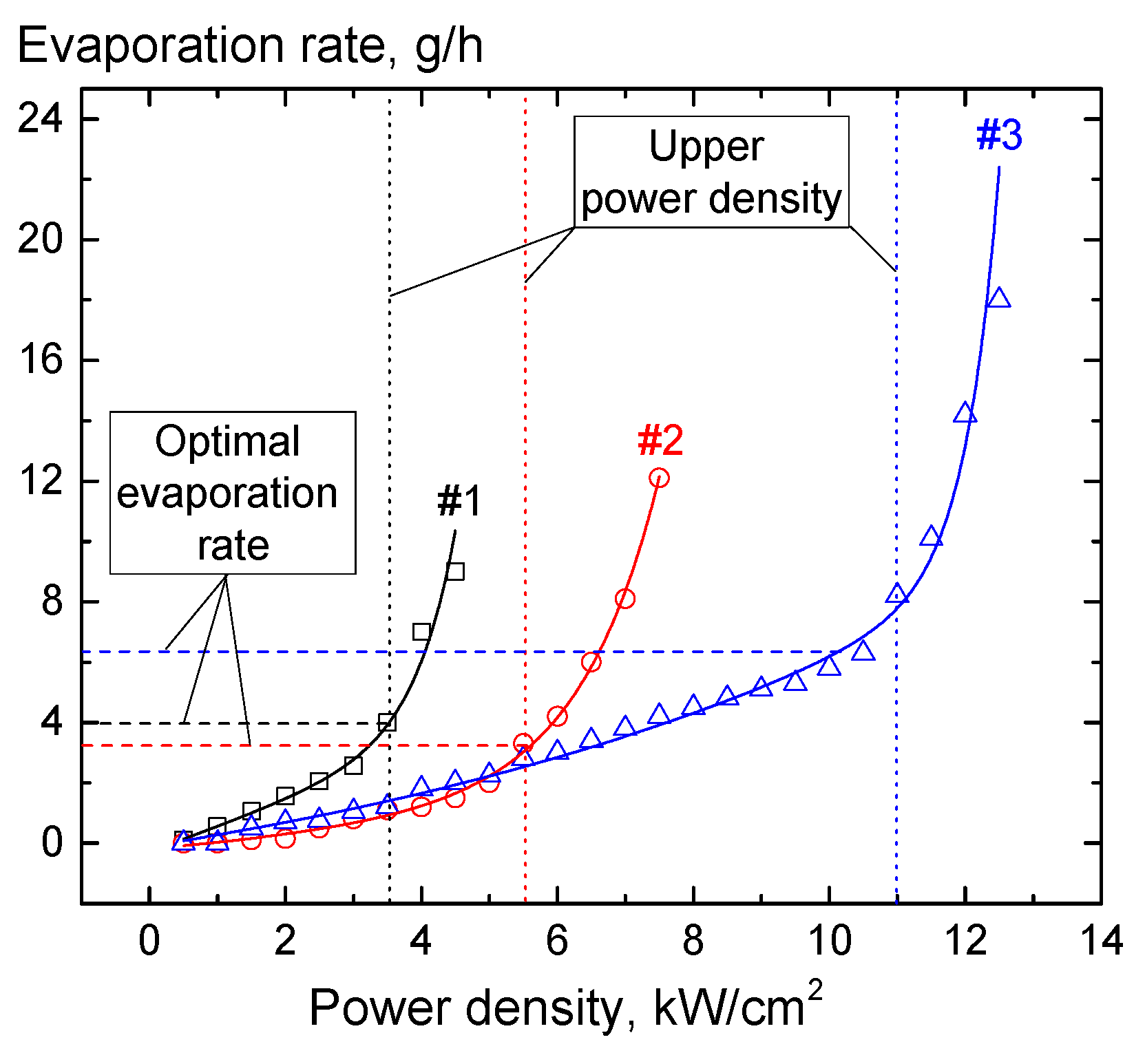
3.4. Parameters and Characteristics of Dielectric Coatings

Electron-beam synthesis of dielectric coatings relies on using an electron beam for heating and evaporation of a dielectric target, followed by the deposition of evaporated products on the workpiece surface. As has been noted above, direct electron-beam evaporation of materials with low electrical conductivity can be implemented with the help of forevacuum plasma electron sources. In this case, the beam plasma generated by electron-beam evaporation can provide the ion-plasma assistance in coating deposition, while the use of chemically active gases as a working medium can affect the composition and structure of coatings and, therefore, their properties and parameters. The choice of optimal parameters of an electron beam is connected with thermal properties of the evaporated material of the dielectric target. The electron-beam optimal parameters, as well as thermal regimes of the electron-beam exposition, may greatly differ for different target materials. In this section, the electron-beam synthesis of dielectric coatings is presented using examples of the evaporation of alumina ceramics, boron, and silicon carbide.

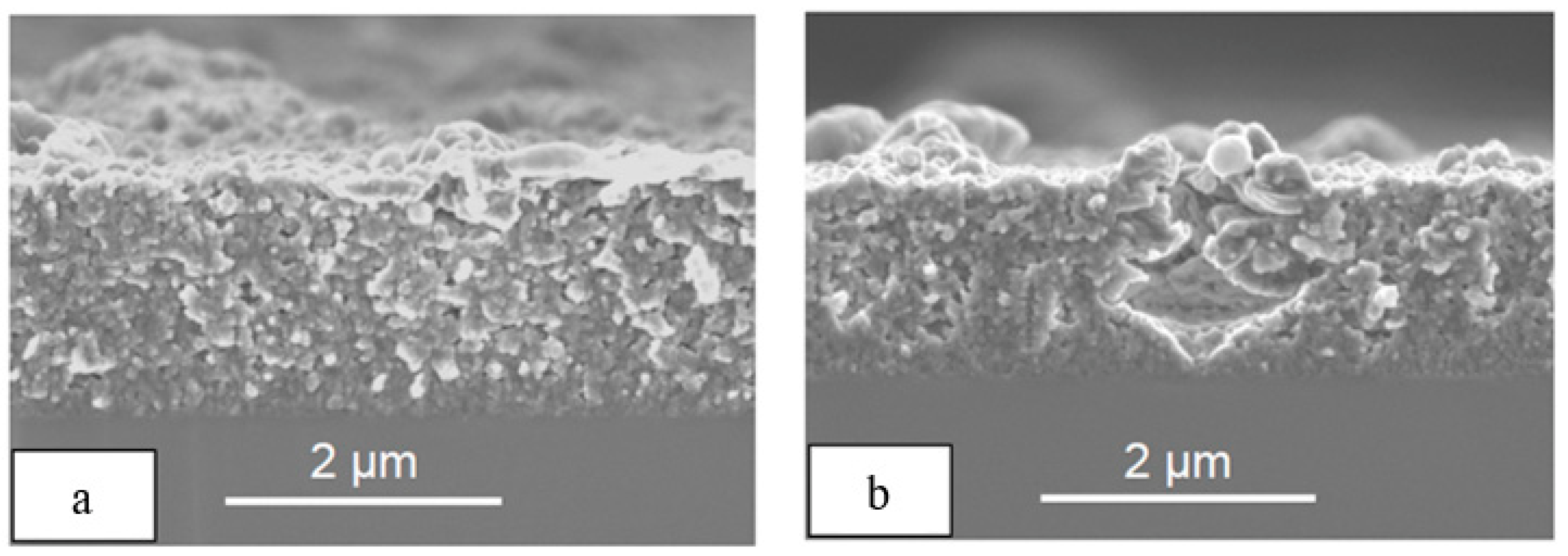
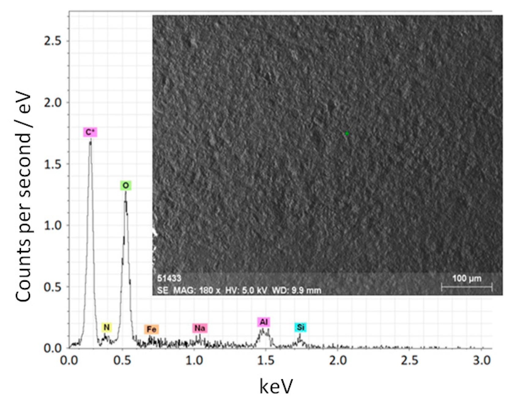
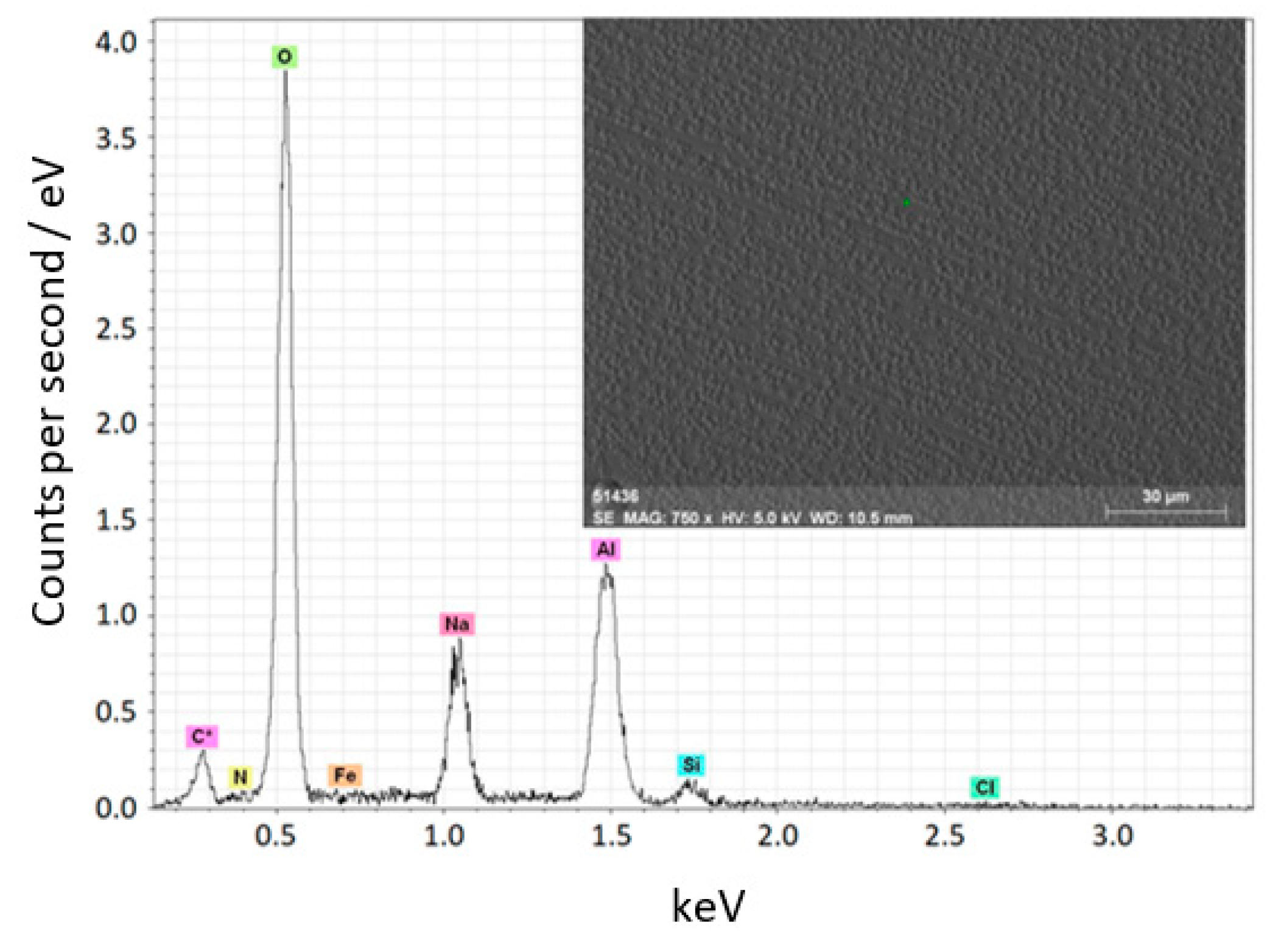
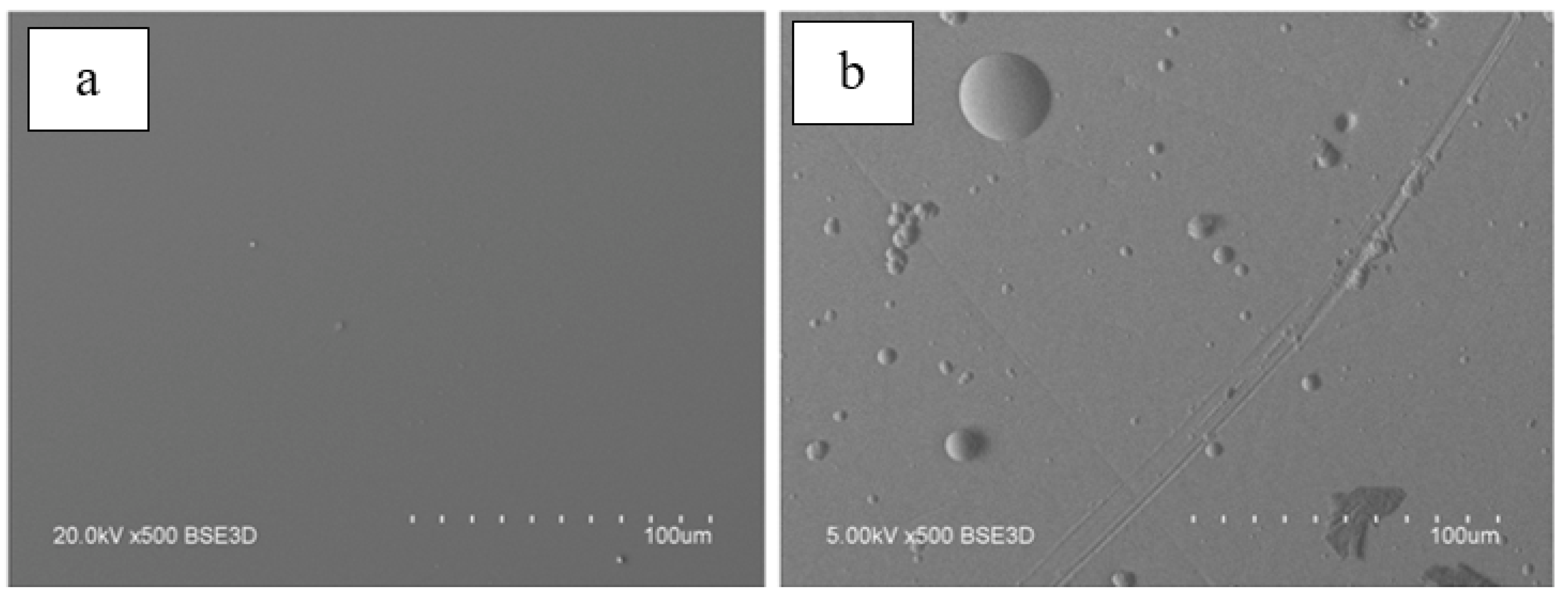
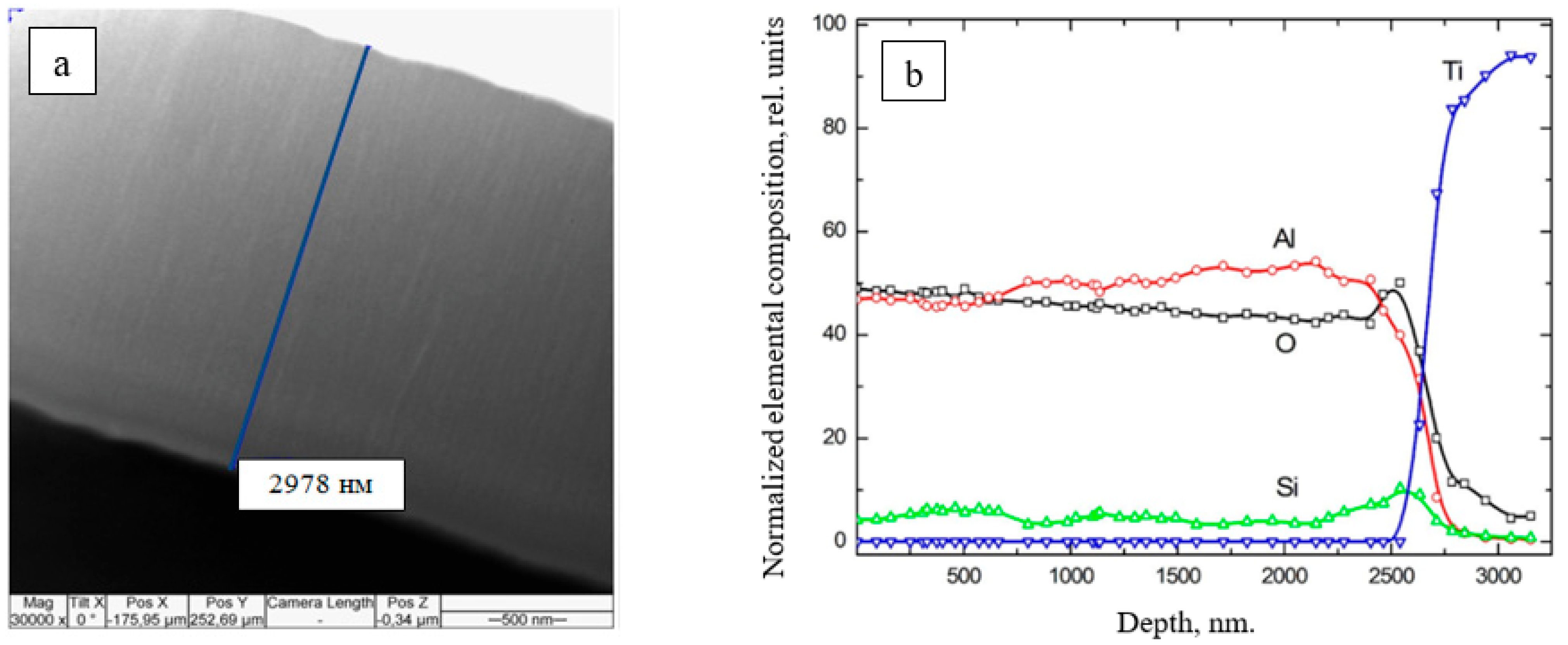
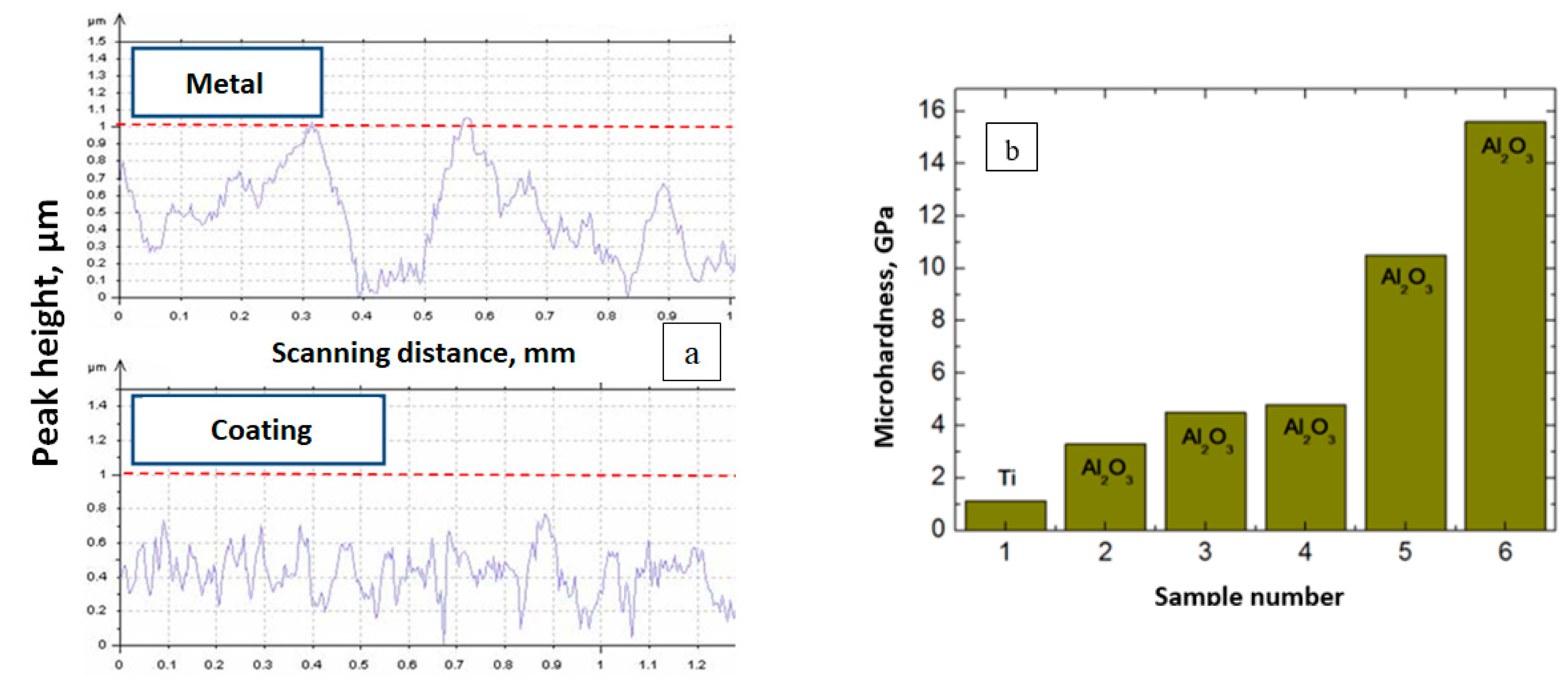
3.4.1. Ceramic Coatings

Let us consider the process of heating, melting, and evaporation of a dielectric target using the example of aluminum oxide ceramics. An electron beam with a current of 150 mA and energy of up to 20 keV was focused on a diameter of 4 mm on a ceramic target (a cube with an edge of 1 cm). The evaporated ceramic sample, besides aluminum and oxygen, contained impurities of sodium, nitrogen, iron, silicon, and carbon (Figure 21). The ceramic cube was placed in a tantalum crucible. In the process of the electron-beam heating of the ceramic target, plasma was created nearby, which contained, together with the ions of the gas atmosphere, the ions of the evaporated material. The fraction of ions of the target material directly depends on the electron-beam power [134].
Using the experimental dependencies in Figure 22 of the ion composition on the electron-beam power density, one can see how the beam-plasma composition is changing during heating, melting, and evaporation of the ceramic target throughout the entire process of deposition (in this case, the entire cycle takes up to 1 min) [10]. At relatively low values of the beam power density (p = 2–4 kW/cm2) and accordingly of the electron-beam power during the ceramic sample heating, the sodium and potassium peaks in the mass spectra increase, together with the growth of the energy of the bombarding particles. The presence of these elements is due to their content in the raw materials, feldspars, used to manufacture ceramics, and because of their low molar heat of evaporation (Na—98 kJ/mol, K—77 kJ/mol) and a lower boiling point (Na—882.95 °C, K—773.85 °C) compared with aluminum (284.1 kJ/mol, 2518.85 °C). As a result, sodium and potassium are the first to evaporate from the surface layer of the ceramics into the vacuum chamber space. Relatively low values of ionization potentials of these elements (Na+—5.14 eV, K+—4.3 eV) provide effective ionization.
With a further increase in the beam power density from 4 to 6 kW/cm2, the ceramic sample melts. In this range of power density, no noticeable change in the ion composition of the “ceramic” plasma is observed, and the amplitudes of sodium and potassium peaks remain at the same level. At a power density of above 6 kW/cm2, the sample temperature is high enough for evaporation and ionization of aluminum and its compounds. The peak amplitudes of sodium and potassium increase, which may be related to the evaporation of these elements from the bulk of the sample. At a power density of above 6 kW/cm2, the spectra show a sharp increase in the peaks of the elements contained in the ceramics. In this case, the peaks of the “ceramic” plasma ions begin to dominate over the “gas” plasma ions, which is indicative of the increased concentration of ceramic ions in the regions of registration of the beam-plasma ions and the substrate location. The peaks of the sodium and potassium curves at a beam power density of 8 kW/cm2 can be related to the evaporation of all additives used in the ceramic manufacture. At an electron-beam power density above 8.5 kW/cm2, the peaks of aluminum ions dominate the spectra [10].
Figure 23 shows micrographs of the ceramic coating and its elemental composition. As seen, the elemental composition of the coating deposited on the substrate almost matches the composition of the ceramic target (see Figure 21). The ratios of the components in the evaporated target and in the deposited coating differ.
The experimental results in Figure 24 distinctly show two regions with a relatively slow and a faster increase in the rate of the target material evaporation with increasing electron-beam power. In the first case, the increase in the evaporation rate can be related to an increased temperature in the melt pool, as well as with the expansion of the pool’s area. In the second region, the sharp increase in the evaporation rate is connected with intense boiling of the material in the melt zone with the formation of the droplet fraction in the evaporated flux. Each of the ceramic target samples has a threshold power density at which a noticeable droplet fraction with a characteristic drop size of up to 20 µm appears. Depending on the composition of alumina ceramics and its thermal physical properties, the threshold power density for the appearance of the droplet fraction ranges from 1 to 10 kW/cm2. The presence of droplets in the evaporated flux degrades the quality of coatings. For this reason, the maximum electron-beam power density in the electron-beam synthesis of dielectric coatings must be restricted. It appears that the threshold value of the electron-beam power density for a particular evaporated material is a physical limitation imposed on the possibility of obtaining uniform ceramic coatings using the electron-beam evaporation in forevacuum. The target evaporation at a power density below the threshold enables one to form a uniform film on the substrate surface (Figure 25a).
At the maximum possible electron-beam power of 10 kW/cm2, the target evaporation rate is 5 g/h. With the electron-beam power density being the decisive factor that affects the evaporation rate, the coating thickness is normally controlled only by the process duration. In this case, it should be taken into account that for intensive evaporation, different ceramics must be heated up to different temperatures. Table 3 shows the coating thickness for evaporation of alumina ceramics of different compositions and corresponding deposition rates.
The obtained rate of the electron-beam deposition of ceramic coatings falls short of the characteristic values for electron-beam evaporation of metals. Nevertheless, it is much higher than that for the alternative method of magnetron sputtering of dielectric targets.
Figure 26 shows a photograph of a cross-section of a ceramic coating on a titanium substrate and the distribution of the elemental composition with the sample depth [135]. The high uniformity of the coatings and the absence of pores are connected with the high migration ability of the coating atoms at a high substrate temperature (over 700 °C) due to radiation heating. The high substrate temperature stimulates the formation of the crystal structure of coatings with the presence of Al2O3 γ- and α-phases. It should be noted that the elemental composition is constant with the depth, which is indicative of stability and uniformity of the deposition process.
The surface profile of this coating is shown in Figure 27. As seen, the roughness amplitude of the original sample is about 1 µm, and after the coating deposition, diminishes to 0.8 µm, which is over 20%. The width of non-uniformity peaks also decreases by over 60%, which indicates that the roughness of the sample surface reduces (Figure 27a) [135].
The maximum micro-hardness amounts to 16 GPa, which almost matches the micro-hardness of aluminum oxide ceramics (Figure 27b). The coatings synthesized from the impurity-free ceramics possess the highest hardness. Such coatings have the most pure elemental composition, with only traces of oxygen and aluminum, and possess a granular surface structure. They also have higher Young’s modulus, though with an increased surface roughness.
Comparison of the electrical insulating parameters of the coating with those of the evaporated target material indicates their proximity (Table 4).
One of the application examples of such dielectric coatings is their use of a heat sink from the integrated circuit surfaces [136].

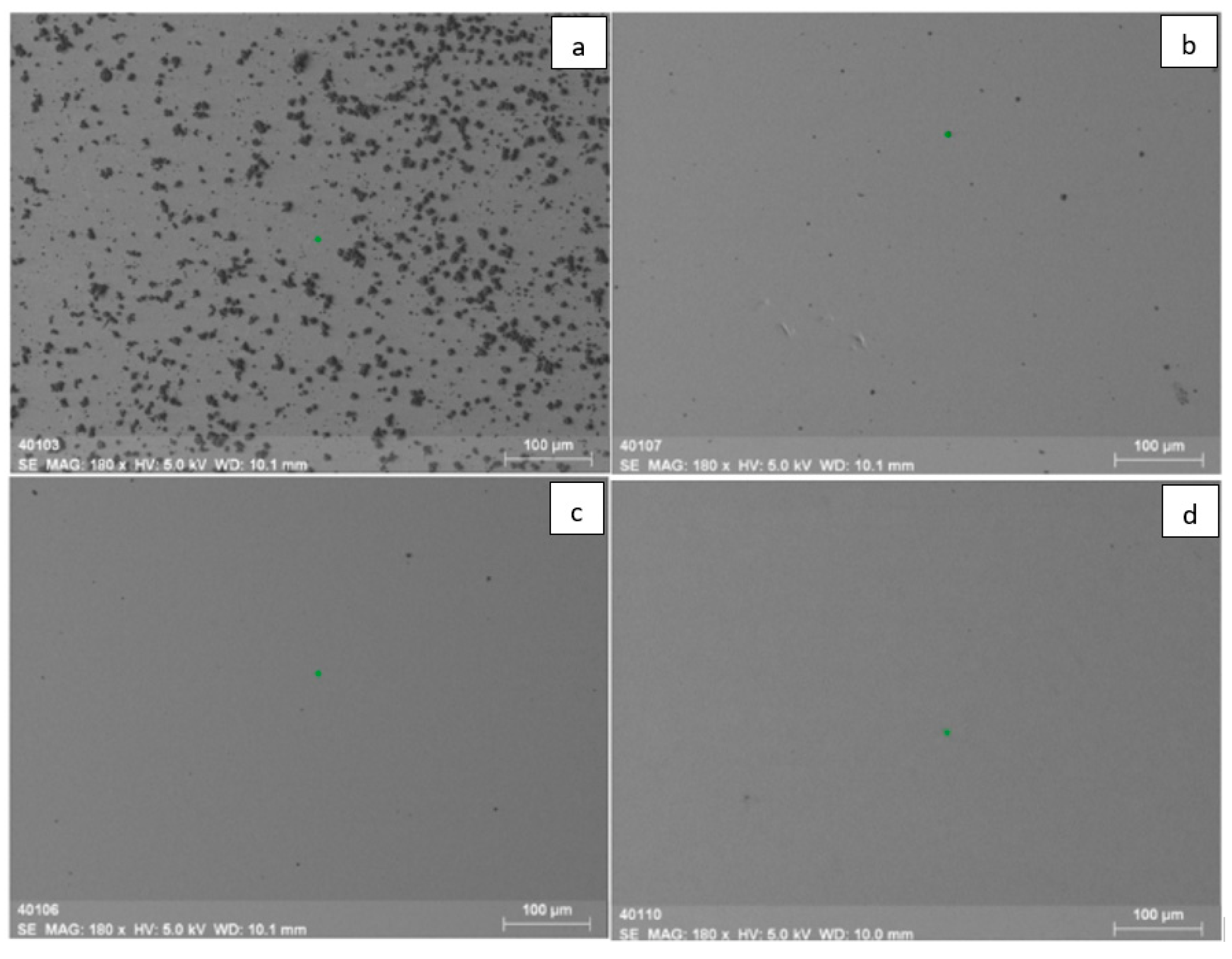
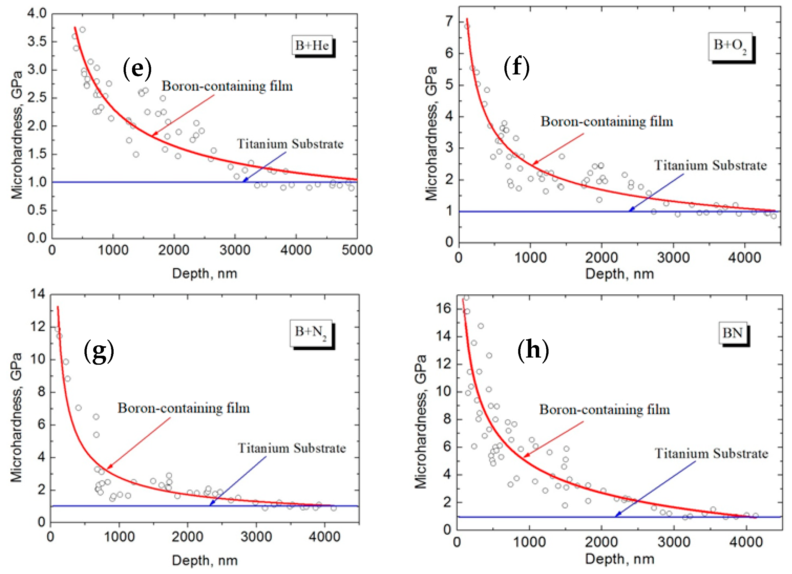
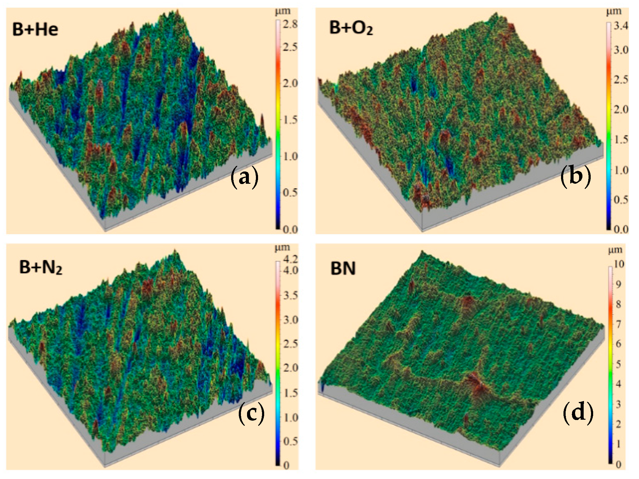
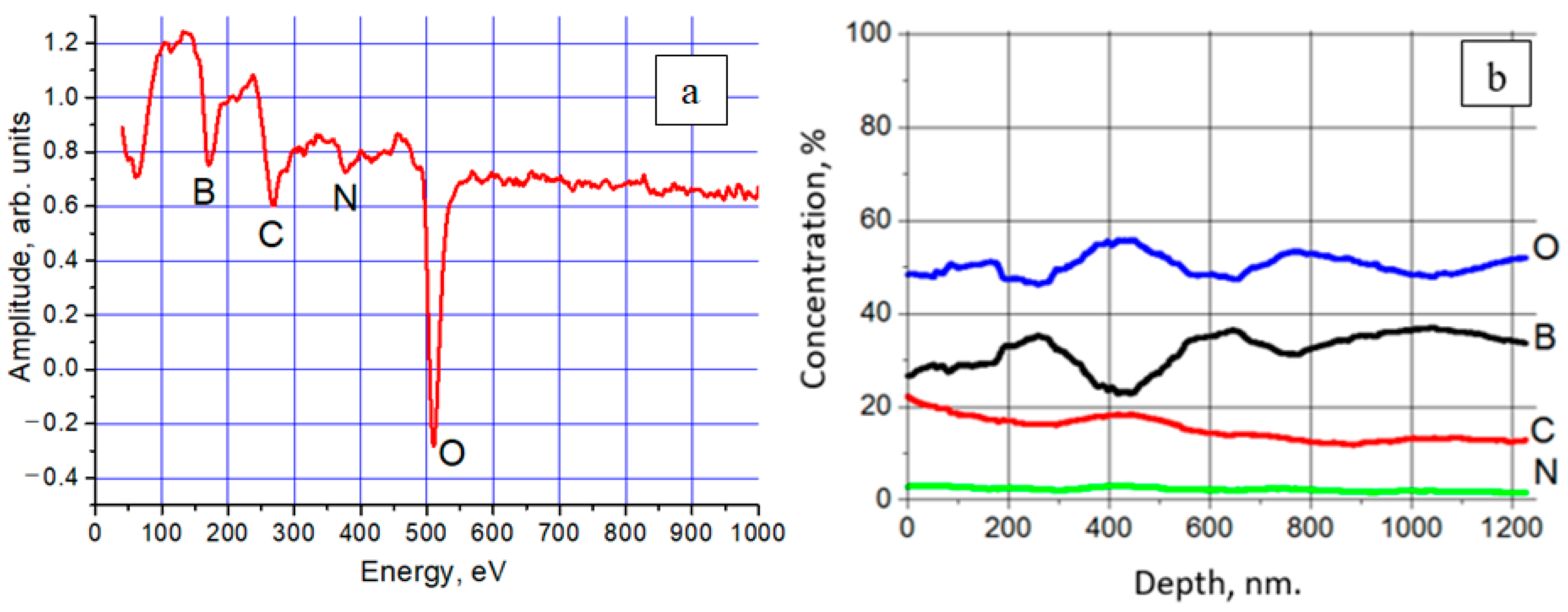
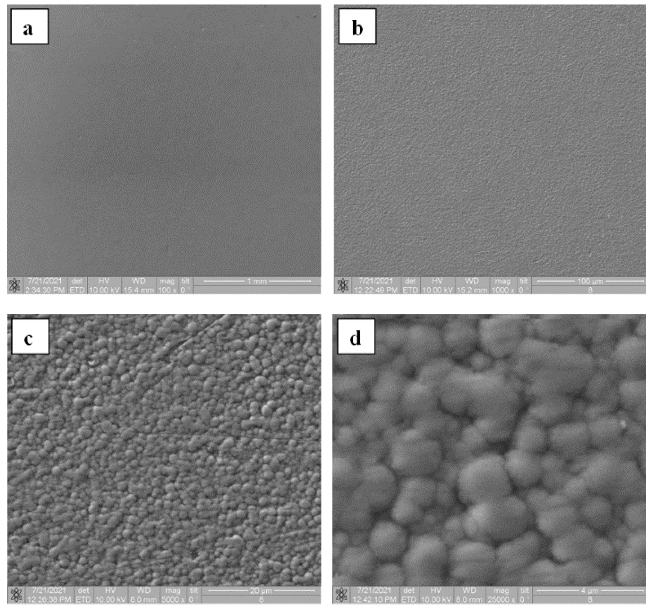
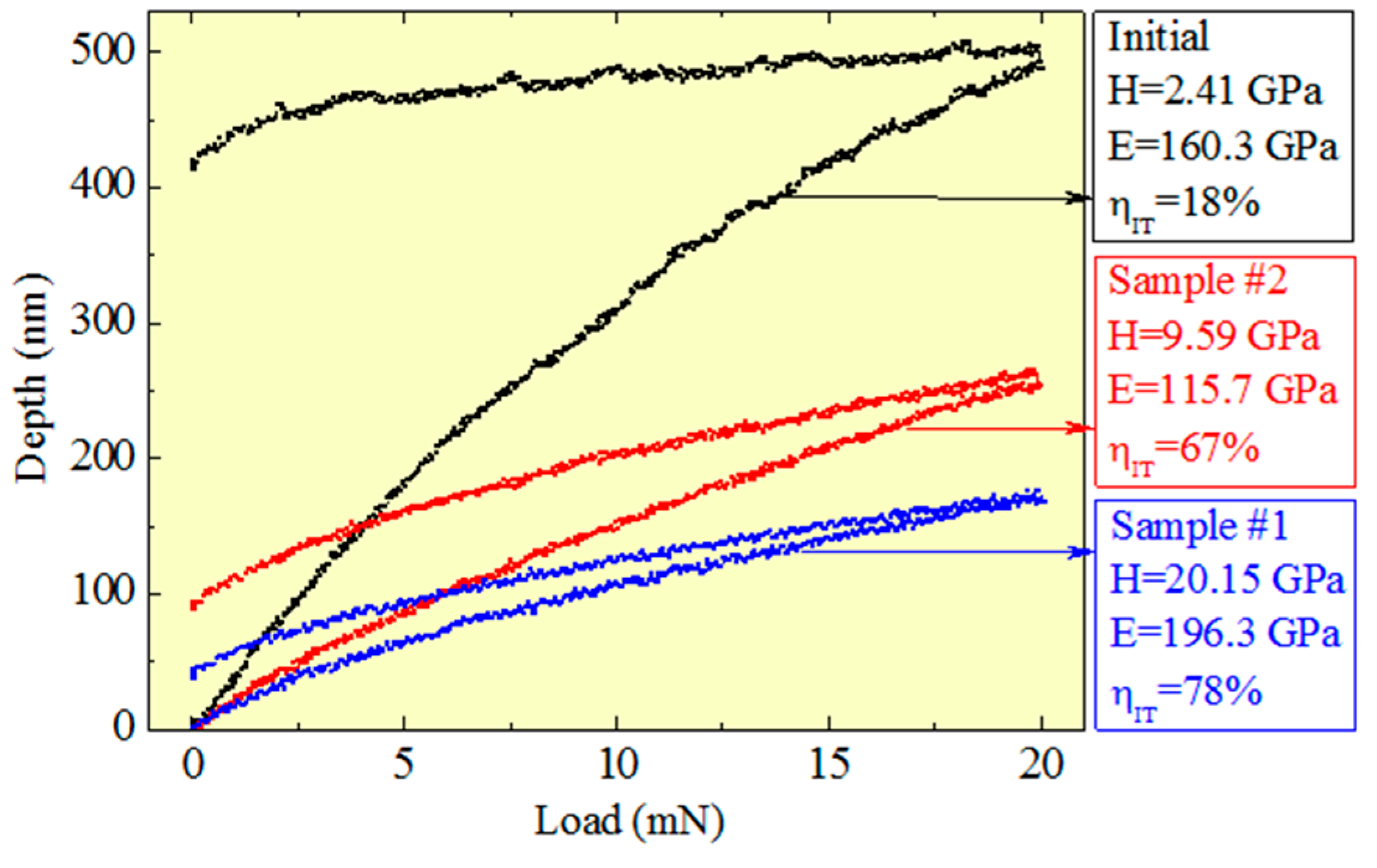
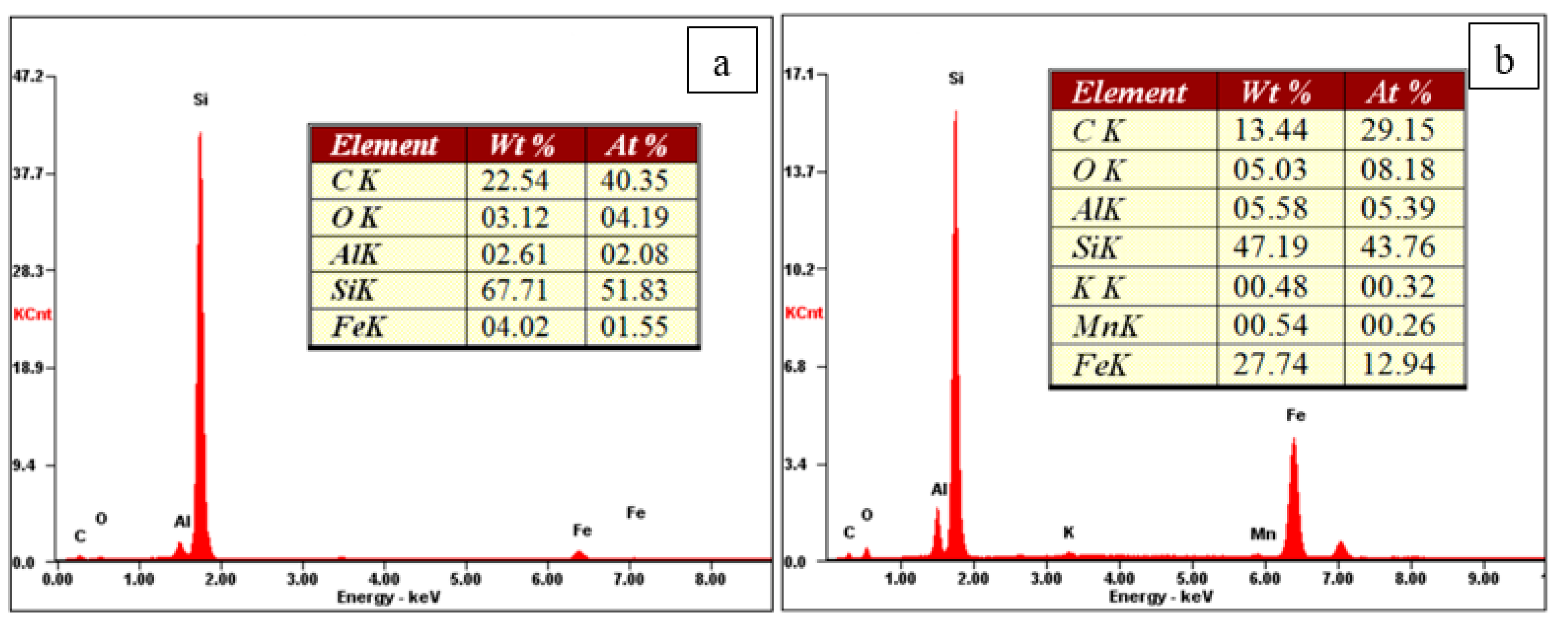
3.4.2. Boron-Containing Coatings

Plasma with a high content of boron ions can be effectively generated and used for coating deposition by evaporation of a boron-containing target using a continuous focused electron beam of a forevacuum plasma source at a pressure of about 10 Pa. One of the specific features of boron at room temperature is its high electric resistivity (~106 Ω·cm). This resistivity drops sharply with increasing temperature. So, one should expect certain peculiarities of electron-beam evaporation of a boron sample regarding this feature, which should be taken into account when selecting the optimal evaporation regime for the synthesis of boron-based coatings.
A typical experimental setup for electron-beam evaporation of pure crystalline boron and boron nitride is shown in Figure 28 [137]. The electron source provided the generation of an electron beam with a current of up to 200 mA and energy of 1–20 keV. As a rule, the experimental cycle includes three stages. First, an electron beam of 100 mA and an accelerating voltage of up to 5 kV heats up the target to prevent it from cracking due to thermal stress. Then, the accelerating voltage slowly rises from 1 to 10 kV. When the critical electron-beam power is reached, the target begins to melt, and at a beam current of 200 mA and an accelerating voltage of 15–20 kV, the solid-body target evaporates, with the target temperature at this point being about 2500 °C.
The temperature dependence of the boron target on the electron-beam power density is shown in Figure 29 [138].
The duration of the entire process was 5 to 20 min depending on the target composition (B or BN). Simultaneously with the deposition of coatings, it was possible to monitor the mass-to-charge composition of the beam plasma using a modified RGA-300 quadrupole mass-spectrometer [139,140]. Figure 30 shows photographs of the obtained boron-based coatings at different electron-beam power densities, and the distribution of micro-hardness with the depth of the coatings deposited during evaporation of boron and boron nitride in different gases. The data in the graphs allow one to indirectly determine the coating thickness. Since all graphs in the plots reach “saturation” at a pressure of ~1 GPa, which corresponds with the known tabular value of titanium Vickers micro-hardness (1 GPa), one can estimate the thickness of the coatings obtained from boron nitride in an atmosphere of different gases to be 3.5 µm. The thickness of the coating synthesized from boron in the residual atmosphere amounts to 5 µm.
The conducted studies have shown that, despite approximately the same thickness, the boron-based coatings deposited in a gas medium, unlike boron nitride coatings, follow the substrate surface profile. There are visible long scratches left by the initial polishing of titanium substrates. As seen from the 3D surface profiles (Figure 31), the boron-based coatings deposited in different gas atmospheres contain many ridges and depressions. Their surfaces accommodate elements of a needle-like structure with a size of 0.1–0.5 µm, which can be caused by local chipping and destruction of thin surface layers due to internal stress.
The presented profiles show that for the boron-based coating, the maximum profile height is 2.5 µm in the helium atmosphere, and about 3 µm in oxygen and nitrogen; while for boron nitride it is characterized by the presence of large inclusions with peaks of about 8 µm. The typical photographs and the elemental composition of the boron-containing and boron nitride coatings are shown in Figure 32. X-ray fluorescence analysis carried out on an XRD-7000S diffractometer (Shimadzu, Japan) showed (see Figure 32 a,c) that the boron-based coatings, fabricated by electron-beam evaporation of a pure boron target in an inert gas atmosphere, contain predominantly boron and oxygen. The spectra also contain lines of the substrate material (titanium).
The presence of oxygen is connected with its content in the residual atmosphere of the vacuum chamber and on the surface of the titanium substrate, which promoted its concentration both inside and outside of the fabricated films. The peaks of titanium and oxygen prevail over the boron lines, which is indicative of small thickness of the boron-containing layer. On the contrary, for boron nitride coatings (see Figure 32b,d), there is observed the highest peak corresponding to boron and weak lines of titanium and oxygen, which indicates a sufficiently thick boron-containing coating capable of absorbing the characteristic radiation of the substrate (titanium). The small amplitude of the oxygen line can be explained by the fact that the substrate is saturated with oxygen to a greater degree than the boron-containing coating or its surface layer. The presence of a large amount of impurities (magnesium, calcium, aluminum, and silicon) is due to the production method used to manufacture boron nitride targets, where magnesium is used as a production stimulator. The impurity lines have small amplitude, which indicates their insignificant content in the fabricated coating. The small amplitude of the nitrogen line is apparently associated with high absorption of characteristic nitrogen radiation by the formed coating, so that the spectrum contains only the lines of nitrogen atoms located predominantly in the near-surface layers [141].
Qualitative analysis of the coating showed that it contains atoms of boron, oxygen, carbon, and nitrogen (Figure 33). The presence of a considerable amount of boron (about 30–35%) throughout the entire coating thickness prompts the possibility of using forevacuum plasma electron sources for electron-beam evaporation of boron and deposition of a uniform boron coating.
It should be noted that the elemental composition of the coating is constant with the thickness, which confirms the stability and uniformity of the deposition process. The absence of the substrate elements in the coating at a depth of about 1 µm and a short deposition time (1 min) are indicative of a high deposition rate. The numerical values of the coating surface parameters are summarized in Table 5.
The parameter Sq, which is more sensitive to extreme values of roughness than Sa, made it possible to reveal the presence of individual sharp rough areas distinctly seen in the layout of the boron nitride coatings. Besides, there are artifacts in the form of larger peak-like violations of the surface uniformity. The profiles with a positive asymmetry coefficient are dominated by micro roughnesses with sharp high peaks that stand out from the average height. Negative values of Ssk characterize the surfaces with sharp deep depressions, such as the surfaces of the coatings obtained in the mixture of oxygen and nitrogen. This agrees with the graph in Figure 31. The combination of kurtosis and asymmetry can identify the surfaces which have relatively uniform high and low extreme points, such as, for example, the boron coatings in helium and nitrogen atmospheres.

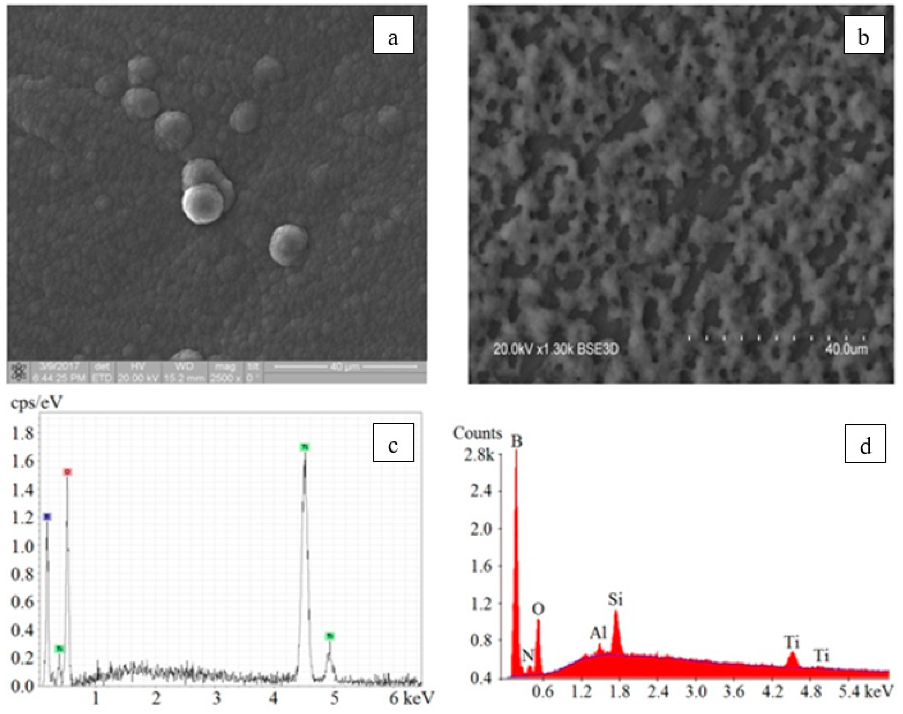
3.4.3. Silicon-Carbon Coatings

Silicon-carbon coating (film) is a set of film structures that contains silicon and carbon atoms. These coatings are of interest to researchers and engineers due to a wide range of properties: chemical and thermal resistance, high Young’s moduli, low coefficient of thermal expansion, hardness, and high wear resistance. They usually have a low coefficient of friction, which is required for various moving mechanisms, and as such, silicon-carbon coatings are used as protective coatings in cutting tools, computer hard disks, and micro-electromechanical systems [142].
The experimental setup for the electron-beam synthesis of silicon-carbon coatings in principle does not differ from the experiments for production of ceramic or boron-based coatings. A high-temperature tantalum crucible, with a silicon carbide target inside, 0.5 cm thick and 1 cm in diameter, was placed at the bottom of the vacuum chamber. The SiC targets were prepared by uniaxial pressing at a pressure of 160–800 MPa at room temperature. Micrographs of the synthesized silicon-carbon coatings are shown in Figure 34. The rate of electron-beam evaporation of silicon carbide, and hence the deposition rate, increases with increasing electron-beam power density, so in order to avoid the formation of a droplet phase, the power density in experiments was restricted to a level of 7 kW/cm2. Morphology analysis of the surfaces of deposited coatings showed that the silicon-carbon film is a structure consisting of spherical grains ranging in size from hundreds of nanometers to a few micrometers. Similar results were previously obtained in [143], where the silicon-carbon coatings were produced using electrochemical deposition. Table 6 shows the data on micro-hardness and deposition time of silicon-carbon coatings in comparison with other deposition methods. As seen, the micro-hardness of the coatings obtained by electron-beam evaporation varies from 9 to 20 GPa and almost reaches the maximum for such coatings. Note that the synthesis by electron-beam evaporation of a 1000 nm coating takes only 10 min. As follows from the data in Table 5, this time is tens of times less as compared with alternative techniques. Note also the values of Young’s moduli (Figure 35).
For the sample with a substrate temperature of 600 °C (Sample No. 1), Young’s modulus was about 200 GPa; for the sample with a substrate temperature of 300 °C (Sample No. 2), Young’s modulus was 115 GPa. Such a difference may be related to the elemental composition of the coatings (Figure 36). The coating of the sample with a higher temperature contains half as much oxygen and aluminum. These conclusions are in good agreement with the authors of [144].
Table 6. Comparison of micro-hardness and synthesis time of silicon-carbon coatings obtained by different methods.
MethodMicrohardnessDeposition Time
Kaufman ion source [145]5–12 GPa2 h
DC PECVD [146]9–17 GPa6–12 h
RF PECVD [147]13–18 GPa4–8 h
Deposition from self-sustained arc discharge plasma with hot cathode [144]6.5–20 GPa8 h
Electron-beam evaporation in forevacuum9.5–20 GPa10 min
Figure 35 shows the indenter loading curves for the original sample and for the samples with typical coatings. As seen from the figure, the obtained coatings have high values of elastic recovery, which may be indicative of an enhanced relaxation capacity of the material, especially stress relaxation under cyclic loads, which provides effective resistance to fatigue fracture [148].
Figure 36 shows the elemental composition of the obtained silicon-carbon coatings. The content of carbon ranges 30–40%, silicon 40–50%, oxygen 4–8%. It has been noticed that with an increase in the content of silicon, the hardness of coating decreases, which agrees well with the results of the authors of [144].
Figure 37 shows the results of tribological studies of the coated samples obtained at different substrate temperatures.
As seen, the synthesis of the silicon-carbon coating diminishes the coefficient of friction. The decrease in the coefficient of friction is greater with increasing substrate temperature. As a result, the surface wear resistance increases by over an order of magnitude. The use of forevacuum plasma electron sources for electron-beam evaporation of silicon carbide and the following deposition of vapor on the substrate make it possible to form silicon-carbide coatings with a thickness of several micrometers. The silicon-carbon coatings produced by this method have a coefficient of hardness of up to 20 GPa and Young’s modulus of about 200 GPa. The rate of the electron-beam deposition ensures that the required thickness of coating can be achieved in times that are tens of times shorter as compared with the known alternative techniques.

4. Conclusions

Thus, the results presented in this paper unambiguously indicate the possibility of implementation of effective electron-beam synthesis of dielectric coatings. The essence of the method is in using an electron beam for heating a solid-body dielectric target, followed by deposition of evaporated products on the surface of a processed workpiece to form a coating. The possibility of direct electron-beam action on electrically low-conductive materials is provided by forevacuum plasma electron sources operating at elevated pressures from a few to hundreds of pascals. This possibility arises due to the creation of dense beam plasma that neutralizes the processes of electron-beam charging of a dielectric target. The composition of the synthesized coatings does not practically differ from that of the material of the evaporated dielectric target. The parameters and characteristics of coatings are on par with the best samples obtained by alternative methods. The fundamental advantages of the electron-beam synthesis of dielectric coatings are significantly higher film growth rate and more options in controlling the deposition process by varying the electron-beam and beam-plasma parameters. The indicated features make the method of electron-beam synthesis of dielectric coating using forevacuum plasma electron sources promising for a wide range of problems related to modification of the surface properties of various materials.

Funding

Analysis of the state of the art of beam and ion-plasma methods for deposition of dielectric coatings (chapter 2 of this article) was made with the support program of the Ministry of Science and High Education of Russian Federation for youth laboratories, project no. FEWM-2021–0013. Whereas a review of the special features of using forevacuum plasma electron sources for this application (chapter 3) was made with the support of the Russian Science Foundation (Grant # 21-79-10035).

Institutional Review Board Statement

Not applicable.

Informed Consent Statement

Not applicable.

Data Availability Statement

Data sharing is not applicable to this article.

Acknowledgments

Analysis of the state of the art of beam and ion-plasma methods for deposition of dielectric coatings (chapter 2 of this article) was made with the support program of the Ministry of Science and High Education of Russian Federation for youth laboratories, project no. FEWM-2021–0013. Whereas a review of the special features of using forevacuum plasma electron sources for this application (chapter 3) was made with the support of the Russian Science Foundation (Grant # 21-79-10035).

Conflicts of Interest

There are no conflicts to declare.

References

  1. Igreja, R.; Dias, C.; Marat-Mendes, J.N. Smart Materials: The Functional Properties of Ceramic/Polymer Composites and their Relation to Sol-Gel Powder Preparation. Key Eng. Mater. 2002, 230–232, 177–180. [Google Scholar] [CrossRef]
  2. Bolton, W. Materials of Construction: Metals, Alloys, Polymers, Ceramics, Composites: Pocket Guide/Translation from English; “Dodeka, XXI” Publishing House: Moscow, Russia, 2004; 320p. (In Russian) [Google Scholar]
  3. Garshin, A.P.; Gropyanov, V.M.; Zaycev, G.P.; Semenov, S.S. Ceramics for Mechanical Engineering; Nauchtechlitizdat: Moscow, Russia, 2003; 384p. (In Russian) [Google Scholar]
  4. Tian, Y.; Bastawros, A.F.; Lo, C.C.H.; Constant, A.P.; Russell, A.M.; Cook, B.A. Superhard self-lubricating AlMgB14 films for microelectromechanical devices. Appl. Phys. Lett. 2003, 83, 2781–2783. [Google Scholar] [CrossRef] [Green Version]
  5. Labunec, V.F.; Voroshnin, L.G.; Kindarchuk, M.V. Wear-Resistant Boride Coatings; Technica: Kiev, Ukraine, 1989; 158p. (In Russian) [Google Scholar]
  6. Kidin, I.N.; Andryshechkin, V.I.; Volkov, V.A.; Holin, A.S. Electrochemical and Thermal Treatment of Metals and Alloys; Metallurgy: Moscow, Russia, 1978; 320p. (In Russian) [Google Scholar]
  7. Yushkov, Y.G.; Oks, E.M.; Oskomov, K.V.; Tyunkov, A.V.; Yakovlev, E.V.; Yushenko, A.Y.; Plaskeev, A.A.; Zolotukhin, D.B. On the effect of ceramic target composition on coatings deposited by electron-beam evaporation at forevacuum pressure. Ceram. Int. 2020, 46, 27641–27646. [Google Scholar] [CrossRef]
  8. Burdovitsin, V.A.; Klimov, A.S.; Medovnik, A.V.; Oks, E.M. Electron beam treatment of non-conducting materials by a fore-pump-pressure plasma-cathode electron beam source. Plasma Sources Sci. Technol. 2010, 19, 055003. [Google Scholar] [CrossRef]
  9. Burdovitsin, V.; Oks, E.; Zolotukhin, D. Effect of collector potential on the beam-plasma formed by a forevacuum-pressure plasma-cathode electron beam source. J. Phys. D Appl. Phys. 2018, 51, 304006. [Google Scholar] [CrossRef]
  10. Yushkov, Y.; Oks, E.; Tyunkov, A.; Zolotukhin, D. Alumina coating deposition by electron-beam evaporation of ceramic using a forevacuum plasma-cathode electron source. Ceram. Int. 2019, 45, 9782–9787. [Google Scholar] [CrossRef]
  11. Tyunkov, A.; Golosov, D.; Zolotukhin, D.; Nikonenko, A.; Oks, E.; Yushkov, Y.; Yakovlev, E. Nitriding of titanium in electron beam excited plasma in medium vacuum. Surf. Coat. Technol. 2020, 383, 125241. [Google Scholar] [CrossRef]
  12. Zolotukhin, D. Sterilization of a dielectric vessel using a forevacuum plasma electron source. In Proceeding of the Electronic Devices and Control Systems Conference, Tomsk, Russia, 12–14 November 2014; Volume 1, pp. 209–211. (In Russian). [Google Scholar]
  13. Danilin, V.S.; Syrchin, V.K. Magnetron Sputtering Systems; Radio and Communication: Moscow, Russia, 1982; 72p. (In Russian) [Google Scholar]
  14. Kelly, P.J.; Arnell, R.D. Magnetron sputtering: A review of recent developments and applications. Vacuum 2000, 56, 159–172. [Google Scholar] [CrossRef]
  15. Dermel, I.; Shashkeev, K. Peculiarities of magnetron sputtering of metals in the presence of reactive gases. VIAM Rep. 2017, 11, 11. [Google Scholar] [CrossRef]
  16. Berlin, E.B.; Seidman, L.A. Obtaining Thin Films by Reactive Magnetron Sputtering; Technoshpera: Moscow, Russia, 2014; 256p. (In Russian) [Google Scholar]
  17. Goncharov, A.A.; Dobrovol’Skii, A.N.; Kostin, E.G.; Petrik, I.S.; Frolova, E.K. Optical, structural, and photocatalytic properties of the nanosized titanium dioxide films deposited in magnetron discharge plasma. Tech. Phys. 2014, 59, 884–891. [Google Scholar] [CrossRef]
  18. Svadkovsky, I.V. Ion-Plasma Methods of Thin-Film Coatings Formation; Besprint: Minsk, Belarus, 2002; 242p. (In Russian) [Google Scholar]
  19. Marchenko, V.A. Processes on the target surface during reactive sputtering of vanadium in Ar-O2 media. Proc. RAS Phys. Ser. 2009, 73, 920–923. (In Russian) [Google Scholar]
  20. Anders, A. Physics of arcing, and implications to sputter deposition. Thin Solid Film. 2006, 502, 22–28. [Google Scholar] [CrossRef] [Green Version]
  21. Musil, J.; Baroch, P. Discharge in dual magnetron sputtering system. IEEE Trans. Plasma Sci. 2005, 33, 338–339. [Google Scholar] [CrossRef]
  22. Das, A.; Chikkala, A.K.; Bharti, G.P.; Behera, R.R.; Mamilla, R.S.; Khare, A.; Dobbidi, P. Effect of thickness on optical and microwave dielectric properties of Hydroxyapatite films deposited by RF magnetron sputtering. J. Alloy. Compd. 2018, 739, 729–736. [Google Scholar] [CrossRef]
  23. Schiller, S.; Goedicke, K.; Reschke, J.; Kirchhoff, V.; Schneider, S.; Milde, F. Pulsed magnetron sputter technology. Surf. Coat. Technol. 1993, 61, 331–337. [Google Scholar] [CrossRef]
  24. Okojie, J.E.; Golosov, D.A.; Melnikov, S.N.; Zavadski, S.M.; Kolos, V.V.; Poplevka, E.A.; Zhukovich, Y.A. Ferroelectric properties of strontium-bismuth tantalate thin film deposited by rf magnetron sputtering method. Probl. Phys. Math. Tech. 2018, 34, 33–37. (In Russian) [Google Scholar]
  25. Fujishima, A.; Honda, K. Electrochemical Photolysis of Water at a Semiconductor Electrode. Nature 1972, 238, 37–38. [Google Scholar] [CrossRef]
  26. Sellers, J. Asymmetric bipolar pulsed DC: The enabling technology for reactive PVD. Surf. Coat. Technol. 1998, 98, 1245–1250. [Google Scholar] [CrossRef]
  27. Posadowski, W.; Wiatrowski, A.; Dora, J.; Radzimski, Z. Magnetron sputtering process control by medium-frequency power supply parameter. Thin Solid Film. 2008, 516, 4478–4482. [Google Scholar] [CrossRef]
  28. Vizir, A.; Nikolaev, A.; Oks, E.; Savkin, K.; Shandrikov, M.; Yushkov, G. Boron ion beam generation using a self-sputtering planar magnetron. Rev. Sci. Instrum. 2014, 85, 02C302. [Google Scholar] [CrossRef]
  29. Vizir, A.; Oks, E.; Yushkov, G.; Shandrikov, M. Magnetron discharge-based boron ion source. In Proceedings of the AIP Conference Proceedings, 17th International Conference on Ion Sources, Geneva, Switzerland, 15–20 September 2017; Volume 2011, p. 090005. [Google Scholar] [CrossRef]
  30. Anders, A. Tutorial: Reactive high power impulse magnetron sputtering (R-HiPIMS). J. Appl. Phys. 2017, 121, 171101. [Google Scholar] [CrossRef] [Green Version]
  31. Oks, E.; Tyunkov, A.; Yushkov, Y.; Zolotukhin, D. Synthesis of boron-containing coatings through planar magnetron sputtering of boron targets. Vaccum 2018, 155, 38–42. [Google Scholar] [CrossRef]
  32. Oks, E.; Anders, A.; Nikolaev, A.; Yushkov, Y. Sputtering of pure boron using a magnetron without a radio-frequency supply. Rev. Sci. Instrum. 2017, 88, 043506. [Google Scholar] [CrossRef] [PubMed] [Green Version]
  33. Lafferty, J. (Ed.) Vacuum Arcs; Mir: Moscow, Russia, 1982; 432p. (In Russian) [Google Scholar]
  34. Barvinok, V.A.; Bogdanovich, V.I. Physical Foundations and Mathematical Modeling of Vacuum Ion-Plasma Spraying Processes; Mashinostroenie: Moscow, Russia, 1999; 309p. (In Russian) [Google Scholar]
  35. Maksimov, Y.V.; Vereschaka, A.S.; Vereschaka, A.A.; Kudrov, A.S.; Lytkin, D.N.; Shegai, D.L.; Bulycheva, A.I. Development and research of multilayer composite coatings with a nanodispersed structure, deposited on cutting tools using assisted cathode-vacuum-arc processes. Proc. MSTU 2013, 15, 73–81. [Google Scholar]
  36. Valuev, V.P.; Valueva, T.V.; Lisenkov, A.A.; Sanchugov, E.L. Technological use of vacuum arc discharge. Instrum. Technol. 2011, 1, 16–27. (In Russian) [Google Scholar]
  37. Udris, Y.Y. Spattering of Drops by the Cathode Spot of a Mercury Arc; Leningrad, GEI: Moscow, Russia, 1958; pp. 107–128. (In Russian) [Google Scholar]
  38. Anders, A.; Anders, S.; Brown, I.G. Transport of vacuum arc plasmas through magnetic macroparticle filters. Plasma Sources Sci. Technol. 1995, 4, 1–12. [Google Scholar] [CrossRef]
  39. Boxman, R.; Goldsmith, S. Macroparticle contamination in cathodic arc coatings: Generation, transport and control. Surf. Coat. Technol. 1992, 52, 39–50. [Google Scholar] [CrossRef]
  40. Leng, Y.X.; Huang, N.; Yang, P.; Chen, J.Y.; Sun, H.; Wang, J.; Wan, G.J.; Leng, Y.; Chu, P.K. Influence of oxygen pressure on the properties and biocompatibility of titanium oxide fabricated by metal plasma ion implantation and deposition. Thin Solid Film. 2002, 420–421, 408. [Google Scholar] [CrossRef]
  41. Lucenko, A.N.; Muboyadjyan, S.A.; Budinovsky, S.A. Industrial technological processes of ionic surface treatment. Aviat. Mater. Technol. 2005, 1, 30–40. (In Russian) [Google Scholar]
  42. Martin, P.; Bendavid, A.; Cairney, J.; Hoffman, M. Nanocomposite Ti–Si–N, Zr–Si–N, Ti–Al–Si–N, Ti–Al–V–Si–N thin film coatings deposited by vacuum arc deposition. Surf. Coat. Technol. 2005, 200, 2228–2235. [Google Scholar] [CrossRef]
  43. Bobrov, G.V.; Ilyin, A.A. Inorganic Coating (Theory, Technology, Equipment); Intermet: Moscow, Russia, 2004; 624p. (In Russian) [Google Scholar]
  44. Şilik, E.; Pat, S.; Özen, S.; Mohammadigharehbagh, R.; Yudar, H.H.; Musaoğlu, C.; Korkmaz, Ş. Electrochromic properties of TiO2 thin films grown by thermionic vacuum arc method. Thin Solid Film. 2017, 640, 27–32. [Google Scholar] [CrossRef]
  45. Bendavid, A.; Martin, P.; Jamting, Å; Takikawa, H. Structural and optical properties of titanium oxide thin films deposited by filtered arc deposition. Thin Solid Film. 1999, 355-356, 6–11. [Google Scholar] [CrossRef]
  46. Yordanov, R.; Boyadjiev, S.; Georgieva, V. Characterization of RF and DC magnetron reactive sputtered TiO2 thin films for gas sensors. Dig. J. Nanomater. Biostructures 2014, 9, 467. Available online: https://chalcogen.ro/467_Yordanov.pdf (accessed on 1 December 2021).
  47. Dannenberg, R.; Greene, P. Reactive sputter deposition of titanium dioxide. Thin Solid Film. 2000, 360, 122–127. [Google Scholar] [CrossRef]
  48. Gushenets, V.; Oks, E.; Bugaev, A. Characteristics of a Pulsed Vacuum Arc Discharge with Pure Boron Cathode. In Proceedings of the 2018 28th International Symposium on Discharges and Electrical Insulation in Vacuum (ISDEIV), Greifswald, Germany, 23–28 September 2018; Volume 2, pp. 423–426. [Google Scholar]
  49. Gushenets, V.; Oks, E.M.; Bugaev, A.S. A pulsed vacuum arc ion source with a pure boron cathode. In Proceedings of the AIP Conference Proceedings, CERN, Geneva, Switzerland, 15–20 October 2017; Volume 2011, p. 090006. [Google Scholar]
  50. Frolova, V.P.; Vizir, A.V.; Nikolaev, A.G.; Yushkov, G.Y.; Oks, E.M. Vacuum arc with boron-containing cathode. In Proceedings of the International Symposium on Discharges and Electrical Insulation in Vacuum (ISDEIV), Greifswald, Switzerland, 23–28 September 2018; pp. 317–320. [Google Scholar] [CrossRef]
  51. Bugaev, A.; Frolova, V.; Gushenets, V.; Nikolaev, A.; Oks, E.; Savkin, K.; Shandrikov, M.; Vizir, A.; Yushkov, A.; Kadlubovich, B.; et al. Generation of boron ion beams by vacuum arc and planar magnetron ion sources. Rev. Sci. Instrum. 2019, 90, 103302. [Google Scholar] [CrossRef]
  52. Plasma-Enhanced Chemical Vapor Deposition: Where we are and the Outlook for the Future/Yasaman Hamedani. IntechOpen Chapter. 2015. Available online: https://www.intechopen.com/chapters/51808 (accessed on 1 December 2021).
  53. Schuegraf, K.K. (Ed.) Handbook of Thin-Film Deposition Processes and Techniques; Noyes Publications: Park Ridge, NJ, USA, 1988; p. 413. [Google Scholar] [CrossRef]
  54. Hellmich, A.; Jung, T.; Kielhorn, A.; Rißland, M. CVD-processes by hollow cathode glow discharge. Surf. Coat. Technol. 1998, 98, 1541–1546. [Google Scholar] [CrossRef]
  55. Xie, J.; Komvopoulos, K. Thermal stability of ultrathin amorphous carbon films synthesized by plasma-enhanced chemical vapor deposition and filtered cathodic vacuum arc. Philos. Mag. 2017, 97, 820–832. [Google Scholar] [CrossRef]
  56. Röhlecke, S.; Tews, R.; Kottwitz, A.; Schade, K. High rate PECVD of a-Si alloys on large areas. Surf. Coat. Technol. 1995, 74–75, 259–263. [Google Scholar] [CrossRef]
  57. Zhivotov, V.K.; Rusanov, V.D.; Fridman, A.A. Plasma-Chemical Processes in Microwave Discharge. Chem. Plasma 1984, 11, 200–246. (In Russian) [Google Scholar]
  58. Ivanov, A.A.; Leiman, V.G. Electron Beams in Plasma Chemistry; Atomizdat: Moscow, Russia, 1978; Volume 5, pp. 176–221. (In Russian) [Google Scholar]
  59. Cho, N.; Kim, Y.; Lim, J.; Hong, C.; Sul, Y.; Kim, C. Laser annealing effect of SiC films prepared by PECVD (plasma enhanced chemical vapor deposition). Thin Solid Film. 2002, 409, 1–7. [Google Scholar] [CrossRef]
  60. Marclay, E.; Webb, D.; Buchmann, P.; Vettiger, P. Broadband low-reflectivity coating for semiconductor power lasers by ion-beam and PECVD deposition. Appl. Surf. Sci. 1989, 43, 43–46. [Google Scholar] [CrossRef]
  61. Tyukavkin, A.V. Decelleration of the electron beams in gaseous media. Proc. MGUL 2000, 2, 83–87. [Google Scholar]
  62. Ankudinov, S.N.; Dmitriev, A.L.; Cherepanov, L.N. Method for Deposition Vacuum Coatings in Holes. Russian Patent RU 2211258 C2, 27 August 2003. (In Russian). [Google Scholar]
  63. Vasilieva, T.; Lysenko, S. Factors responsible for biomaterials modification in the electron-beam plasma. J. Phys. Conf. Ser. 2007, 63, 012033. [Google Scholar] [CrossRef]
  64. Wallis, G.; Sauer, K.; Sünder, D.; E Rosinskiĭ, S.; A Rukhadze, A.; Rukhlin, V.G. Injection of high-current relativistic electron beams into plasma and gas. Sov. Phys. Uspekhi 1975, 17, 492–506. [Google Scholar] [CrossRef]
  65. Ivanov, Y.F.; Filimonov, S.Y.; Denisova, Y.A.; Ivanova, O.V.; Ikonnikova, I.A.; Budovskikh, E.A.; Gromov, V.E. Steel 45 Surface Modification by a Combined Electron-Ion-Plasma Method. High Temp. Mater. Process. Int. Q. High-Technol. Plasma Process. 2015, 19, 29–36. [Google Scholar] [CrossRef]
  66. Lee, W.-S.; Chae, K.-W.; Eun, K.; Baik, Y.-J. Generation of pulsed direct-current plasma above 100 torr for large area diamond deposition. Diam. Relat. Mater. 2001, 10, 2220–2224. [Google Scholar] [CrossRef]
  67. Obizhaev, D.Y. The Structure and Properties of Functional Layers of Silicon Nitride at Different Stages of Their Formation in the Technology of Devices of Nano- and Microsystem Technology: Abstract on Candidate of Science Dissertation; “MATI”—Moscow State Aviation Technological University Press: Moscow, Russia, 2007; 22p. (In Russian) [Google Scholar]
  68. Azema, N.; Durand, J.; Berjoan, R.; Dupuy, C.; Cot, L. Oxidation stages of aluminium nitride thin films obtained by plasma-enhanced chemical vapour deposition (PECVD). J. Eur. Ceram. Soc. 1991, 8, 291–298. [Google Scholar] [CrossRef]
  69. Chryssou, C.; Pitt, C. Al2O3 thin films by plasma-enhanced chemical vapour deposition using trimethyl-amine alane (TMAA) as the Al precursor. Appl. Phys. A 1997, 65, 469–475. [Google Scholar] [CrossRef]
  70. Vasilieva, T.M. Production of bioactive compounds and materials on the basis of processes stimulated by beam-plasma action on the substance. In Proceedings of the VIII International Symposium on Theoretical and Applied Plasma Chemistry, Ivanovo, Russia, 10–15 September 2018; Ivanovo State University of Chemistry and Technology: Ivanovo, Russia, 2018; 168p. (In Russian) [Google Scholar]
  71. Martinu, L.; Zabeida, O.; Klemberg-Sapieha, J. Plasma-Enhanced Chemical Vapor Deposition of Functional Coatings; Elsevier Inc.: Amsterdam, The Netherlands, 2010; pp. 392–465. [Google Scholar]
  72. Jiang, K. Al2O3 Thin Films: Relation between Structural Evolution, Mechanical Properties, and Stability: Materials Chemistry Dissertation; 2011. Available online: https://d-nb.info/1019852542/34 (accessed on 1 December 2021).
  73. Podsvirov, O.A.; Karasev, P.A.; Vinogradov, A.Y. Mechanical stresses in diamond-like films: The role of deposition conditions and ion irradiation. Surface 2010, 3, 81–84. (In Russian) [Google Scholar]
  74. Batanov, G.M.; Borzosekov, V.; Golberg, D.; Iskhakova, L.D.; Kolik, L.V.; Konchekov, E.; Kharchev, N.K.; Letunov, A.A.; Malakhov, D.; Milovich, F.; et al. Microwave method for synthesis of micro- and nanostructures with controllable composition during gyrotron discharge. J. Nanophotonics 2016, 10, 012520. [Google Scholar] [CrossRef]
  75. Blackwell, D.D.; Walton, S.G.; Leonhardt, D.; Murphy, D.P.; Fernsler, R.F.; Amatucci, W.E.; Meger, R.A. Probe diagnostic development for electron beam produced plasmas. J. Vac. Sci. Technol. A 2001, 19, 1330–1335. [Google Scholar] [CrossRef]
  76. Leonhardt, D.; Muratore, C.; Walton, S.; Blackwell, D.; Fernsler, R.; Meger, R. Generation of electron-beam produced plasmas and applications to surface modification. Surf. Coat. Technol. 2004, 177–178, 682–687. [Google Scholar] [CrossRef]
  77. Pyachin, S.A.; Pugachevsky, S.A. New Technologies for Obtaining Functional Nanomaterials: Laser Ablation, Electrospark Exposure; Publishing House of Material Science Institute of of Khabarovsk Scientific Centre: Khabarovsk, Russia, 2013; 38p. (In Russian) [Google Scholar]
  78. Ion, J.C. Laser Processing of Engineering Materials: Principles, Procedure and Industrial Application; Elsevier Butterworth–Heinemann: Burlington, NJ, USA, 2005; 57p, Available online: https://www.elsevier.com/books/laser-processing-of-engineering-materials/ion/978-0-7506-6079-2 (accessed on 1 December 2021).
  79. Chucharkin, M.L.; Porokhov, N.V.; Kalabukhov, A.S.; Snigiryov, O.V.; Rusanov, S.Y.; Kashin, V.V.; Tsvetkov, V.B.; Vinkler, D. High-temperature superconducting films on faceted monocrystalline filaments. Radioelectron. J. 2013, 2, 1. (In Russian) [Google Scholar]
  80. Veiko, V.; Skvortsov, A.; Huynh, C.T.; Petrov, A. Laser ablation of monocrystalline silicon under pulsed-frequency fiber laser. Sci. Tech. J. Inf. Technol. Mech. Opt. 2015, 15, 426–434. [Google Scholar] [CrossRef] [Green Version]
  81. Mesa, M.; Oliete, P.; Pastor, J.Y.; Martín, A.; Llorca, J. Mechanical properties up to 1900 K of Al2O3/Er3Al5O12/ZrO2 eutectic ceramics grown by the laser floating zone method. J. Eur. Ceram. Soc. 2014, 34, 2081–2087. [Google Scholar] [CrossRef] [Green Version]
  82. Kononenko, T.V.; Konov, V.; Lubnin, E.N.; Dausinger, F. Pulsed laser deposition of hard carbon coatings at atmospheric pressure. Quantum Electron. 2003, 33, 189–191. [Google Scholar] [CrossRef]
  83. Arakelyan, S.M.; Prokoshev, V.G.; Abramov, D.V.; Kucherik, A.O. Laser Nanostructuring of Materials: Methods of Implementation and Diagnostics: A Tutorial; Vladimir State University Press: Vladimir, Russia, 2010; 140p. (In Russian) [Google Scholar]
  84. Bashkova, I.O.; Reshetnikov, S.M.; Gilmutdinov, F.Z.; Kharanzhevskiy, E.V. Physical and chemical properties of nano-dimensional oxide coatings deposited on the zirconium alloy by high-speed laser synthesis. Chem. Phys. Mesoscopy 2018, 20, 85–95. (In Russian) [Google Scholar]
  85. White, R.A.; Fusaro, R.; Jones, M.G.; Solomon, H.D.; Milian-Rodriguez, R.R. Underwater Cladding with Laser Beam and Plasma Arc Welding. Weld. J. 1997, 76, 57–61. [Google Scholar]
  86. Ismail, R.A.; Zaidan, S.A.; Kadhim, R.M. Preparation and characterization of aluminum oxide nanoparticles by laser ablation in liquid as passivating and anti-reflection coating for silicon photodiodes. Appl. Nanosci. 2017, 7, 477–487. [Google Scholar] [CrossRef] [Green Version]
  87. Bulaev, S.A. The essence of pulsed laser deposition in vacuum as a method for producing films of nanometer thicknesses. Proc. Kazan Technol. Univ. 2014, 17, 25–28. (In Russian) [Google Scholar]
  88. Nevolin, V.N.; Fominskii, V.Y.; Gnedovets, A.G.; Romanov, R.I. Pulsed laser deposition of thin-film coatings using an antidroplet shield. Tech. Phys. 2009, 54, 1681–1688. [Google Scholar] [CrossRef]
  89. Pugachevskii, M.A.; Zavodinskii, V.G.; Kuz’Menko, A.P. Dispersion of zirconium dioxide by pulsed laser radiation. Tech. Phys. 2011, 56, 254–258. [Google Scholar] [CrossRef]
  90. Somonov, V.V. Laser Technological Complex “SKAT-301”: Laboratory Manual; St Petersburg University Press: Saint Petersburg, Russia, 2011. (In Russian) [Google Scholar]
  91. Kim, J.H.; Cho, H.; Pham, T.V.; Hwang, J.H.; Ahn, S.; Jang, S.G.; Lee, H.; Park, C.; Kim, C.S.; Kim, M.J. Dual growth mode of boron nitride nanotubes in high temperature pressure laser ablation. Sci. Rep. 2019, 9, 15674. [Google Scholar] [CrossRef] [PubMed]
  92. Zhang, X.; Boyen, H.-G.; Yin, H.; Ziemann, P.; Banhart, F. Microstructure of the intermediate turbostratic boron nitride layer. Diam. Relat. Mater. 2005, 14, 1474–1481. [Google Scholar] [CrossRef]
  93. See Website for Additional Details. Available online: https://caeonline.com/buy/lasers/lambda-physik-lpx-300/9177297 (accessed on 1 December 2021).
  94. Harsha, K.S. Principles of Vapor Deposition of Thin Films; Elsevier: London, UK, 2006; p. 400. [Google Scholar]
  95. Paperny, V. Sources of Multiply Charged Metal Ions: Vacuum Discharge or Laser Produced Plasma? Springer: Singapore, 2002; Volume 88, pp. 27–37. [Google Scholar]
  96. Devoino, O.G.; Okovity, V.V. Composite powder based on zirconium dioxide, partially stabilized with cerium oxide. Sci. Tech. 2013, 6, 3–8. (In Russian) [Google Scholar]
  97. Sidqi, N.; Clark, C.; Buller, G.S.; Thalluri, G.K.V.V.; Mitrofanov, J.; Noblet, Y. Comparative study of dielectric coating materials for micro-cavity applications. Opt. Mater. Express 2019, 9, 3452–3468. [Google Scholar] [CrossRef]
  98. A Moncrieff, D.; Barker, P.R.; E Robinson, V.N. Electron scattering by gas in the scanning electron microscope. J. Phys. D: Appl. Phys. 1979, 12, 481–488. [Google Scholar] [CrossRef]
  99. Yamaguchi, N.; Kuroyama, T.; Okuhara, Y.; Matsubara, H. Properties of Al doped zinc oxide films prepared by electron beam-PVD. J. Ceram. Soc. Jpn. 2013, 121, 981–983. [Google Scholar] [CrossRef] [Green Version]
  100. Burdovitsin, V.A.; Klimov, A.S.; Medovnik, A.V.; Oks, E.M.; Yushkov, Y.G. Fore-Vacuum Plasma Electron Sources; Tomsk University Press: Tomsk, Russia, 2014; 288p. (In Russian) [Google Scholar]
  101. Oks, E. Plasma Cathode Electron Sources: Physics, Technology, Applications; Wiley—VCH Verlag GmbH & CO. KGaA: Weinheim, Germany, 2006; 171p. [Google Scholar]
  102. Zenin, A.A.; Klimov, A.; Burdovitsin, V.A.; Oks, E. Generating stationary electron beams by a forevacuum plasma source at pressures up to 100 Pa. Tech. Phys. Lett. 2013, 39, 454–456. [Google Scholar] [CrossRef]
  103. Zhirkov, I.S.; Burdovitsin, V.A.; Oks, E.; Osipov, I.V. Discharge initiation in a hollow-cathode plasma source of electrons. Tech. Phys. 2006, 51, 1379–1382. [Google Scholar] [CrossRef]
  104. Goebel, D.M.; Watkins, R.M. High current, low pressure plasma cathode electron gun. Rev. Sci. Instrum. 2000, 71, 388–398. [Google Scholar] [CrossRef]
  105. Bakeev, I.Y.; Klimov, A.; Oks, E.M.; Zenin, A. Generation of high-power-density electron beams by a forevacuum-pressure plasma-cathode electron source. Plasma Sources Sci. Technol. 2018, 27, 075002. [Google Scholar] [CrossRef]
  106. Burdovitsin, V.A.; Goreev, A.K.; Klimov, A.; Zenin, A.A.; Oks, E. Expansion of the working range of forevacuum plasma electron sources toward higher pressures. Tech. Phys. 2012, 57, 1101–1105. [Google Scholar] [CrossRef]
  107. Lock, E.; Petrovykh, D.; Mack, P.; Carney, T.; White, R.G.; Walton, S.G.; Fernsler, R.F. Surface Composition, Chemistry, and Structure of Polystyrene Modified by Electron-Beam-Generated Plasma. Langmuir 2010, 26, 8857–8868. [Google Scholar] [CrossRef]
  108. Klimov, A.S.; Medovnik, A.V.; Yushkov, Y.G.; Tyunkov, A.V.; Zenin, A.A.; Kazakov, A.V.; Zolotukhin, D.B. Application of Forevacuum Plasma Electron Sources for Processing Dielectrics; TUSUR Press: Tomsk, Russia, 2017; 188p. (In Russian) [Google Scholar]
  109. Lock, E.; Fernsler, R.F.; Walton, S.G. Experimental and theoretical evaluations of electron temperature in continuous electron beam generated plasmas. Plasma Sources Sci. Technol. 2008, 17, 025009. [Google Scholar] [CrossRef]
  110. Zolotukhin, D.B. Parameters and Characteristics of a Beam Plasma Generated in the Forevacuum Pressure Range by an Electron Source with a Plasma Cathode, Abstract for Candidate of Science Dissertation; TUSUR Press: Tomsk, Russia, 2016; 22p. (In Russian) [Google Scholar]
  111. Golant, V.E.; Zhilinsky, A.P.; Sakharov, I.E. Plasma Physics Basics; Atomizadat: Moscow, Russia, 1977; 384p. (In Russian) [Google Scholar]
  112. Zolotukhin, D.B.; Klimov, A.S.; Zenin, A.A. Parameters of the plasma generated by an electron beam in a fore-vacuum. Proc. TUSUR 2013, 30, 79–82. (In Russian) [Google Scholar]
  113. Zolotukhin, D.B.; Burdovitsin, V.A. Monte Carlo simulation of elastic and inelastic scattering of an electron beam in a gas. Proc. TUSUR 2012, 26, 55–58. (In Russian) [Google Scholar]
  114. Manheimer, W.M.; Fernsler, R.F.; Lampe, M.; A Meger, R. Theoretical overview of the large-area plasma processing system (LAPPS). Plasma Sources Sci. Technol. 2000, 9, 370–386. [Google Scholar] [CrossRef] [Green Version]
  115. Zolotukhin, D.B. Numerical Simulation of the Dependences of the Parameters of the Beam Plasma on the Beam Current and Gas Pressure in the Forevacuum. Proceedings of XI International Conference of Students and Young Scientists “Prospects of Fundamental Sciences Development”; Tomsk Polytechnic University Press: Tomsk, Russia, 2014; pp. 79–81. (In Russian) [Google Scholar]
  116. Burdovitsin, V.A.; Oks, E.M.; Fedorov, M.V. Parameters of the Plasma Sheet Generated by a Sheet Beam in the Range of Forvacuum Pressures. Russ. Phys. J. 2004, 47, 310–314. [Google Scholar] [CrossRef]
  117. Klimov, A.S.; Oks, E.M.; Zenin, A.A. Generation of broad electron beams by fore-vacuum plasma sources based on a discharge with an extended hollow cathode. J. High. Educ. Inst. Phys. 2017, 60, 37. (In Russian) [Google Scholar]
  118. Klimov, A.S.; Zenin, A.A.; Zolotukhin, D.B.; Tyunkov, A.V.; Yushkov, Y.G. Plasma generation with electron sources at the medium gas pressures. Adv. Appl. Phys. 2019, 7, 249–259. (In Russian) [Google Scholar]
  119. Klimov, A.S.; Zenin, A.A.; Oks, E.M.; Prech, K. Specifics of the focused electron beam transport in the forevacuum range of pressure. Phys. Plasmas 2018, 25, 113103. [Google Scholar] [CrossRef]
  120. Pillai, S.D.; Shayanfar, S. Electron beam processing of fresh produce—A critical review. Radiat. Phys. Chem. 2018, 143, 85–88. [Google Scholar] [CrossRef]
  121. Frank, N.W. Introduction and historical review of electron beam processing for environmental pollution control. Radiat. Phys. Chem. 1995, 45, 989–1002. [Google Scholar] [CrossRef]
  122. Dunn, D.A.; Nichparenko, W.; Simpson, J.E.; Thomassen, K.I. Oscillations and Noise Generation in a Beam-Generated Plasma. J. Appl. Phys. 1965, 36, 3273. [Google Scholar] [CrossRef]
  123. Zolotukhin, D.; Burdovitsin, V.A.; Oks, E. Generation of a beam plasma by a forevacuum electron source in a space bounded by dielectric walls. Tech. Phys. 2015, 60, 772–774. [Google Scholar] [CrossRef]
  124. Zolotukhin, D.B.; A Burdovitsin, V.; Oks, E.M. Generation of uniform electron beam plasma in a dielectric flask at fore-vacuum pressures. Plasma Sources Sci. Technol. 2015, 25, 15001. [Google Scholar] [CrossRef]
  125. Zolotukhin, D.B.; Burdovitsini, V.A.; Oks, E.M.; Tyunkov, A.V.; Yushkov, Y.G. Properties of beam plasma generated in the insulated metal cavity in the fore-vacuum pressure range. Proc. TUSUR 2017, 20, 42–45. (In Russian) [Google Scholar] [CrossRef]
  126. Zolotukhin, D.B.; Burdovitsin, V.A.; Oks, E.M. On the role of secondary electrons in beam plasma generation inside a dielectric flask by fore-vacuum plasma-cathode electron source. Phys. Plasmas 2017, 24, 093502. [Google Scholar] [CrossRef]
  127. Zolotukhin, D.; Burdovitsin, V.; Oks, E.; Tyunkov, A.; Yushkov, Y. Sterilization of dielectric containers using a fore-vacuum pressure plasma-cathode electron source. J. Phys. Conf. Ser. 2015, 652, 012044. [Google Scholar] [CrossRef]
  128. Klimov, A.S.; Barkov, A.V. Behavior of Ceramic Materials during Their Treatment of Electron Beam, Solid State Physics: Proceedings of XI Russian Scientific Students Conference; Tomsk State University: Tomsk, Russia, 2008; pp. 167–170. (In Russian) [Google Scholar]
  129. Klimov, A.S.; Goreev, A.K. On the Mechanism of Establishing the Potential of an Electronic Collector in the Forevacuum Pressure Range. Proceedings of XVI International Scientific-Practical Conference of Students, PhD Students and Young Scientists “Modern Technics and Technologies”; Tomsk Polytechnic University Press: Tomsk, Russia, 2010; Volume 3, pp. 35–36. (In Russian) [Google Scholar]
  130. Burdovitsin, V.A.; Medovnik, A.V.; Oks, E.; Skrobov, E.V.; Yushkov, Y. Potential of a dielectric target during its irradiation by a pulsed electron beam in the forevacuum pressure range. Tech. Phys. 2012, 57, 1424–1429. [Google Scholar] [CrossRef]
  131. Martens, V.Y. Potential of insulated electrode in a system “plasma, electron flow”. Tech. Phys. 1996, 66, 70–76. (In Russian) [Google Scholar]
  132. Klimov, A.S. Generation of Electron Beams in the Fore-Vacuum Pressure Range Based on Plasma-Emission Discharge Systems with a Hollow Cathode. Ph.D. Thesis, Tomsk State University of Control Systems and Radioelectronics, Tomsk, Russia, 23 December 2016. (In Russian). [Google Scholar]
  133. Zolotukhin, D.B.; Tyunkov, A.V.; Yushkov, Y.G. Distribution of potential upon the surface of non-conductive boron-containing target during irradiation by an electron beam in the fore-vacuum. Appl. Phys. 2017, 6, 39–43. (In Russian) [Google Scholar]
  134. Yushkov, Y.; Zolotukhin, D.B.; Oks, E.M.; Tyunkov, A. Different stages of electron-beam evaporation of ceramic target in medium vacuum. J. Appl. Phys. 2020, 127, 113303. [Google Scholar] [CrossRef]
  135. Oks, E.; Tyunkov, A.; Yushkov, Y.; Zolotukhin, D. Ceramic coating deposition by electron beam evaporation. Surf. Coat. Technol. 2017, 325, 1–6. [Google Scholar] [CrossRef]
  136. Yushkov, Y.; Oks, E.; Tyunkov, A.; Yushenko, A.; Zolotukhin, D. Electron-Beam Deposition of Aluminum Nitride and Oxide Ceramic Coatings for Microelectronic Devices. Coatings 2021, 11, 645. [Google Scholar] [CrossRef]
  137. Tyunkov, A.; Burdovitsin, V.; Oks, E.; Yushkov, Y.; Zolotukhin, D. An experimental test-stand for investigation of electron-beam synthesis of dielectric coatings in medium vacuum pressure range. Vacuum 2019, 163, 31–36. [Google Scholar] [CrossRef]
  138. Yushkov, Y.G.; Tyunkov, A.V.; Oks, E.M.; Zolotukhin, D.B. Electron beam evaporation of boron at forevacuum pressures for plasma-assisted deposition of boron-containing coatings. J. Appl. Phys. 2016, 120, 233302. [Google Scholar] [CrossRef]
  139. Yushkov, Y.; Oks, E.; Tyunkov, A.; Corbella, C.; Zolotukhin, D. Deposition of boron-containing coatings by electron-beam evaporation of boron-containing targets. Ceram. Int. 2019, 46, 4519–4525. [Google Scholar] [CrossRef]
  140. Bugaev, A.S.; Vizir, A.V.; Gushenets, V.I.; Nikolaev, A.G.; Oks, E.M.; Savkin, K.P.; Yushkov, Y.G.; Tyunkov, A.; Frolova, V.P.; Shandrikov, M.V.; et al. Generation of Boron Ions for Beam and Plasma Technologies. Russ. Phys. J. 2019, 62, 1117–1122. [Google Scholar] [CrossRef]
  141. Zolotukhin, D.; Tyunkov, A.; Yushkov, Y. Synthesis of the boron-based coating in beam plasma using fore-vacuum electron source. In Proceedings of the AIP Conference Proceedings, Tomsk, Russia, 25–28 April 2017; Volume 1899, p. 040004. [Google Scholar]
  142. Kržan, B.; Novotny-Farkas, F.; Vižintin, J. Tribological behavior of tungsten-doped DLC coating under oil lubrication. Tribol. Int. 2009, 42, 229–235. [Google Scholar] [CrossRef]
  143. Grigoryev, M.N.; Mikhailova, T.S.; Myasoedova, T.N. Production of silicon-carbon films on conductive and dielectric substrates by the method of electrochemical deposition, Proceedings of Southern Federal University. Tech. Sci. 2018, 201, 56–66. (In Russian) [Google Scholar]
  144. Grenadyorov, A.S.; Oskomov, K.V.; Solov’Ev, A.A.; Rabotkin, S. Deposition of silicon–carbon coatings from the plasma of a non-self-sustained arc discharge with a heated cathode. Tech. Phys. 2016, 61, 690–695. [Google Scholar] [CrossRef]
  145. Krivobokov, V.P.; Sochugov, N.S.; Soloviev, A.A. Plasma Coatings (Methods and Equipment): A Tutorial; Tomsk Polytechnic University Press: Tomsk, Russia, 2008; 104p. [Google Scholar]
  146. See Website for Additional Information on the Equipment for Micro- and Nano-Electronics. Available online: http://www.cryosystems-mve.ru/lm/equipment/t-o/cvd/ (accessed on 1 December 2021).
  147. Afanasiev, V.P.; Terukov, E.I.; Sherchenkov, A.A. Thin-Film Solar Elements Based on Silicon, 2nd ed.; Saint Petersburg Electrotechnical University ‘LETI’ Press: Saint Petersburg, Russia, 2011; 168p. (In Russian) [Google Scholar]
  148. Cheng, Y.-T.; Cheng, C.-M. Relationships between hardness, elastic modulus, and the work of indentation. Appl. Phys. Lett. 1998, 73, 614–616. [Google Scholar] [CrossRef]
Figure 1. Publication dynamics on dielectric coatings and their breakdown by publishers (a), and the set of the journals publishing articles on “dielectric coatings” (b).
Coatings 12 00082 g001
Figure 2. Schematic diagram of a magnetron sputtering system for producing dielectric coatings with the help of a reaction gas [15].
Coatings 12 00082 g002
Figure 3. Schematic diagram of a magnetron sputtering system with a pure boron cathode and ion beam extraction [29].
Coatings 12 00082 g003
Figure 4. Schematic diagram of coating deposition by arc evaporation with an admission of a reaction gas [41].
Coatings 12 00082 g004
Figure 5. Schematic diagram of a boron ion source based on a vacuum arc discharge [49].
Coatings 12 00082 g005
Figure 6. Schematic diagram of a beam-plasma reactor for the synthesis of dielectric coatings [70].
Coatings 12 00082 g006
Figure 7. Al2O3 coating: (a) cross-section of the coating on steel, (b) cross-section of the coating on tool steel with a defect [72].
Coatings 12 00082 g007
Figure 8. Experimental setup of a LAPPS reactor with an electron beam [76].
Coatings 12 00082 g008
Figure 9. Schematic setup for dielectric coating deposition by the laser ablation method [87].
Coatings 12 00082 g009
Figure 10. Experimental setup for coating deposition by laser ablation [89].
Coatings 12 00082 g010
Figure 11. Schematic diagram of dielectric coating deposition by an electron beam [99].
Coatings 12 00082 g011
Figure 12. Electrode diagram of the electron source (a) and a photograph of the electron beam (b) [101].
Coatings 12 00082 g012
Figure 13. Longitudinal distributions of the concentration (a) and temperature (b) of the beam plasma generated during a free beam propagation in the chamber. Emission current Ie = 40 mA, beam energy Ua = 3 keV, argon [110].
Coatings 12 00082 g013
Figure 14. Dependence of parameters (n, Te) of the plasma generated in helium (5 Pa) during free beam propagation, on the beam current (a) and the beam energy (b). The probe is located 4 cm off the beam axis approximately half way on the beam transport path (z ≈ 92 mm) [113].
Coatings 12 00082 g014
Figure 15. Experimental setup (a) and the beam-plasma parameters (b) [118,119]. Diagram: 1—plasma electron source, 2—vacuum chamber, 3—forevacuum pump, 4—electron beam, 5—collector, 6—beam plasma, 7—converging lens, 8—receiving part of the spectrometer, 9—optical spectrometer with a computer, 10—double Langmuir probe, 11—sawtooth voltage generator, 12—oscilloscope. Concentration distribution along the beam for an accelerating voltage of 14 kV and different positions of the beam crossover: 1—without crossover, 2—crossover near the collector, 3—crossover in the central part of the beam transport, 4—crossover near the electron source.
Coatings 12 00082 g015
Figure 16. Photograph of a helium beam-plasma glow in the absence (a) and in the presence (b) of alternating bands. Beam current: a—180 mA, b—200 mA. Accelerating voltage 10 kV, pressure 40 Pa [119].
Coatings 12 00082 g016
Figure 17. Plasma glow created in a dielectric cavity at a beam energy of 7 keV and a beam current of 20 mA, air pressure: (a)—1.5 Pa, (b)—4 Pa [124]. Beam-plasma sterilization: (c)—medical glass bottle of 10 mL.
Coatings 12 00082 g017
Figure 18. Experimental setup for irradiation of an insulated metal target by a cylindrical beam generated by a forevacuum plasma electron source: 1—hollow cathode, 2—anode, 3—accelerating electrode, 4—magnetic lens, 5—collector, 6—electron beam, 7—metal target, 8—insulator, 9—vacuum chamber [128].
Coatings 12 00082 g018
Figure 19. Dependence of the potential of insulated target on pressure. Working gas: helium. Electron-beam parameters: (Blue)—380 mA, 3 keV; (Red)—550 mA, 3 keV [129]. The potential is negative due to accumulation of negative charges on the surface.
Coatings 12 00082 g019
Figure 20. Distribution of floating potential of the set of probes installed in the dielectric target. Beam current 100 mA, electron energy 10 keV. Working gas is the residual atmosphere [133].
Coatings 12 00082 g020
Figure 21. Elemental composition and micrograph of the initial aluminum oxide ceramics [134].
Coatings 12 00082 g021
Figure 22. Mass-to-charge composition of the beam-plasma ions in the full cycle of coating deposition. Experimental parameters: Ie = 150 mA; Ua = 1–15 kV; p = 8 Pa [10].
Coatings 12 00082 g022
Figure 23. Elemental composition and micrographs of the coating deposited on a titanium substrate [134].
Coatings 12 00082 g023
Figure 24. Evaporation rate during electron-beam evaporation of the target of a type of alumina ceramics vs. the electron-beam power density. Beam current up to 200 mA; pressure 10 Pa, beam diameter 5 mm.
Coatings 12 00082 g024
Figure 25. Surface micrographs of the coating based on alumina ceramics of different composition synthesized at different power densities: (a)—1 kW/cm2; (b)—10.5 kW/cm2.
Coatings 12 00082 g025
Figure 26. (a) A cross-section photograph of a ceramic coating on titanium. Experimental parameters: Ie = 150 mA; Ua = 1–15 kV; p = 8 Pa. (b) The elemental composition of the ceramic-based coating vs. the sample depth. Experimental parameters: p = 7.5 kW/cm2; p = 8 Pa [135].
Coatings 12 00082 g026
Figure 27. Surface profile of a ceramic-based coating on titanium: (a)—original and coated samples; (b)micro-hardness of the original titanium sample and with the deposited Al2O3 coatings of different compositions [135].
Coatings 12 00082 g027
Figure 28. Experimental setup for depositing boron-containing coatings.
Coatings 12 00082 g028
Figure 29. Temperature dependence of the boron target on the electron-beam power density: Ib = 80 mA; Db = 5 mm; p = 7 Pa [138]. Temperature saturates due to intensive evaporation after reaching the melting temperature (~ 2300 K).
Coatings 12 00082 g029
Figure 30. Photographs of boron-based coatings at different electron-beam power densities: (a) 30 kW/cm2; (b) 25 kW/cm2; (c) 20 kW/cm2; (d) 15 kW/cm2. Graphs [139] represent a micro-hardness of boron-containing coatings vs. depth during evaporation of boron in helium (e), oxygen (f), nitrogen (g), and of boron nitride in the residual atmosphere (h).
Coatings 12 00082 g030aCoatings 12 00082 g030b
Figure 31. Three-dimensional profiles of the boron-based coatings synthesized during evaporation of boron in helium (a), oxygen (b), and nitrogen (c), and of boron nitride in the residual atmosphere (d) [139].
Coatings 12 00082 g031
Figure 32. Surface photographs and the corresponding elemental composition of the boron-containing coating (a,c) and the boron nitride coating (b,d) [139].
Coatings 12 00082 g032
Figure 33. Elemental composition of the coating recorded using the Auger spectroscopy method from the sample surface (a) and its depth (b) [138].
Coatings 12 00082 g033
Figure 34. Micrographs of the obtained coatings at various magnifications: (a) 500×, (b) 1000×, (c) 5000×, (d) 25,000×.
Coatings 12 00082 g034
Figure 35. Test diagrams of the original and coated samples.
Coatings 12 00082 g035
Figure 36. Elemental composition of obtained coatings: Sample No. 1 (a), Sample No. 2 (b).
Coatings 12 00082 g036
Figure 37. Results of tribological studies.
Coatings 12 00082 g037
Table 1. Deposition parameters of silicon dioxide and nitride by the PECVD method.
Process ParameterSiO2Si3N4
Substrate temperature, °C350400
Gas flow ratioN2O/SiH4/N2:75/1/75NH3/SiH4/N2:60/1/44
Pressure, Torr0.250.35
Deposition rate, nm/min5020
Electron-beam parameters4.7 kV, 16 mA/cm22.3 kV, 13 mA/cm2
Table 2. Comparison of different coating deposition methods.
MethodAdvantagesDrawbacks
Reactive magnetron sputtering
Deposition rate—up to 15 nm/min
Good adhesion of coatings, controllability of the structure of coatings, the ability to coat the large-area surfacesPoisoning of the electrodes of the discharge system, low utilization of the cathode material, low productivity in the deposition of dielectric coatings.
RF magnetron sputtering
Deposition rate—up to 50 nm/min
Ability to work directly with the dielectric targets, no disadvantages of reactive magnetron sputteringThe complexity of matching the output parameters of the RF generator with the parameters of the discharge system, high operating pressures affecting the quality of the coatings obtained.
Vacuum arc method
Deposition rate—up to 100 nm/min
Good adhesion of coatings, relative simplicity of technical implementation, effective ionic cleaning of products before application, high properties of coatingsThe presence of a droplet fraction of the metal phase in the coating, relatively high deposition temperatures
Plasma-chemical (PECVD) method
Deposition rate—up to 50 nm/min
Relatively low process temperature, large range of formed coatingsDifficulty in controlling the thickness of coatings, as well as the composition of gases and vapors during their decomposition; the need for complex and expensive differential pumping systems
Laser methods
Deposition rate—up to 50 nm/min
Obtaining coatings of complex compounds, high purity of coatingsThe complexity of technical implementation; most of the energy of laser radiation is lost when the laser radiation interacts with the vapor of the evaporated target
Electron-beam method
Deposition rates:
Up to 50 nm/min—pure dielectric coatings
Up to 1000 nm/min—deposition of dielectric coatings in a reaction gas media
Effective control of the parameters of the electron beam and its position, high purity of coatings; practically all supplied energy is transformed into the energy of the electron beamThe problem of charging the surface of non-conductive products, which requires special efforts to neutralize the charge; it is also difficult to ensure uniformity of coating.
Table 3. Coating thickness and deposition rates.
Sample 1Sample 2Sample 3Sample 4
Coating Thickness, µm
2.441.781.821.98
Deposition Rate, nm/min
1218888912990
Table 4. Dielectric parameters of the original target and the deposited coating.
Physical ParameterVK-94-1 CeramicsCoating
Dielectric constant at 20 °C and 10 kHz/10 MHz10.3/10.39/7.8
Dielectric loss tangent tgδ·10−4 at 20 °C and 1 MHz65.9
Volume resistivity, Ω·cm10131.2 × 1012
Table 5. Main surface parameters of coatings.
AmplitudeCoating
B + HeB + O2+N2BN
Root mean square roughness Sq, µm0.410.4030.4980.711
Arithmetic roughness Sa, µm0.3250.3120.3910.497
Maximum surface relief height Sz, µm2.52.943.717.89
The highest peak Sp, µm1.491.411.54.49
The deepest depression Sv, µm1.081.73.933.69
Asymmetry Ssk0.413–0.1283.321.02
Kurtosis Sku3.083.613.718.29
Publisher’s Note: MDPI stays neutral with regard to jurisdictional claims in published maps and institutional affiliations.

