Article

Effect of Charge Voltage on the Microstructural, Mechanical, and Tribological Properties of Mo–Cu–V–N Nanocomposite Coatings

1
Guangdong Provincial Key Laboratory of Electronic Functional Materials and Devices, Huizhou University, Huizhou 516007, China
2
School of Materials Science and Engineering, Anhui University of Technology, Maanshan 243002, China
3
Materials and Engineering Research Institute, Sheffield Hallam University, Sheffield S1 1WB, UK
*
Authors to whom correspondence should be addressed.
Coatings 2021, 11(12), 1565; https://doi.org/10.3390/coatings11121565
Submission received: 21 November 2021 / Revised: 9 December 2021 / Accepted: 10 December 2021 / Published: 20 December 2021
(This article belongs to the Topic Inorganic Thin Film Materials)

Abstract

:
As an important high-power impulse magnetron sputtering (HIPIMS) parameter, charge voltage has a significant influence on the microstructure and properties of hard coatings. In this work, the Mo–Cu–V–N coatings were prepared at various charge voltages using HIPIMS technique to study their mechanical and tribological properties. The microstructure was analyzed by scanning electron microscope (SEM), X-ray diffraction (XRD), and transmission electron microscopy (TEM). The mechanical and tribological properties were investigated by nano-indentation and ball-on-disc tribometer. The results revealed that all the coatings showed a solid-solution phase of B1-MoVN, the V atoms dissolved into face-centered cubic (FCC) B1-MoN lattice by partial substitution of Mo, and formed a solid-solution phase. Even at a high Cu content (~8.8 at. %), the Cu atoms existed as an amorphous phase. When the charge voltage increased, more energy was put into discharge, and the microstructure changed from coarse structure into dense columnar structure, resulting in the highest hardness of 28.2 GPa at 700 V. An excellent wear performance with low friction coefficient of 0.32 and wear rate of 6.3 × 10⁻¹⁷ m3/N·m was achieved at 750 V, and the wear mechanism was dominated by mild abrasive and tribo-oxidation wear.

1. Introduction

In recent years, high-temperature self-lubricating coatings have been widely investigated in tribological applications due to the formation of transition metal oxides (e.g., WO3, MoO3, V2O5) [1,2,3,4]. These lubricious oxides with weak bonding plane could form a series of sub-stoichiometric compounds that were referred to as Magnéli phases [5], which exhibited excellent lubricating effect due to low shear strength [6]. In addition, some soft metals (e.g., Ag, Cu, Ni) with low shear strength also show good lubrication properties. Recently, a nanocomposite structure has been proposed, by adding a small amount of soft metals into hard coatings, which could not only improve the fracture toughness [7] and enhance coating hardness by grain refinement [8], but also provide solid lubricant by out-diffusion of soft metals at elevated temperatures [9,10]. It was found that ternary self-lubricating oxides from binary alloy systems possessed better lubricating effect than their binary oxides [11]. Due to the ternary oxides Cu–Mo–O were softer than their constituents, the lubricious oxide CuMoO4 exhibited a lower friction coefficient (0.2–0.3) than that of MoO3 (0.4) at room temperature [12]. In previous studies [13,14], the high-temperature oxidation and wear resistance could be further improved by addition of a vanadium element into the Mo–Cu–N coatings, and the friction coefficient increased. In the same way as the Mo–V–N coatings, the wear resistance was enhanced at room temperature by increasing V content, and the friction coefficient was also increased (0.35–0.45) [15]. Two factors—the low friction coefficient induced by lubricating oxides and excellent wear resistance provided by mechanical strength—must be considered for the fabrication of excellent self-lubricating coatings. Thus, the improvement of this coating system by the addition of alloying elements or optimization of deposition process will be critical.
As a novel pulsed magnetron sputter technique, high-power impulse magnetron sputtering (HIPIMS) has received extensive attention and application in recent years [16,17]. In HIPIMS plasma, relatively high ionization degree and plasma density of the sputtered atoms could be achieved at a low duty cycle (<10%) [18]. Thus, HIPIMS technique can be suited for the deposition of hard coatings with high hardness, good adhesion strength, low residual stress, and smooth surface. It gives an opportunity to further improve the comprehensive properties of hard coatings by optimizing process parameters, such as duty cycle [19,20], pulse frequency [21,22], and pulse length [23,24]. In addition, the self-sputter yields of target materials strongly dependent on primary ion energy, which was related to the multiple charged metal ions induced by the applied target voltages [25]. The relationship between the electrical characteristics and the film characteristics has been studied by Jing et al. [23], and found that the deposition rate of Ti film increased with increasing pulse duration of the applied voltage. The discharge voltage behavior during reactive magnetron sputtering originated from the formation of a composite layer on the target, and strongly depended on the material properties of the composite layer formed [26]. As an important pulse parameter, the charge voltage also exhibited a significant effect on the microstructure evolution and mechanical properties. For example, Zheng et al. [27] deposited the AlCrN coatings by MPPMS technique at various charge voltages, and found that higher charge voltage corresponded to a higher plasma density and stronger ionization, resulting in much denser microstructure, which increased the coating hardness.
However, very limited studies have been reported on the effect of charge voltage of HIPIMS pulse, especially for the deposition of nanocomposite coatings. Thus, in this work, the Mo–Cu–V–N coatings were prepared by HIPIMS technique at various charge voltages, and the influence of charge voltage on microstructure and properties of Mo–Cu–V–N coatings was studied in detail.

2. Experiment Detail

Mo–Cu–V–N coatings were prepared by HIPIMS technique using a rectangular spliced target of Mo–V–Cu (purity 99.9%). Similar spliced target was also used in our previous study [28]. In this work, the spliced target was rotated 180° to leave the Cu target at the bottom. To remove contaminants, all the substrates were ultrasonically cleaned with alcohol and absolute ethanol for 10 min. Before coating deposition, the chamber was evacuated to 5.0 × 10⁻³ Pa, and the temperature was heated to 200 °C. To enhance the adhesion strength, a thin CrN interlayer (~0.3 μm) was first deposited on the substrate surfaces by arc ion plating at a target current of 100 A for 10 min. Then, Mo–Cu–V–N coatings were prepared by HIPIMS technique with charge voltage ranging from 650 to 850 V, and the deposition parameters were concluded in Table 1. The coating thickness reached 1.9–2.3 μm after depositing for 180 min.
The chemical composition and morphologies of the coatings were conducted by scanning electron microscope (SEM, FEI Nano430, Amsterdam, The Netherlands) with EDS microprobe. The phase structure was investigated by X-ray diffraction (XRD, Bruker D8 Advance, AXS, Karlsruhe, Germany) with Cu Kɑ radiation in the range of 30°–90°. The microstructure of the coating was further analyzed by a transmission electron microscope (TEM, Talos F200X, Thermo, Waltham, MA, USA), and the TEM samples were prepared by a focused ion beam (FIB) method. The residual stress was determined by film stress tester (FST-1000, Supro Instruments, Shenzhen, China) according to Stoney’s equation [29]. The hardness and adhesion strength were characterized by nano-indentation tester (NHT2, CSM, Peseux, Switzerland) and scratch tester (RST, CSM, Peseux, Switzerland), respectively. The tribological tests were performed by ball-on-disc tribometer (THT, CSM, Peseux, Switzerland) against Al2O3 ball at room temperature for 5000 cycles. Then, the wear scar profiles were measured using white light interferometer (Contour GT-X3, Bruker, Tucson, AZ, USA), and the wear rates of the coatings can be calculated based on the equation: W = V/(L × S), where S, L, and V refer to the sliding distance, normal load, and wear volume, respectively.

3. Results and Discussion

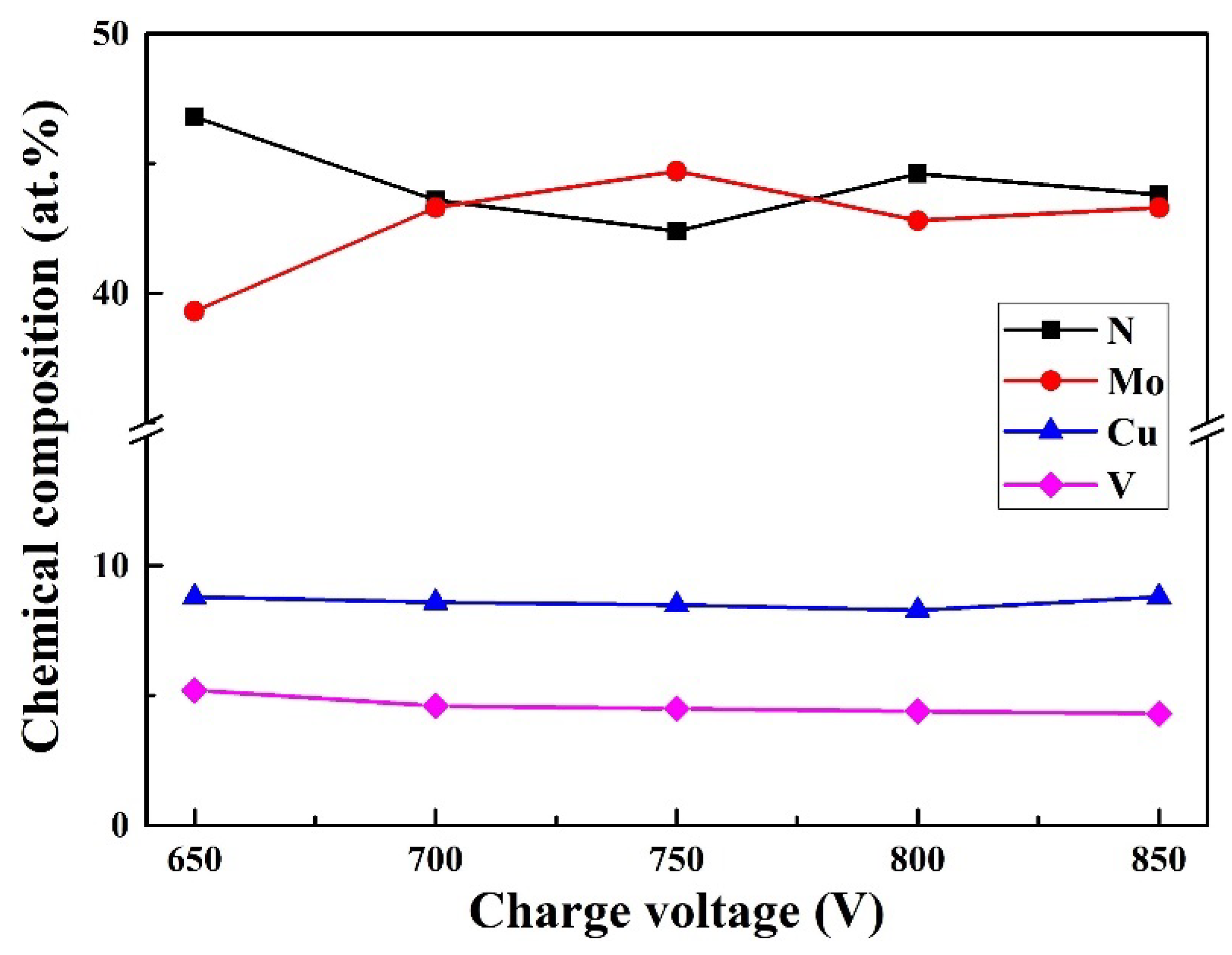
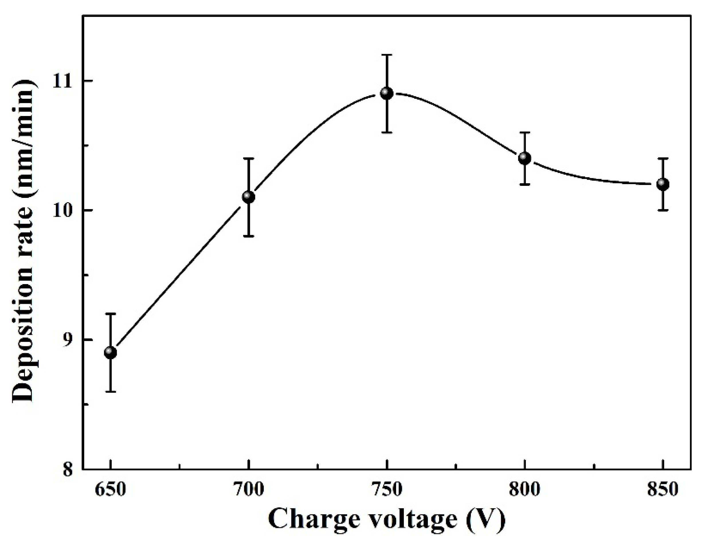
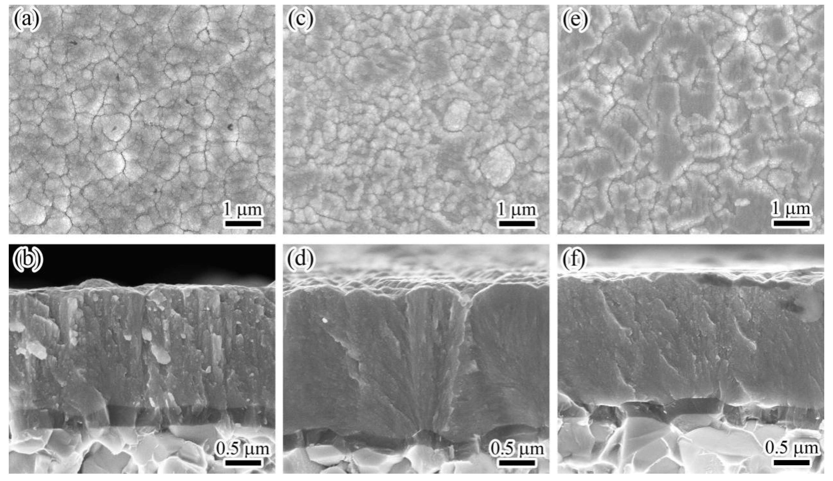
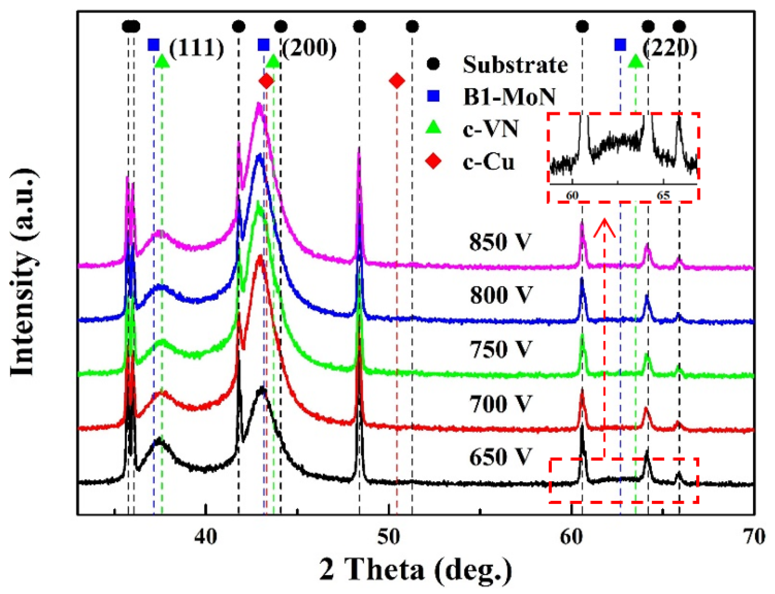
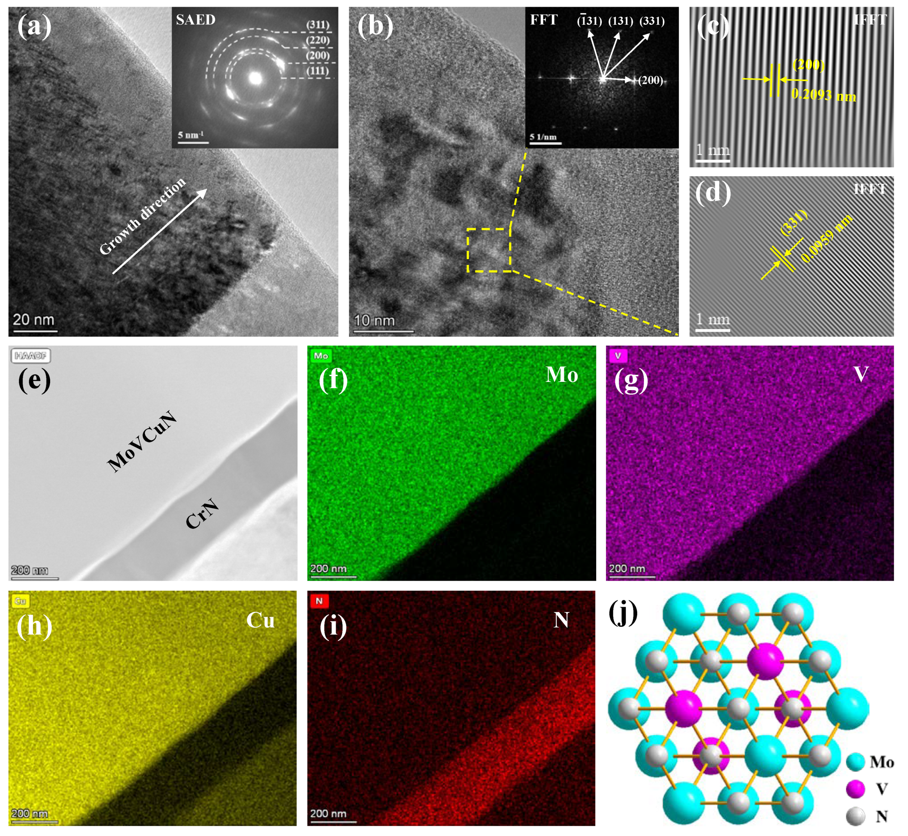
3.1. Chemical Composition and Microstructure

Figure 1 displays the chemical composition of Mo–Cu–V–N coatings as a function of charge voltage. As the charge voltage increased, the N content decreased sharply from 46.8 at. % at 650 V to 43.6 at. % at 700 V, and then remained practically constant at 42.4–44.6 at. %. The Mo content exhibited an opposite tendency, which increased from 39.3 at. % at 650 V to 43.3 at. % at 700 V, and then remained practically constant at 42.8–44.7 at. %. The Cu and V contents remained almost constant, which were varied in the small range of 8.8 at. % to 8.3 at. % and 5.2 at. % to 4.3 at. %, respectively. The N/(Mo + V) atomic ratios decreased from 1.05 at 650 V to 0.91 at 700 V, and then varied in a small range of 0.86 to 0.95 at higher charge voltages. It implied that the Mo–Cu–V–N coatings were sub-stoichiometric N at higher charge voltages above 700 V. With increasing the charge voltage, more energy was put into discharge, more charged metallic ions were accelerated flied to the substrate surface under a bias voltage, which enhanced the ion bombardment. Due to a low mass of light element, the decrease in nitrogen content can be explained by the re-sputtering effect that induced by enhanced ion bombardment at higher charge voltages. Similar phenomenon has been reported in AlCrN coatings [27] that the peak power and the degree of metal ionization increased with increasing charge voltage, which enhanced the ion bombardment and then led to the re-sputtering of N element during deposition. Figure 2 presents the deposition rate of Mo–Cu–V–N coatings as a function of charge voltage. As the charge voltage increased, the deposition rate increased from 8.9 nm/min at 650 V to 10.9 nm/min at 750 V, and then slightly decreased to 10.2 nm/min at 850 V. With increasing the charge voltage, more metallic ions were sputtered out and putted into deposition, and then led to an increase in deposition rate. However, with further increasing charge voltage, the re-sputtering effect of deposition species caused by strong ion bombardment would be enhanced, which led to a slight decrease in deposition rate at higher charge voltages above 750 V.
Figure 3 shows the SEM surface morphologies and corresponding cross-sections of Mo–Cu–V–N coatings prepared at various charge voltages. In Figure 3a,c,e, all the coating surfaces showed a typical granular structure with obvious agglomerated grains. During the coating deposition, the grains were clustered and formed a porous microstructure [12]. When charge voltage increased from 650 to 700 V, the coating surfaces changed from a loose to compact morphology. Similar results were also observed for the AlSiN and TiB2 coatings that the surface adatom energy could be increased by the enhanced ion bombardment, which promoted the migration of grain boundaries [30,31]. However, when the charge voltage was further increased, the coating surfaces became coarse with large grains agglomerated. At higher charge voltages, the extremely high-energy ion bombardment would cause the thermal effect, which would promote the grain growth during coating deposition. In Figure 3b, the coating exhibited a pronounced and coarse columnar crystal structure at 650 V. When the charge voltage increased above 700 V, the cross-sectional morphologies transformed into a dense columnar structure. Similar microstructure evolution has also been reported by Petrov et al. [32] that the adatom mobility enhanced by strong ion bombardment, which would fill the voids between grains, and disrupt the column growth, contributing to the re-nucleation and column refinement.
The XRD patterns of the coatings prepared at different charge voltages, as shown in Figure 4. At 650 V, three diffraction peaks at around 37.5°, 43.1° and 62.2° can be detected, corresponding to the (111), (200) and (220) planes with face-centered cubic structure, respectively. Based on Scherrer equation, the crystalline size of the coating calculated from (200) diffraction peak was ~5.3 nm. Because of the similar atomic radius of Mo (0.136 nm) and V (0.135 nm), a solid-solution phase of Mo–V–N could be achieved by addition of V into Mo-N lattice. When the V content was low, the V atoms in the Mo67V4N29 coating was nearly dissolved in the Mo-N phase [15]. When the V content was high, a single solid-solution phase of c-(V, Mo)N formed in the V0.57Mo0.43N0.95 coating [33]. In this study, the V content was low (4.3–5.2 at. %), a major phase of Mo–N would be formed in the Mo–Cu–V–N coatings, and the V atoms would be dissolved in the Mo-N phase. Even a high content of Cu (8.3–8.8 at. %) in the coatings, no diffraction peak of Cu phase could be detected in the XRD patterns, implying that Cu atoms existed as an amorphous phase. Similar phenomenon was observed in Mo–Cu–N coatings [12,34], the Cu atoms segregated as an amorphous phase at the grain boundary rather than in the crystalline lattices when the Cu content was below 11 at. %.
When the charge voltage increased above 700 V, the weak diffraction peak of (220) plane disappeared, and the (200) preferred orientation was further enhanced at higher charge voltages. By applying high charge voltages, the ion energy delivered to coating surface increased, contributing to an increase in adatom mobility. Thus, the adatom diffusion among grains occurred in the early and growth stage, the (200) plane with lowest surface energy would become the preferred orientation to minimize the overall energy [35]. When the charge voltage increased, the diffraction peaks shifted towards lower angles, indicating that an increase of lattice parameter. As shown in Table 2, the lattice parameters were calculated from the inter-planar spacing d200 of the preferred orientation peak. With increasing the charge voltage, the lattice parameter increased from 4.200 to 4.208 Å, which can be corresponded to the B1-MoN phase with lattice parameter ranged from 4.20 Å to 4.27 Å [12,36]. In general, the shift of diffraction peaks and the variation of lattice parameters can be caused by the high residual stress and/or interstitial solid solution in the coatings. As shown in Figure 5, all the coatings exhibited compressive residual stress due to atomic peening effect induced by ion bombardment during deposition [37]. As the charge voltage increased, the residual stress increased from 2.51 GPa at 650 V to 3.06 GPa at 700 V, and then slightly reduced to 2.87 GPa at 850 V. The initial increase in residual stress could be mainly caused by the enhanced ion bombardment at higher charge voltages [38].
The microstructure of Mo–V–Cu–N coating was further analyzed using TEM. Figure 6 displays the cross-sectional TEM images and corresponding elements mappings of the Mo–V–Cu–N coating deposited at 750 V. In Figure 6a, the coating presented a columnar structure along the growth direction in bright-field TEM image, and the corresponding SAED pattern presented a polycrystalline structure with (111), (200), (220) and (311) planes, which confirmed that the formation of c-MoVN solid-solution phase. Similar result has also been found in the Mo67V4N29 coating [15] with low V content and the V0.57Mo0.43N0.95 coating [33] with high V content. However, no diffraction ring of copper phase can be observed, it demonstrated that Cu atoms existed as an amorphous phase in Mo–V–Cu–N coatings. In Figure 6b, the high-resolution TEM (HR-TEM) image exhibited some well-crystallized grains, the corresponding FFT and IFFT patterns revealed that the diffraction rings and lattice fringes of (200) and (331) planes were belonged to the c-MoVN phase. In Figure 6e, a bi-layer structure can be seen in the HAADF image, which was consistent with the above cross-sectional SEM results. According to the STEM elements mappings, Mo, V, Cu and N elements were distributed uniformly along the cross-section, indicating that the formation of a typical nanocomposite coating. A schematic diagram of the (111) plane of B1-MoVN crystal structure, as shown in Figure 6j, the V atoms dissolved into FCC B1-MoN lattice by partial substitution of Mo, and formed solid-solution phase.

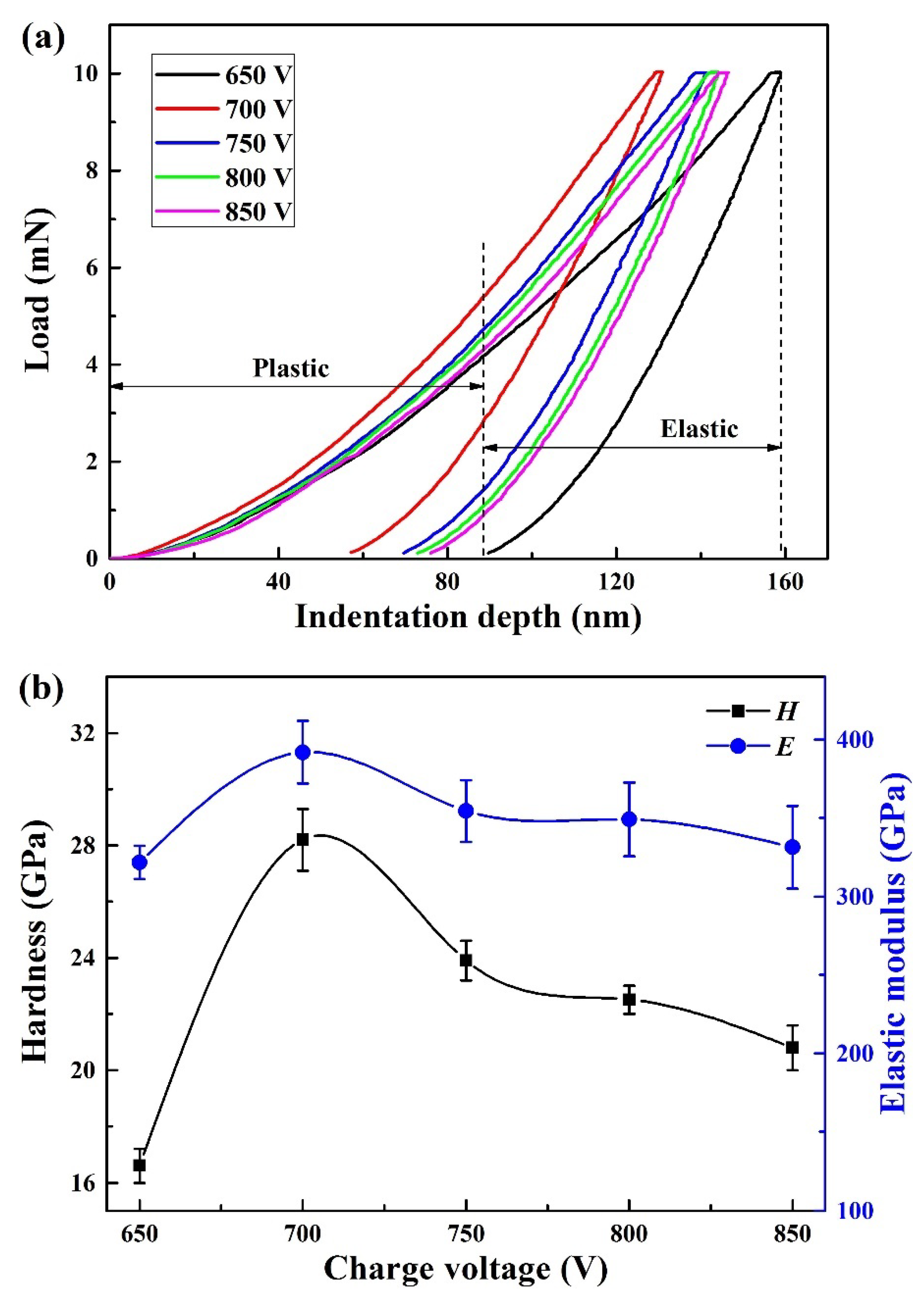
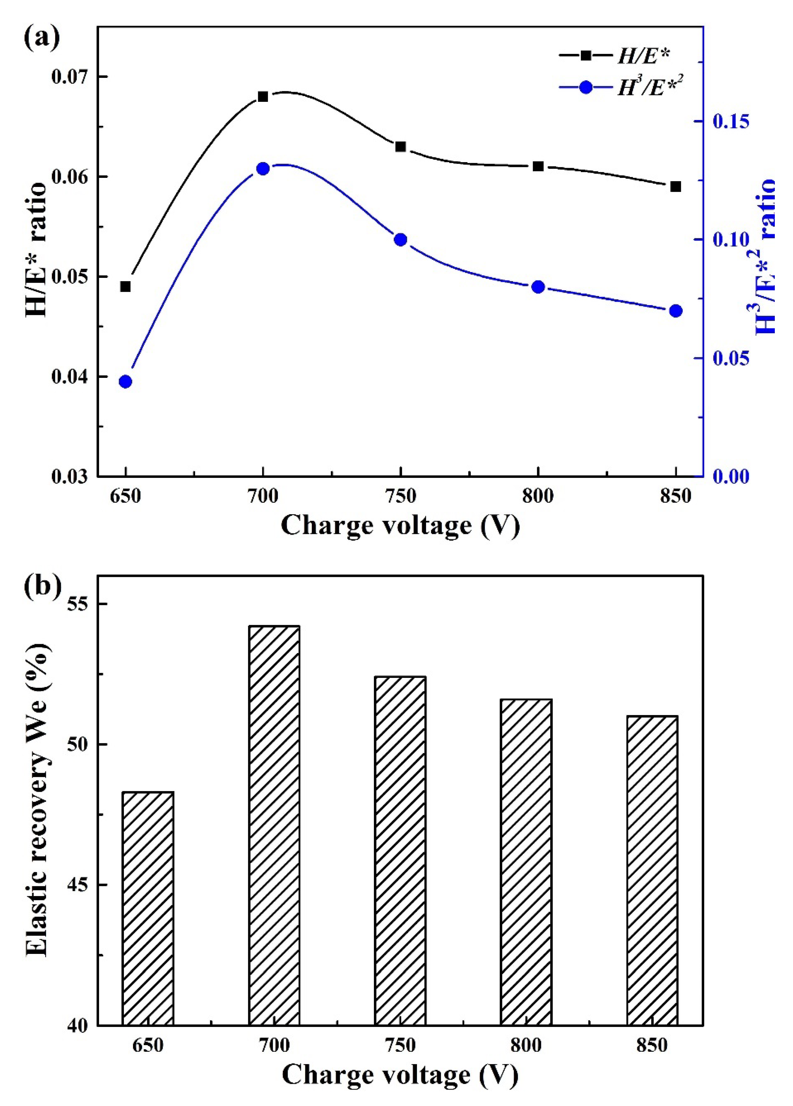
3.2. Mechanical Properties

Figure 7a displays typical indentation load–displacement curves of the coatings. It can be seen that the maximum indentation depth was below 160 nm, which was less than 10% of the total thickness of the coatings to avoid the substrate effect. Based on the above loading–unloading curves, the hardness and elastic modulus could be obtained. In Figure 7b, when the charge voltage increased, both the hardness and elastic modulus increased sharply from 16.6 and 321.6 GPa at 650 V to 28.2 and 391.9 GPa at 700 V, respectively. As the charge voltage further increased, the hardness and elastic modulus gradually reduced to 20.8 and 331.4 GPa at 850 V, respectively. Initially, the increase of hardness and elastic modulus at higher charge voltages could be attributed to the microstructure densification and an increase in residual stress [39]. However, as the charge voltage further increased, the decrease of coating hardness was mainly due to the relaxation of residual stress.
In general, the mechanical properties of hard coatings could be evaluated by the hardness (H), elastic modulus (E), H/E* ratio, H3/E*2 ratio, and elastic recovery We, etc. [40], among which the H/E* and H3/E*2 ratios can be used to predict the ability to resist elastic and plastic deformation, respectively. As shown in Figure 8a, the H/E* and H3/E*2 ratios presented a similar tendency with increasing charge voltage, both the H/E* and H3/E*2 ratios reached a maximum value of 0.068 and 0.13 at 700 V, respectively. It indicated that the best resistant against crack initiation and propagation was obtained for the coating deposited at 700 V. In addition, based on the above plastic deformation and elastic recovery curves during the loading–unloading process, the elastic recovery We can also be calculated by the ratio of recovered indentation depth to the maximum indentation depth. In Figure 8b, when charge voltage increased from 650 to 700 V, the elastic recovery We increased from 48% to 54%, and then slightly declined to 51% at 850 V.
The adhesion strength between hard coatings and substrates plays an important criterion for the coating performance. According to the adhesion strength reported by Stallard et al. [41], the adhesive failure can be classified into four modes in the scratch tests under progressive load, among which the first critical load LC1 was referred to the semi-circular cracks inside scratch track, whereas the second critical load LC2 was referred to the adhesive chipping at track edges. The critical loads LC3 and LC4 were referred to the initial failure of coatings and total failure of coatings with substrates exposed, respectively. In general, the adhesive failure mode LC2 is often used for determining the adhesion strength between coatings and substrates. Figure 9a displays the scratch track morphologies at a progressive load from 0 to 80 N. All the coatings exhibited a typical adhesive chipping at the track edges without delamination was observed, indicating that an adhesive failure mode LC2 occurred. In Figure 9b, the adhesion strength of the coatings sharply decreased from 63.9 N at 650 V to 35.7 N at 750 V, and then followed by an increase to 54.4 N at 850 V. The adhesion strength can be affected by many factors, such as the intrinsic properties of hard coating, substrate hardness, interface bonding between the coatings and substrates, etc. In this study, the variation of adhesion strength was mainly affected by the combined effect of H3/E*2 ratio and residual stress of the deposited coatings [42].

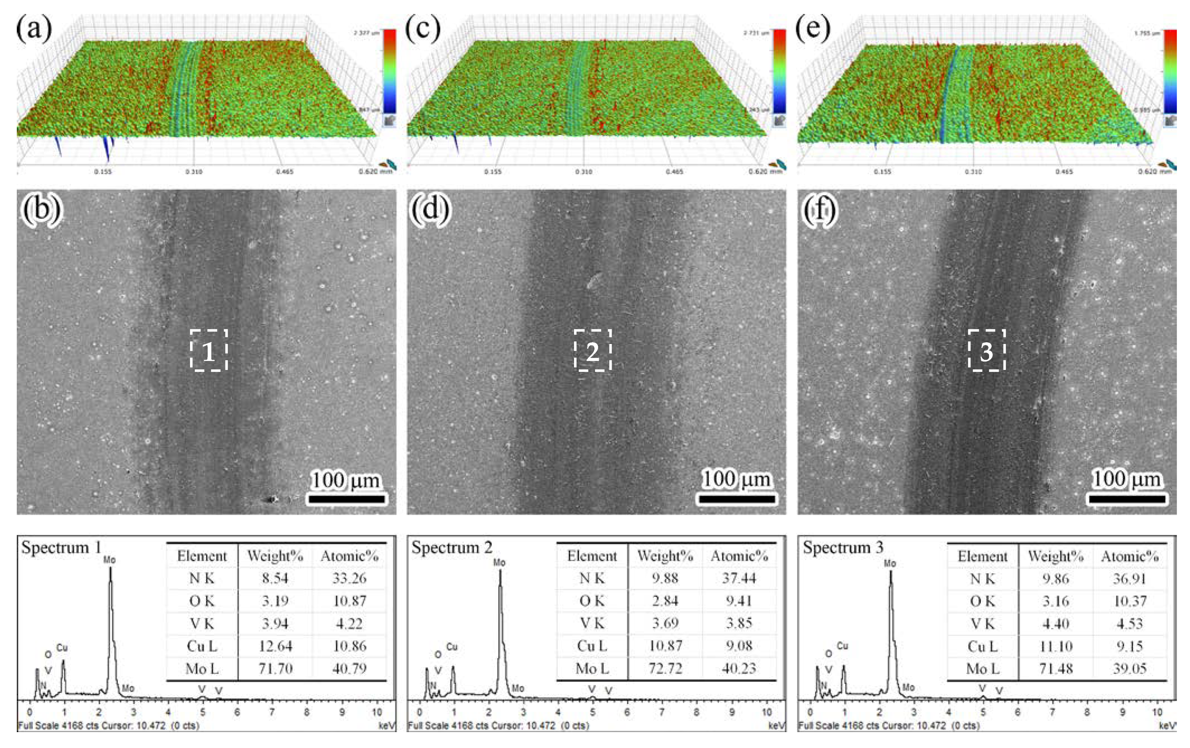
3.3. Tribological Properties

Figure 10 presents the friction coefficient and wear rate of the coatings at various charge voltages. A relatively low friction coefficient was achieved for the Mo–Cu–V–N coatings at room temperature, which varied from 0.32 to 0.35. As the charge voltage increased, the friction coefficient first slightly decreased and then rebounded at 850 V, and the wear rate exhibited a similar tendency. The wear rate decreased from 1.8 × 10⁻¹⁶ m3/N·m at 650 V to a minimum value of 6.3 × 10⁻¹⁷ m3/N·m at 750 V, and then slightly increased to 1.6 × 10⁻¹⁶ m3/N·m at 850 V. It indicated that the best tribological property was achieved at 750 V, which combined both excellent wear resistance and a low friction coefficient of 0.3. In generally, the variations of wear resistance and friction coefficient can be influenced by many factors, such as tribo-oxides formed on worn surfaces [14], the incorporation of soft metals (e.g., Ag, Cu, Ni) with low shear strength [43], and the mechanical strength of hard coatings (including the hardness and H/E* ratio) [44], etc. In this study, the best wear performance achieved at 750 V can be due to the combined effect of low friction coefficient caused by lubrication oxides and excellent wear resistance provided by enhanced mechanical strength. At 750 V, a relatively high Mo content in the coatings promoted the formation of larger fraction of MoO3 lubrication oxide on worn surface, resulting in a better wear performance [15]. Similar results were found in the Mo coatings [45], the excellent wear resistance was attributed to the high hardness and the formation of MoO3 lubrication oxide.
After sliding tests, the wear track morphologies were investigated. As shown in Figure 11a,c,e, according to the three-dimensional morphologies of wear tracks, it can be seen that some furrows formed along sliding direction, implying that mild abrasive wear occurred, which was caused by the plowing of hard particles [44]. Moreover, a much narrower and shallower wear track appeared in Figure 11c, demonstrating that an excellent wear resistance was achieved at 750 V. In Figure 11b,d,f, some wear debris were accumulated adjacent to the wear tracks. These wear debris often generated from the brittle fracture and/or asperity deformation during sliding process. The high local pressure in contact area and collide of asperity caused the friction heating, resulting in the tribo-oxidation at room temperature [46]. To identify this point, the worn surfaces were analyzed by EDS on selected zones. It revealed that the O content reached 9.4–10.9 at. %, demonstrating that a slight tribo-oxidation occurred at room temperature. Similar results have been reported in previous study [28], the formation of MoO3 and V2O5 lubrication oxides on worn surfaces contributed to low friction coefficient. Thus, the wear mechanism was dominated by mild abrasive wear and tribo-oxidation wear.

4. Conclusions

In this work, Mo–Cu–V–N coatings were designed and prepared by HIPIMS technique at various charge voltages. The mechanical and tribological properties of the coatings were greatly improved by optimization of charge voltage, which can also be applied to the optimization of other lubricating coatings. Due to the re-sputtering effect, the coatings were slightly sub-stoichiometric N at high charge voltages above 700 V. The coatings showed a solid-solution phase of B1-MoVN with (200) preferred orientation, and the preferred orientation was further enhanced at high charge voltages. Even the Cu content reached 8.3–8.8 at. %, and the Cu atoms existed as an amorphous phase in the coatings. When the charge voltage increased, more energy was put into discharge, and the enhanced ion bombardment contributed to microstructure densification and an increase in hardness. The adhesion strength reached a maximum value of 63.9 N at 650 V due to a relatively low compressive residual stress of 2.51 GPa. Due to the combined effect of low friction induced by lubrication oxides and the excellent wear resistance provided by enhanced mechanical strength, the best wear performance was achieved at 750 V, and the wear mechanism was dominated by abrasive and tribo-oxidation wear.

Author Contributions

H.M. designed the experiments and wrote manuscript; J.D. revised the manuscript; J.Z. and T.W. performed the experiments; K.H. and Z.G. analyzed the data; Q.L. and W.G. provided materials and resources. All authors have read and agreed to the published version of the manuscript.

Funding

This research was funded by National Natural Science Foundation of China (51672100), the Guangdong Basic and Applied Basic Research Foundation (2020A1515110016), International Science and Technology Cooperation Project of Guangdong Province (2019A050510049), the Professorial and Doctoral Scientific Research Foundation of Huizhou University (2020JB010), the Indigenous Innovation’s Capability Development Program of Huizhou University (HZU202005), the Key Discipline Projects of Electronic Information and Electrical Engineering of Huizhou University (2020ZD07), the Program for Innovative Research Team of Guangdong Province & Huizhou University (IRTHZU).

Institutional Review Board Statement

Not applicable.

Informed Consent Statement

Not applicable.

Data Availability Statement

Data sharing is not applicable to this article.

Conflicts of Interest

The authors declare no conflict of interest.

References

  1. Voevodin, A.A.; Muratore, C.; Aouadi, S.M. Hard coatings with high temperature adaptive lubrication and contact thermal management: Review. Surf. Coat. Technol. 2014, 257, 247–265. [Google Scholar] [CrossRef]
  2. Aouadi, S.M.; Gao, H.; Martini, A.; Scharf, T.W.; Muratore, C. Lubricious oxide coatings for extreme temperature applications: A review. Surf. Coat. Technol. 2014, 257, 266–277. [Google Scholar] [CrossRef]
  3. Torres, H.; Ripoll, M.R.; Prakash, B. Tribological behaviour of self-lubricating materials at high temperatures. Int. Mater. Rev. 2018, 63, 309–340. [Google Scholar] [CrossRef]
  4. Zhu, S.; Cheng, J.; Qiao, Z.; Yang, J. High temperature solid-lubricating materials: A review. Tribol. Int. 2019, 133, 206–223. [Google Scholar] [CrossRef]
  5. Magnéli, A. Structures of the ReO3-type with Recurrent Dislocations of Atoms: ‘Homologous Series’ of Molybdenum and Tungsten Oxides. Acta Cryst. 1953, 6, 495–500. [Google Scholar] [CrossRef] [Green Version]
  6. Franz, R.; Mitterer, C. Vanadium containing self-adaptive low-friction hard coatings for high-temperature applications: A review. Surf. Coat. Technol. 2013, 228, 1–13. [Google Scholar] [CrossRef]
  7. Zhao, H.; Guo, F.; Zhu, L.; He, J.; Yin, F. The effect of Cu addition on the crystallization behavior and tribological properties of reactive plasma sprayed TiCN-Cu coatings. Ceram. Int. 2020, 46, 8344–8351. [Google Scholar] [CrossRef]
  8. Belov, D.S.; Blinkov, I.V.; Volkhonskii, A.O. The effect of Cu and Ni on the nanostructure and properties of arc-PVD coatings based on titanium nitride. Surf. Coat. Technol. 2014, 260, 186–197. [Google Scholar] [CrossRef]
  9. Hu, J.J.; Muratore, C.; Voevodin, A.A. Silver diffusion and high-temperature lubrication mechanisms of YSZ-Ag-Mo based nanocomposite coatings. Compos. Sci. Technol. 2007, 67, 336–347. [Google Scholar] [CrossRef]
  10. Mulligan, C.P.; Papi, P.A.; Gall, D. Ag transport in CrN-Ag nanocomposite coatings. Thin Solid Films 2012, 520, 6774–6779. [Google Scholar] [CrossRef]
  11. Gulbiński, W.; Suszko, T.; Sienicki, W.; Warcholiński, B. Tribological properties of silver- and copper-doped transition metal oxide coatings. Wear 2003, 254, 129–135. [Google Scholar] [CrossRef]
  12. Shin, J.H.; Wang, Q.M.; Kim, K.H. Microstructural evolution and tribological behavior of Mo-Cu-N coatings as a function of Cu content. Mater. Chem. Phys. 2011, 130, 870–879. [Google Scholar] [CrossRef]
  13. Mei, H.; Wang, R.; Zhong, X.; Dai, W.; Wang, Q. Influence of Nitrogen Partial Pressure on Microstructure and Tribological Properties of Mo-Cu-V-N Composite Coatings with High Cu Content. Coatings 2018, 8, 24. [Google Scholar] [CrossRef] [Green Version]
  14. Mei, H.; Luo, Q.; Huang, X.; Ding, J.C.; Zhang, T.F.; Wang, Q. Influence of lubricious oxides formation on the tribological behavior of Mo-V-Cu-N coatings deposited by HIPIMS. Surf. Coat. Technol. 2019, 358, 947–957. [Google Scholar] [CrossRef] [Green Version]
  15. Wang, W.; Zheng, S.; Pu, J.; Cai, Z.; Wang, H.; Wang, L.; He, G. Microstructure, mechanical and tribological properties of Mo-V-N films by reactive magnetron sputtering. Surf. Coat. Technol. 2020, 387, 125532. [Google Scholar] [CrossRef]
  16. Sarakinos, K.; Alami, J.; Konstantinidis, S. High power pulsed magnetron sputtering: A review on scientific and engineering state of the art. Surf. Coat. Technol. 2010, 204, 1661–1684. [Google Scholar] [CrossRef]
  17. Anders, A. A review comparing cathodic arcs and high power impulse magnetron sputtering (HiPIMS). Surf. Coat. Technol. 2014, 257, 308–325. [Google Scholar] [CrossRef] [Green Version]
  18. Kouznetsov, V.; Macák, K.; Schneider, J.M.; Helmersson, U.; Petrov, I. A novel pulsed magnetron sputter technique utilizing very high target power densities. Surf. Coat. Technol. 1999, 122, 290–293. [Google Scholar] [CrossRef]
  19. Hsiao, Y.C.; Lee, J.W.; Yang, Y.C.; Lou, B.S. Effects of duty cycle and pulse frequency on the fabrication of AlCrN thin films deposited by high power impulse magnetron sputtering. Thin Solid Films 2013, 549, 281–291. [Google Scholar] [CrossRef]
  20. Chang, C.L.; Shih, S.G.; Chen, P.H.; Chen, W.C.; Ho, C.T.; Wu, W.Y. Effect of duty cycles on the deposition and characteristics of high power impulse magnetron sputtering deposited TiN thin film. Surf. Coat. Technol. 2014, 259, 232–237. [Google Scholar] [CrossRef]
  21. Nedfors, N.; Mockute, A.; Palisaitis, J.; Persson, P.O.Å.; Näslund, L.Å.; Rosen, J. Influence of pulse frequency and bias on microstructure and mechanical properties of TiB2 coatings deposited by high power impulse magnetron sputtering. Surf. Coat. Technol. 2016, 304, 203–210. [Google Scholar] [CrossRef] [Green Version]
  22. Dai, W.; Kwon, S.H.; Wang, Q.; Liu, J. Influence of frequency and C2H2 flow on growth properties of diamond-like carbon coatings with AlCrSi co-doping deposited using a reactive high power impulse magnetron sputtering. Thin Solid Films 2018, 647, 26–32. [Google Scholar] [CrossRef]
  23. Jing, F.J.; Yin, T.L.; Yukimura, K.; Sun, H.; Leng, Y.X.; Huang, N. Titanium film deposition by high-power impulse magnetron sputtering: Influence of pulse duration. Vacuum 2012, 86, 2114–2119. [Google Scholar] [CrossRef]
  24. Bagcivan, N.; Bobzin, K.; Grundmeier, G.; Wiesing, M.; Ozcan, O.; Kunze, C.; Brugnara, R.H. Influence of HPPMS pulse length and inert gas mixture on the properties of (Cr,Al)N coatings. Thin Solid Films 2013, 549, 192–198. [Google Scholar] [CrossRef]
  25. Anders, A.; Andersson, J.; Ehiasarian, A. High power impulse magnetron sputtering: Current-voltage-time characteristics indicate the onset of sustained self-sputtering. J. Appl. Phys. 2007, 102, 113303. [Google Scholar] [CrossRef] [Green Version]
  26. Depla, D.; Mahieu, S.; Gryse, R.D. Magnetron sputter deposition: Linking discharge voltage with target properties. Thin Solid Films 2009, 517, 2825–2839. [Google Scholar] [CrossRef]
  27. Zheng, J.; Zhou, H.; Gui, B.; Luo, Q.; Li, H.; Wang, Q. Influence of Power Pulse Parameters on the Microstructure and Properties of the Alcrn Coatings by a Modulated Pulsed Power Magnetron Sputtering. Coatings 2017, 7, 216. [Google Scholar] [CrossRef] [Green Version]
  28. Mei, H.; Zhao, S.; Wu, Z.; Dai, W.; Wang, Q. Effect of nitrogen partial pressure on microstructure and mechanical properties of Mo-Cu-V-N composite coatings deposited by HIPIMS. Surf. Coat. Technol. 2017, 329, 68–76. [Google Scholar] [CrossRef]
  29. Stoney, G.G. The tension of metallic films deposited by electrolysis. Proc. R. Soc. Lond. A Math. Phys. Sci. 1909, 82, 172–175. [Google Scholar]
  30. Ding, J.C.; Wang, Q.M.; Liu, Z.R.; Jeong, S.; Zhang, T.F.; Kim, K.H. Influence of bias voltage on the microstructure, mechanical and corrosion properties of AlSiN films deposited by HiPIMS technique. J. Alloys Compd. 2019, 772, 112–121. [Google Scholar] [CrossRef]
  31. Zhang, T.F.; Gan, B.; Park, S.; Wang, Q.M.; Kim, K.H. Influence of negative bias voltage and deposition temperature on microstructure and properties of superhard TiB2 coatings deposited by high power impulse magnetron sputtering. Surf. Coat. Technol. 2014, 253, 115–122. [Google Scholar] [CrossRef]
  32. Petrov, I.; Barna, P.B.; Hultman, L.; Greene, J.E. Microstructural evolution during film growth. J. Vac. Sci. Technol. A 2003, 21, S117–S128. [Google Scholar] [CrossRef]
  33. Mikula, M.; Uzon, S.; Hudec, T.; Grančič, B.; Truchlý, M.; Roch, T.; Švec, P., Jr.; Satrapinskyy, L.; Čaplovičová, M.; Greczynski, G.; et al. Thermally induced structural evolution and age-hardening of polycrystalline V1−xMoxN (x ≈ 0.4) thin films. Surf. Coat. Technol. 2021, 405, 126723. [Google Scholar] [CrossRef]
  34. Kim, J.N.; Park, S.; Kim, T.; Lee, J.J. Structure and mechanical properties of Mo-N/Cu films produced by inductively coupled plasma reactive sputtering. Thin Solid Films 2011, 519, 6876–6880. [Google Scholar] [CrossRef]
  35. Kajikawa, Y.; Noda, S.; Komiyama, H. Comprehensive perspective on the mechanism of preferred orientation in reactive-sputter-deposited nitrides. J. Vac. Sci. Technol. A 2003, 21, 1943–1954. [Google Scholar] [CrossRef]
  36. Ihara, H.; Kimura, Y.; Senzaki, K.; Kezuka, H.; Hirabayashi, M. Electronic structures of B1 MoN, fcc Mo2N, and hexagonal MoN. Phys. Rev. B 1985, 31, 3177–3178. [Google Scholar] [CrossRef]
  37. Windischmann, H. Intrinsic stress in sputter-deposited thin-films. Crit. Rev. Solid State 1992, 17, 547–596. [Google Scholar] [CrossRef]
  38. Ljungcrantz, H.; Hultman, L.; Sundgren, J.-E.; Karlsson, L. Ion induced stress generation in arc-evaporated TiN films. J. Appl. Phys. 1995, 78, 832–837. [Google Scholar] [CrossRef]
  39. Wan, X.S.; Zhao, S.S.; Yang, Y.; Gong, J.; Sun, C. Effects of nitrogen pressure and pulse bias voltage on the properties of Cr-N coatings deposited by arc ion plating. Surf. Coat. Technol. 2010, 204, 1800–1810. [Google Scholar] [CrossRef]
  40. Musil, J.; Kunc, F.; Zeman, H.; Poláková, H. Relationships between hardness, Young’s modulus and elastic recovery in hard nanocomposite coatings. Surf. Coat. Technol. 2002, 154, 304–313. [Google Scholar] [CrossRef]
  41. Stallard, J.; Poulat, S.; Teer, D.G. The study of the adhesion of a TiN coating on steel and titanium alloy substrates using a multi-mode scratch tester. Tribol. Int. 2006, 39, 159–166. [Google Scholar] [CrossRef]
  42. Mei, H.; Geng, D.; Wang, R.; Cheng, L.; Ding, J.C.; Luo, Q.; Zhang, T.F.; Wang, Q. Effect of Cu doping on the microstructure and mechanical properties of AlTiVN-Cu nanocomposite coatings. Surf. Coat. Technol. 2020, 402, 126490. [Google Scholar] [CrossRef]
  43. Wang, W.; Pu, J.; Cai, Z.; Zheng, S.; Wei, Y. Insights into friction properties and mechanism of self-lubricating MoVN-Ag films at high temperature. Vacuum 2020, 176, 109332. [Google Scholar] [CrossRef]
  44. Yang, K.; Xian, G.; Zhao, H.; Fan, H.; Wang, J.; Wang, H.; Du, H. Effect of Mo content on the structure and mechanical properties of TiAlMoN films deposited on WC-Co cemented carbide substrate by magnetron sputtering. Int. J. Refract. Metals Hard Mater. 2015, 52, 29–35. [Google Scholar] [CrossRef]
  45. Deng, X.; Zhang, G.; Wang, T.; Ren, S.; Cao, Q.; Bai, Z.; Liu, Z. Microstructure and wear resistance of Mo coating deposited by plasma transferred arc process. Mater. Charact. 2017, 131, 517–525. [Google Scholar] [CrossRef]
  46. Holmberg, K.; Ronkainen, H.; Matthews, A. Tribology of thin films. Ceram. Int. 2000, 26, 787–795. [Google Scholar] [CrossRef]
Figure 1. Chemical composition of Mo–Cu–V–N coatings as a function of charge voltage.
Coatings 11 01565 g001
Figure 2. Deposition rate of Mo–Cu–V–N coatings as a function of charge voltage.
Coatings 11 01565 g002
Figure 3. Surface and cross-sectional micrographs of the coatings at various charge voltages: (a,b) 650 V, (c,d) 700 V, and (e,f) 850 V.
Coatings 11 01565 g003
Figure 4. XRD patterns of Mo–Cu–V–N coatings at various charge voltages.
Coatings 11 01565 g004
Figure 5. Residual stress of Mo–Cu–V–N coatings at various charge voltages.
Coatings 11 01565 g005
Figure 6. Cross-sectional TEM images of the Mo–Cu–V–N coating prepared at 750 V: (a) TEM image and corresponding SAED pattern, (bd) HRTEM image with corresponding FFT/IFFT patterns, (ei) HAADF image and STEM elements mappings, (j) schematic diagram of (111) plane of B1-MoVN crystal structure.
Coatings 11 01565 g006
Figure 7. Typical indentation load–displacement curves (a), hardness and elastic modulus (b) of the coatings at various charge voltages.
Coatings 11 01565 g007
Figure 8. H/E* and H3/E*2 ratio (a), elastic recovery We (b) of Mo–Cu–V–N coatings at various charge voltages.
Coatings 11 01565 g008
Figure 9. Scratch tracks (a) and adhesion strength (b) of the coatings at various charge voltages.
Coatings 11 01565 g009
Figure 10. Friction coefficient and wear rate of Mo–Cu–V–N coatings as a function of charge voltage.
Coatings 11 01565 g010
Figure 11. Three-dimensional morphologies, surface micrographs, and EDS results of the selected wear tracks: (a,b) 650 V, (c,d) 750 V, and (e,f) 850 V.
Coatings 11 01565 g011
Table 1. Deposition parameters of Mo–Cu–V–N coatings.
ParametersValues
Base pressure (Pa)5.0 × 10⁻³
Working pressure (Pa)0.7
N2/Ar flow rate (sccm)10/35
Substrate temperature (°C)200
Substrate bias voltage (V)−100
Target to substrate distance (mm)120
Target power (kW)1.0
Duty cycle3%
Pulse width (μs)150
Frequency (Hz)200
Charge voltage (V)650, 700, 750, 800, 850
Deposition time (min)180
Table 2. Lattice parameters of Mo–Cu–V–N coatings at various charge voltages.
PhaseLattice Parameter a0 (Å)
B1-MoVN650 V700 V750 V800 V850 V
4.2004.2064.2084.2084.208
Publisher’s Note: MDPI stays neutral with regard to jurisdictional claims in published maps and institutional affiliations.

