Article

Carrier Modulation in Bi2Te3-Based Alloys via Interfacial Doping with Atomic Layer Deposition

1
Center for Electronic Materials, Korea Institute of Science and Technology, Seoul 02792, Korea
2
Department of Materials Science and Engineering, Yonsei University, Seoul 03722, Korea
3
Department of Materials Science and Chemical Engineering, Hanyang University, Ansan 15588, Korea
4
Yonsei-KIST Convergence Research Institute, Seoul 02792, Korea
5
Division of Nano & Information Technology, KIST School, Korea University of Science and Technology, Seoul 02792, Korea
*
Authors to whom correspondence should be addressed.
Coatings 2020, 10(6), 572; https://doi.org/10.3390/coatings10060572
Submission received: 29 May 2020 / Revised: 15 June 2020 / Accepted: 16 June 2020 / Published: 18 June 2020
(This article belongs to the Special Issue Thin Films by Atomic Layer Deposition: Properties and Applications)

Abstract

:
The carrier concentration in Bi2Te3-based alloys is a decisive factor in determining their thermoelectric performance. Herein, we propose a novel approach to modulate the carrier concentration via the encapsulation of the alloy precursor powders. Atomic layer deposition (ALD) of ZnO and SnO2 was performed over the Bi2Te2.7Se0.3 powders. After spark plasma sintering at 500 °C for 20 min, the carrier concentration in the ZnO-coated samples decreased, while the carrier concentration in the SnO2-coated samples increased. This trend was more pronounced as the number of ALD cycles increased. This was attributed to the intermixing of the metal ions at the interface. Zn2+ substituted for Bi3+ at the interface acted as an acceptor, while Sn4+ substituted for Bi3+ acted as a donor. This indicates that the carrier concentration can be adjusted depending on the materials deposited with ALD. The use of fine powders changes the carrier concentration more strongly, because the quantity of material deposited increases with the effective surface area. Therefore, the proposed approach would provide opportunities to precisely optimize the carrier concentration for high thermoelectric performance.

1. Introduction

Bi2Te3-based alloys have received a great deal of attention for thermoelectric applications operating at room temperature, because Bi2Te3-based alloys have superior thermoelectric performance near room temperature for both n- and p-type conduction [1,2,3,4,5]. It includes two typical applications such as solid-state coolers and power generation. Since the thermoelectric cooler has no moving parts, it is favorable for cooling systems requiring low noise and non-vibration [6], Electricity can also be generated by the thermoelectric Bi2Te3-based alloys from areas where there is a temperature difference on each side. Human bodies can be a good energy source to scavenge the waste heat near room temperature. Therefore, much efforts have been dedicated to the development of wearable energy harvesting using the thermoelectric Bi2Te3-based alloys [7,8,9,10]. The thermoelectric performance of the materials is defined by the figure-of-merit, zT = S2σT/κ, where S is the Seebeck coefficient, σ is the electrical conductivity, T is the absolute temperature, and κ is the thermal conductivity. The parameters S, σ, and κ are each a function of the carrier concentration, and these parameters are strongly coupled with each other. Therefore, carrier concentration is regarded as one of the critical parameters for optimizing the thermoelectric performance of a material.
The most common strategy for tuning the carrier concentration of Bi2Te3-based alloys is to uniformly incorporate impurity atoms with different valence states. Single elements have been commonly used as doping materials for this purpose. Some elements including Br [11], I [12], Ge [13,14] were reported as a donor, and the other elements such as Sn [15,16], Pb [17,18], Sb [19] were proposed as an acceptor in Bi2Te3-based alloys. However, these elements are often distributed non-uniformly in the matrix, and even partially activated as a dopant. Therefore, the carrier concentration is often not proportional to the amount of the dopants. In addition, some elements show amphoteric behavior in Bi2Te3-based alloys. In cases of the elements such as Ag and Cu, some groups reported Ag [20,21] and Cu [22,23,24,25] as a donor, while the others reported the p-type behavior of Ag [26] and Cu [27,28,29]. This amphoteric behavior results from the existence of various types of lattice defects [30], which are significantly dependent on the process conditions. Thus, this could be implicated in the large scattering for the reported carrier concentrations.
Compound dopants [31,32,33,34], such as CuBr and SbI3, have also been used as doping materials. However, these halides can be partially decomposed in the synthesis process of thermoelectric Bi2Te3-based legs [35]. This makes it difficult to have precise control of the carrier concentration. Indeed, it was reported that the carrier concentration for Bi2Te3-based alloys was required to be modulated within a very narrow range of 2–6 × 10¹⁹/cm3 for optimizing the thermoelectric performance [36]. Therefore, it is imperative to develop a new doping method that can precisely control the carrier concentration in such a narrow range.
Recently, we reported that the carrier concentration of ZnO/Bi2Te3 heterostructures changed with the intermixing of Zn2+ and Bi3+ ions at the interface [37]. This suggests that the carrier concentration can be modulated by coating Bi2Te3-based grains with a thin hetero-material layer. In this study, we demonstrate carrier modulation in Bi2Te3-based alloys via interfacial doping with atomic layer deposition (ALD). We further demonstrate that the carrier concentration of the alloy can be increased or decreased, depending on the valence states of the metal ions in the ALD-grown-material.

2. Materials and Methods

Bi2Te2.7Se0.3 was prepared by melting the constituent materials in a rocking furnace at 800 °C for 6 h and subsequent quenching. The Bi2Te2.7Se0.3 chunks were ball-milled with zirconia balls for 24 h under an Ar atmosphere, to produce a fine powder. ZnO and SnO2 thin films were grown over the Bi2Te2.7Se0.3 powders by ALD in a home-built vibrated chamber. Diethylzinc (DEZ) and Tetrakis(dimethylamino)tin (TDMASn) were used as the Zn and Sn sources, respectively. H2O was employed as the oxygen source for the growth of ZnO and SnO2. The film growth was performed at room temperature for ZnO and 65 °C for SnO2, respectively. An ALD cycle consists of metal precursor injection-purge-H2O injection-purge. The amount of the ALD-grown film was controlled by changing the number of ALD cycles. The detailed conditions for the ALD process are reported elsewhere [38,39]. The metal-oxide-coated Bi2Te2.7Se0.3 powders were sintered by spark plasma sintering (SPS) (Elteck Korea Co., Anyang, Korea) at 500 °C for 20 min, under an applied pressure of 40 MPa.
The microstructure of the SPS Bi2Te2.7Se0.3 material was examined with scanning transmission electron microscopy (STEM) (FEI, Hillsboro, Ore., USA). X-ray photoelectron spectroscopy (XPS) (ULVAC-PHI, Chigasaki, Japan) was employed to examine the chemical states of the coated materials. The Seebeck coefficient was measured using a standard four-probe method at room temperature. The carrier concentration and mobility were measured by the Hall measurement, using van der Pauw geometry.

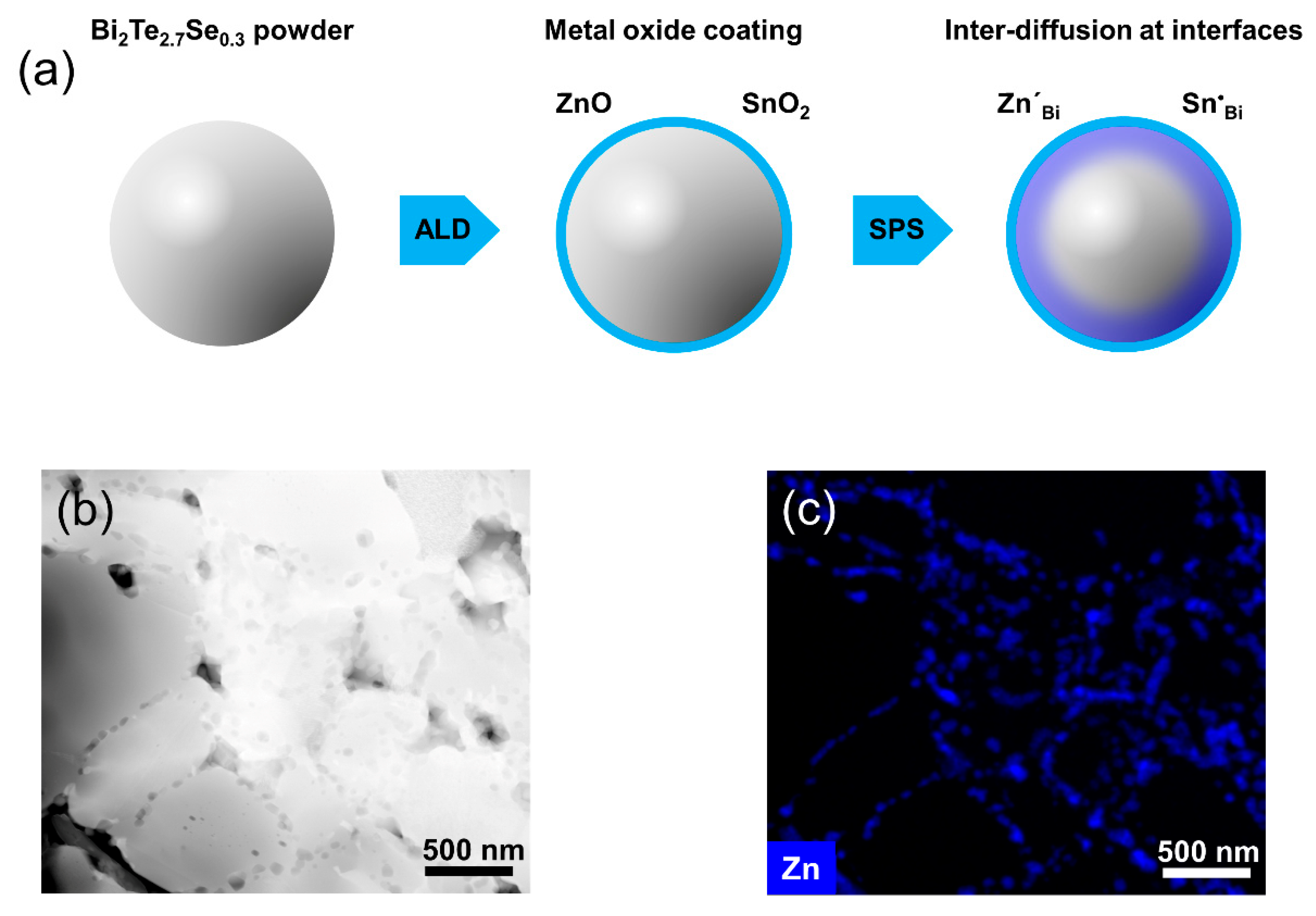
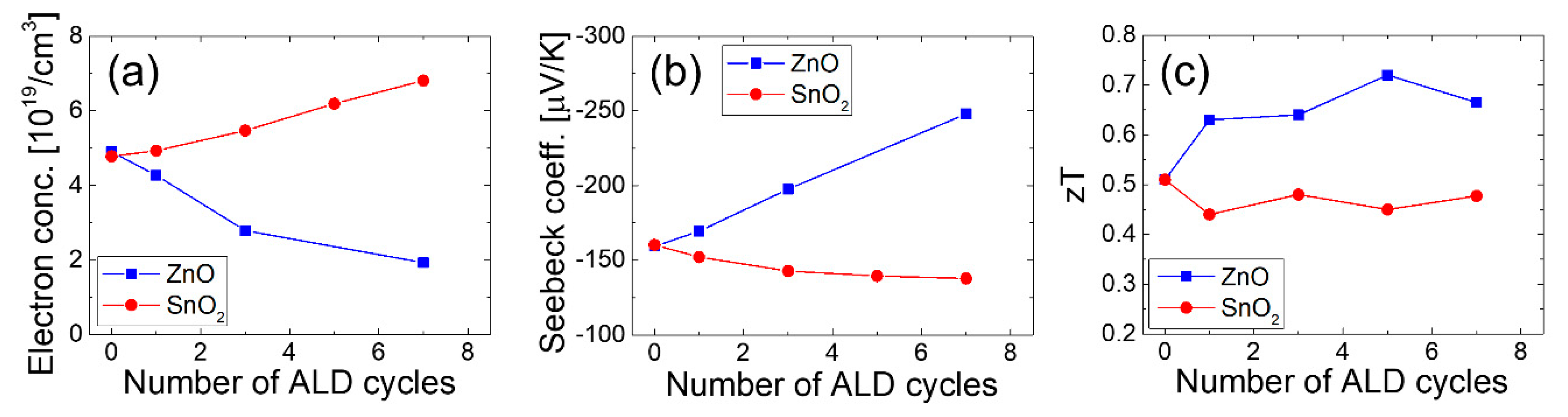
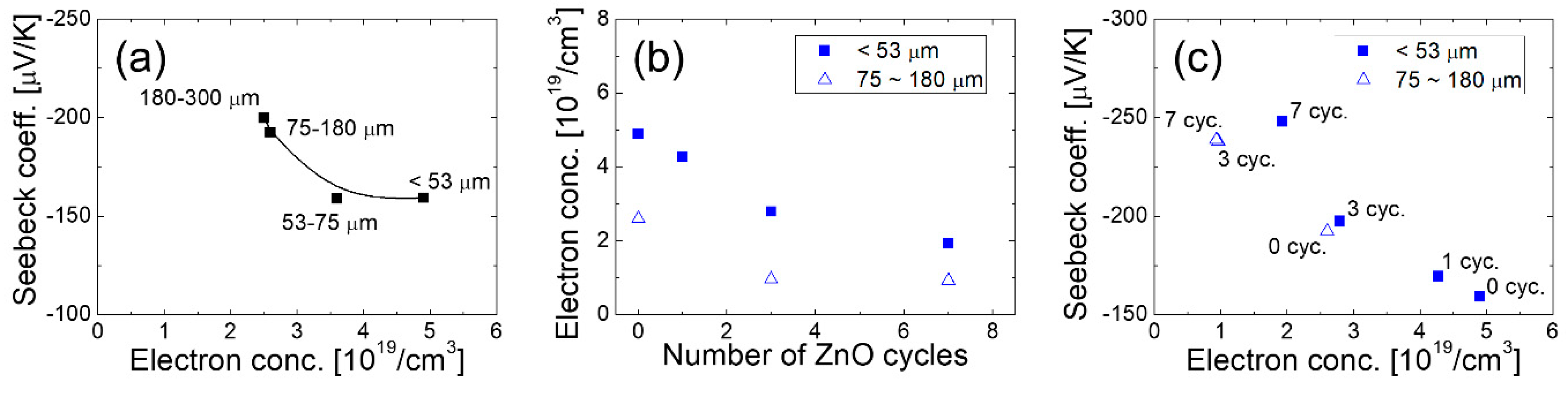
3. Results and Discussion

Figure 1a illustrates the strategy used to modulate the carrier concentration via interfacial doping. For the interfacial doping, a very thin oxide layer was grown over n-type Bi2Te2.7Se0.3 powders. ALD, which is based on a self-limiting mechanism, was employed for the conformal growth of the metal oxide on the powders. The metal ions in the ALD-grown layer could intermix with the Bi2Te3-based alloys near the interface during the SPS process, and these metal ions were substituted for the Bi3+ ions near the interface. In order to optimize the carrier concentration, the ALD-grown oxide layer should be able to act as either a donor or an acceptor for the Bi2Te3-based alloys. Hence, the selection of a proper growth material is a critical factor in modulating the carrier concentration. Here, we selected ZnO and SnO2 as the materials used to decrease and increase the carrier concentration, respectively. The cations in both materials had valence states different from the Bi3+ ions in the Bi2Te3-based alloys. It was expected that the ALD of ZnO and SnO2 would decrease or increases the electron concentration in the n-type Bi2Te2.7Se0.3, by the substitution of Bi3+ with Zn2+ or Sn4+, respectively.
After undergoing the SPS process, the microstructure of the ALD-coated Bi2Te2.7Se0.3 was observed. Figure 1b shows a high-angle annular dark-field (HAADF) STEM image of the SPS pellet of ZnO-coated Bi2Te2.7Se0.3. The Zn element map corresponding to the area observed in Figure 1b is presented in Figure 1c. These TEM results reveal that the Bi2Te2.7Se0.3 grains were encapsulated by a very thin ZnO layer, even after SPS at a temperature of 500 °C. The heterogeneous interfaces were well-developed through the ALD technique. The appearance of the heterogeneous interfaces was attributed to the low solubility of the oxides in Bi2Te2.7Se0.3 and the large differences in the melting points between the oxides (ZnO: 1975 °C and SnO2: 1630 °C) and Bi2Te2.7Te0.3 (approximately 606 °C). These heterogeneous interfaces were also observed in the SPS pellets of p-type Bi0.4Sb1.6Te3 with an ALD-grown ZnO layer [38]. This suggests that a strategy based on this ALD technique is generally effective on Bi2Te3-based alloys, irrespective of the conduction type. The size of the Bi2Te2.7Se0.3 grains was found to be small, generally below 1 µm. Given that the grains of Bi2Te3-based alloys generally grow to a larger size after SPS at high temperatures, such as 500 °C [40], this suggests that the ALD of a thin oxide layer effectively suppressed the grain growth during the sintering process. Indeed, it has been previously reported that an extremely low κ value was obtained in the ALD-ZnO-coated Bi0.4Sb1.6Te3, due to the formation of fine grains [38].
Figure 2a,b show the XPS spectra of (a) Zn 2p and (b) Sn 3d core levels in the SPS pellets of ZnO-coated and SnO2-coated Bi2Te2.7Se0.3, respectively. A single Zn 2p3/2 peak was observed at 1021.5 eV, corresponding to the Zn2+ valence state. The Sn 3d XPS spectra showed a single peak positioned at 486.5 eV, which corresponded to Sn4+. No peaks corresponding to the other valence states were observed in either spectra. This means that the cations in the oxide layers preserved their own valence states, even after the high-temperature sintering process. This also suggests the possibility for these cations to act as an acceptor or a donor if the cations were substituted for Bi ions at the heterointerfaces.
The electrical properties of the SPS ALD-coated Bi2Te2.7Se0.3 pellets were quantified, to verify the doping effects of the coating materials. Figure 3a shows the variation in the electron concentration of the ZnO- and SnO2-coated Bi2Te2.7Se0.3 pellets as a function of the number of ALD cycles. Interestingly, the two oxides, which are n-type semiconductors, exhibited opposite effects on the electrical properties of Bi2Te2.7Se0.3. As the number of ALD cycles increased, the electron concentration in the ZnO-coated Bi2Te2.7Se0.3 decreased, while the electron concentration in the SnO2-coated Bi2Te2,7Se0.3 increased. This indicates that the ALD-grown ZnO and SnO2 layers could act as an acceptor and a donor, respectively, in Bi2Te2,7Se0.3 through substitution for the Bi ions, which is consistent with the expectation proposed in Figure 1a. It was also found that the change in the electron concentration per ALD cycle was larger for the ZnO-coated Bi2Te2,7Se0.3 than for the SnO2-coated Bi2Te2,7Se0.3. The difference resulted from the difference in the growth-per-cycle of the ALD processes of ZnO and SnO2. Figure 4 shows the variation in the film thickness of ZnO and SnO2 grown on Si substrate, as a function of the number of ALD cycles. The growth per ALD cycle of the materials is estimated from the linear fit of the graph. The growth per cycle of ZnO is 0.65 nm/cycle and the growth per ALD cycle of SnO2 is 0.23 nm/cycle.
Given that the value of S is closely related to the electron concentration, it was necessary to examine the variation in the S value in terms of the number of ALD cycles. Figure 3b shows the variation in the S value of the ZnO- and SnO2-coated Bi2Te2.7Se0.3 pellets, as a function of the number of ALD cycles. As the number of the ALD cycles increased from 0 to 7 cycles, the S value of ZnO-coated Bi2Te2.7Se0.3 grew from −160 to −250 µV/K, while the S value of SnO2-coated Bi2Te2.7Se0.3 dropped to −138 µV/K. Considering the fact that the S value is inversely proportional to the electron concentration, this result was consistent with the variation in the electron concentration shown in Figure 3a. The zT value of the SPS pellets was also influenced by the ZnO and SnO2 ALD coatings, as shown in Figure 3c. The zT value of uncoated Bi2Te2.7Se0.3 was approximately 0.5. The zT value increased to 0.7 after the ALD of ZnO, because the electron concentration was moderated by the ALD coating. On the other hand, the ALD of SnO2 further increased the electron concentration, resulting in the deterioration of the zT value down to 0.45. Therefore, coating Bi2Te2.7Se0.3 with a very thin oxide layer through ALD could be a promising way to enhance the thermoelectric properties via carrier modulation.
The carrier modulation was closely related to the amount of oxide grown over the particles. That is the reason why the electron concentration in Figure 3a changed with the number of ALD cycles. In addition to cycle variation, the quantity of the grown oxide could change with the effective surface area of the Bi2Te2.7Se0.3 powders. This suggests that the size of the powders was another factor that affected the carrier modulation. First, we examined the electrical properties of the uncoated Bi2Te2.7Se0.3 pellets in terms of the powder size (Figure 5a). Despite the powders having the same composition and identical SPS conditions, the electron concentration decreased and the S value increased as the size of the powder increased. The increase in the electron concentration as the powders became finer was due to the increase in number of grain boundaries. A previous study has reported that grain boundaries in Bi2Te3 acted as an electron source [41].
For comparison, we examined the electrical properties of ZnO-coated Bi2Te2.7Se0.3 with two different powder sizes of <53 µm and 75–180 µm. We chose ZnO as the ALD-grown material, because the ALD of ZnO improved the thermoelectric performance of n-type Bi2Te2.7Se0.3, as previously shown in Figure 3c. Figure 5b shows the variation in the electron concentration of the ZnO-coated Bi2Te2.7Se0.3, with different powder sizes, as a function of the number of ZnO ALD cycles. Although the electron concentration decreased with increasing the number of ZnO ALD cycles for both powder sizes, the electron concentration in the SPS pellet made from a powder with particle sizes of <53 µm decreased more abruptly than the electron concentration in the SPS pellet made from powder with particle sizes of 75–180 µm. The S values increased as the number of ZnO ALD cycles increased as well, due to the decrease in the electron concentration, as shown in Figure 5c. This indicates that the carrier concentration can be exquisitely tuned by the controlling in number of ALD cycles and the powder size.

4. Conclusions

We proposed a novel strategy to modulate the carrier concentration in Bi2Te3-based thermoelectric alloys via an ALD technique. The ALD of oxide layers grown over Bi2Te2.7Se0.3 powders changed the carrier concentration by doping through intermixing metal ions at the interfaces. The electron concentration was found to be modulated depending on the valence state of the cations in the oxide layer; e.g., the ALD of ZnO with Zn2+ decreased the electron concentration while the ALD of SnO2 with Sn4+ increased the electron concentration. Consequently, the carrier concentration can be precisely controlled, even in a very narrow range of 2–6 × 10¹⁹/cm3 for the optimized performance. It was also shown that the carrier concentration could also vary with powder size. This ALD-based approach provides the ability to optimize the thermoelectric performance of Bi2Te3-based alloys via explicit modulation of the carrier concentration.

Author Contributions

Conceptualization, S.-S.L., J.-S.K., and S.K.K; methodology, S.-S.L., K.-C.K. and S.L.; writing—original draft preparation, S.K.K.; writing—review and editing, S.-S.L., H.-H.P., J.-S.K. and S.K.K.; supervision, S.-H.B., J.-S.K. and S.K.K.; project administration, J.-S.K. All authors have read and agreed to the published version of the manuscript.

Funding

We would like to acknowledge the financial support from the R&D Convergence Program of NST (National Research Council of Science and Technology) of Republic of Korea.

Conflicts of Interest

The authors declare no conflict of interest.

References

  1. Venkatasubramanian, R.; Siivola, E.; Colpitts, T.; O’Quinn, B. Thin-film thermoelectric devices with high room-temperature figures of merit. Nature 2001, 413, 597–602. [Google Scholar] [CrossRef] [PubMed]
  2. Kim, S.I.; Lee, K.H.; Mun, H.A.; Kim, H.S.; Hwang, S.W.; Roh, J.W.; Yang, D.J.; Shin, W.H.; Li, X.S.; Lee, Y.H.; et al. Dense dislocation arrays embedded in grain boundaries for high-performance bulk thermoelectrics. Science 2015, 348, 109–114. [Google Scholar] [CrossRef] [PubMed] [Green Version]
  3. Chowdhury, I.; Prasher, R.; Lofgreen, K.; Chrysler, G.; Narasimhan, S.; Mahajan, R.; Koester, D.; Alley, R.; Venkatasubramanian, R. On-chip cooling by superlattice-based thin-film thermoelectrics. Nat. Nanotechnol. 2009, 4, 235–238. [Google Scholar] [CrossRef]
  4. Yan, X.; Poudel, B.; Ma, Y.; Liu, W.S.; Joshi, G.; Wang, H.; Lan, Y.; Wang, D.; Chen, G.; Ren, Z.F. Experimental studies on anisotropic thermoelectric properties and structures of n-type Bi2Te2.7Se0.3. Nano. Lett. 2010, 10, 3373–3378. [Google Scholar] [CrossRef]
  5. DiSalvo, F.J. Thermoelectric cooling and power generation. Science 1999, 285, 703–706. [Google Scholar] [CrossRef]
  6. MohanKumar, P.; Babu, V.J.; Subramanian, A.; Bandla, A.; Thakor, N.; Ramakrishna, S.; Wei, H. Thermoelectric materials—strategies for improving device performance and its medical applications. Science 2019, 1, 37. [Google Scholar] [CrossRef] [Green Version]
  7. Leonov, V.; Vullers, R.J.M. Wearable electronics self-powered by using human body heat: The state of the art and the perspective. J. Renew. Sustain. Energy 2009, 1, 062701. [Google Scholar] [CrossRef]
  8. Hyland, M.; Hunter, H.; Liu, J.; Veety, E.; Vashaee, D. Wearable thermoelectric generators for human body heat harvesting. Appl. Energy 2016, 182, 518–524. [Google Scholar] [CrossRef] [Green Version]
  9. Kim, C.S.; Yang, H.M.; Lee, J.; Lee, G.S.; Choi, H.; Kim, Y.J.; Lim, S.H.; Cho, S.H.; Cho, B.J. Self-powered wearable electrocardiography using a wearable thermoelectric power generator. ACS Energy Lett. 2018, 3, 501–507. [Google Scholar] [CrossRef]
  10. Lee, Y.G.; Kim, J.; Kang, M.-S.; Baek, S.-H.; Kim, S.K.; Lee, S.-M.; Lee, J.; Hyun, D.-B.; Ju, B.-K.; Moon, S.E.; et al. Design and experimental investigation of thermoelectric generators for wearable applications. Adv. Mater. Technol. 2017, 2, 1600292. [Google Scholar] [CrossRef]
  11. Perrin, D.; Chitroub, M.; Scherrer, S.; Scherrer, H. Study of the n-type Bi2Te2.7Se0.3 doped with bromine impurity. J. Phys. Chem. Solids 2000, 61, 1687–1691. [Google Scholar] [CrossRef]
  12. Kim, K.-C.; Baek, S.-H.; Kim, H.J.; Hyun, D.-B.; Kim, S.K.; Kim, J.-S. Thermopower enhancement of Bi2Te3 films by doping I ions. J. Electron. Mater. 2014, 43, 2000–2005. [Google Scholar] [CrossRef]
  13. Singh, N.K.; Pandey, J.; Acharya, S.; Soni, A. Charge carriers modulation and thermoelectric performance of intrinsically p-type Bi2Te3 by Ge doping. J. Alloy Compd. 2018, 746, 350–355. [Google Scholar] [CrossRef]
  14. Tamura, H. Preparation and Electrical Properties of Bi2Te3-Ge Alloys. Jpn. J. Appl. Phys. 1966, 5, 593–602. [Google Scholar] [CrossRef]
  15. Kim, K.-C.; Kwon, B.; Kim, H.J.; Baek, S.-H.; Hyun, D.-B.; Kim, S.K.; Kim, J.-S. Sn doping in thermoelectric Bi2Te3 films by metal-organic chemical vapor deposition. Appl. Surf. Sci. 2015, 353, 232–237. [Google Scholar] [CrossRef]
  16. Svechnikova, T.E.; Nikhezina, I.Y.; Polikarpova, N.V. Properties of Bi2Te3 single crystals doped with Sn. Inorg. Mater. 2000, 36, 765–767. [Google Scholar] [CrossRef]
  17. Bohra, A.K.; Bhatt, R.; Singh, A.; Bhattacharya, S.; Basu, R.; Meshram, K.N.; Sarkar, S.K.; Bhatt, P.; Patro, P.K.; Aswal, D.K.; et al. Transition from n- to p-type conduction concomitant with enhancement of figure-of-merit in Pb doped bismuth telluride: Material to device development. Mater. Des. 2018, 159, 127–137. [Google Scholar] [CrossRef]
  18. Zhou, Y.; Li, L.; Tan, Q.; Li, J.-F. Thermoelectric properties of Pb-doped bismuth telluride thin films deposited by magnetron sputtering. J. Alloy Compd. 2014, 590, 362–367. [Google Scholar] [CrossRef]
  19. Pettes, M.T.; Kim, J.; Wu, W.; Bustillo, K.C.; Shi, L. Thermoelectric transport in surface- and antimony-doped bismuth telluride nanoplates. APL Mater. 2016, 4, 104810. [Google Scholar] [CrossRef] [Green Version]
  20. Yang, J.; Chen, R.; Fan, X.A.; Bao, S.; Zhu, W. Thermoelectric properties of silver-doped n-type Bi2Te3-based material prepared by mechanical alloying and subsequent hot pressing. J. Alloy Compd. 2006, 407, 330–333. [Google Scholar] [CrossRef]
  21. Cui, J.L.; Xiu, W.J.; Mao, L.D.; Ying, P.Z.; Jiang, L.; Qian, X. Thermoelectric properties of Ag-doped n-type (Bi2Te3)0.9–(Bi2−xAgxSe3)0.1 (x=0–0.4) alloys prepared by spark plasma sintering. J. Solid. State. Chem. 2007, 180, 1158–1162. [Google Scholar] [CrossRef]
  22. Lognoné, Q.; Gascoin, F. Reactivity, stability and thermoelectric properties of n-Bi2Te3 doped with different copper amounts. J. Alloy. Compd. 2014, 610, 1–5. [Google Scholar] [CrossRef]
  23. Liu, W.-S.; Zhang, Q.; Lan, Y.; Chen, S.; Yan, X.; Zhang, Q.; Wang, H.; Wang, D.; Chen, G.; Ren, Z. Thermoelectric property studies on Cu-doped n-type CuxBi2Te2.7Se0.3 nanocomposites. Adv. Energy Mater. 2011, 1, 577–587. [Google Scholar] [CrossRef]
  24. Cui, J.L.; Mao, L.D.; Yang, W.; Xu, X.B.; Chen, D.Y.; Xiu, W.J. Thermoelectric properties of Cu-doped n-type (Bi2Te3)0.9–(Bi2−xCuxSe3)0.1(x=0–0.2) alloys. J. Solid. State. Chem. 2007, 180, 3583–3587. [Google Scholar] [CrossRef]
  25. Han, M.-K.; Ahn, K.; Kim, H.; Rhyee, J.-S.; Kim, S.-J. Formation of Cu nanoparticles in layered Bi2Te3 and their effect on ZT enhancement. J. Mater. Chem. 2011, 21, 11365–11370. [Google Scholar] [CrossRef]
  26. Lee, J.K.; Son, J.H.; Kim, Y.-I.; Ryu, B.; Cho, B.J.; Kim, S.; Park, S.-D.; Oh, M.-W. Control of carrier concentration by Ag doping in n-type Bi2Te3 based compounds. Appl. Sci. 2018, 8, 735. [Google Scholar] [CrossRef] [Green Version]
  27. Chen, S.; Cai, K.F.; Li, F.Y.; Shen, S.Z. The effect of Cu addition on the system stability and thermoelectric properties of Bi2Te3. J. Electron. Mater. 2014, 43, 1966–1971. [Google Scholar] [CrossRef]
  28. Wang, Z.-L.; Yokoyama, Y.; Akao, T.; Onda, T.; Chen, Z.-C. Fabrication and thermoelectric properties of Cu-doped Bi-Te-Se bulk materials. J. Jpn. Soc. Powder. Powder. Metall. 2016, 63, 613–617. [Google Scholar] [CrossRef] [Green Version]
  29. Zhang, Y.; Jia, X.; Sun, H.; Sun, B.; Liu, B.; Liu, H.; Kong, L.; Ma, H. Suppressing adverse intrinsic conduction of Bi2Te3 thermoelectric bulks by Sb and Cu co-substitutions via HPHT synthesis. Rsc Adv. 2016, 6, 7378–7383. [Google Scholar] [CrossRef]
  30. Lu, M.-P.; Liao, C.-N.; Huang, J.-Y.; Hsu, H.-C. Thermoelectric properties of Ag-doped Bi2(Se,Te)3 compounds: Dual electronic nature of Ag-related lattice defects. Inorganic Chem. 2015, 54, 7438–7444. [Google Scholar] [CrossRef]
  31. Hyun, D.B.; Hwang, J.S.; Oh, T.S.; Shim, J.D.; Kolomoets, N.V. Electrical properties of the 85% Bi2Te3-15% Bi2Se3 thermoelectric material doped with SbI3 and CuBr. J. Phys. Chem. Solids 1998, 59, 1039–1044. [Google Scholar] [CrossRef]
  32. Han, M.-K.; Jin, Y.; Lee, D.-H.; Kim, S.-J. Thermoelectric properties of Bi2Te3: CuI and the effect of its doping with Pb atoms. Materials 2017, 10, 1235. [Google Scholar] [CrossRef] [PubMed] [Green Version]
  33. Jiang, J.; Chen, L.; Yao, Q.; Bai, S.; Wang, Q. Effect of TeI4 content on the thermoelectric properties of n-type Bi–Te–Se crystals prepared by zone melting. Mater Chem. Phys. 2005, 92, 39–42. [Google Scholar] [CrossRef]
  34. Li, F.; Zhai, R.; Wu, Y.; Xu, Z.; Zhao, X.; Zhu, T. Enhanced thermoelectric performance of n-type bismuth-telluride-based alloys via In alloying and hot deformation for mid-temperature power generation. J. Mater. 2018, 4, 208–214. [Google Scholar] [CrossRef]
  35. Xiao, Y.; Yang, J.; Jiang, Q.; Fu, L.; Luo, Y.; Zhang, D.; Zhou, Z. Synergistic tuning of carrier and phonon scattering for high performance of n-type Bi2Te2.5Se0.5 thermoelectric material. J. Mater. Chem. A 2015, 3, 22332–22338. [Google Scholar] [CrossRef]
  36. Snyder, G.J.; Toberer, E.S. Complex thermoelectric materials. Nat. Mater. 2008, 7, 105. [Google Scholar] [CrossRef] [PubMed]
  37. Kim, K.C.; Cho, C.J.; Lee, J.; Kim, H.J.; Jeong, D.S.; Baek, S.H.; Kim, J.S.; Kim, S.K. Enhancement of initial growth of ZnO films on layer-Structured Bi2Te3 by atomic layer deposition. Chem. Mater. 2014, 26, 6448–6453. [Google Scholar] [CrossRef]
  38. Kim, K.-C.; Lim, S.-S.; Lee, S.H.; Hong, J.; Cho, D.-Y.; Mohamed, A.Y.; Koo, C.M.; Baek, S.-H.; Kim, J.-S.; Kim, S.K. Precision interface engineering of an atomic layer in bulk Bi2Te3 alloys for high thermoelectric performance. ACS Nano. 2019, 13, 7146–7154. [Google Scholar] [CrossRef]
  39. Lim, S.-S.; Kim, K.-C.; Jeon, H.; Kim, J.-Y.; Kang, J.-Y.; Park, H.-H.; Baek, S.-H.; Kim, J.-S.; Kim, S.K. Enhanced thermal stability of Bi2Te3-based alloys via interface engineering with atomic layer deposition. J. Eur. Ceram. Soc. 2020, 40, 3592–3599. [Google Scholar] [CrossRef]
  40. Lim, S.-S.; Kim, J.-H.; Kwon, B.; Kim, S.K.; Park, H.-H.; Lee, K.-S.; Baik, J.M.; Choi, W.J.; Kim, D.-I.; Hyun, D.-B.; et al. Effect of spark plasma sintering conditions on the thermoelectric properties of (Bi0.25Sb0.75)2Te3 alloys. J. Alloy Compd. 2016, 678, 396–402. [Google Scholar] [CrossRef]
  41. Kim, K.-C.; Lee, J.; Kim, B.K.; Choi, W.Y.; Chang, H.J.; Won, S.O.; Kwon, B.; Kim, S.K.; Hyun, D.-B.; Kim, H.J.; et al. Free-electron creation at the 60° twin boundary in Bi2Te3. Nat. Commun. 2016, 7, 12449. [Google Scholar] [CrossRef] [Green Version]
Figure 1. (a) Schematic for carrier modulation of Bi2Te3-based alloys via interfacial doping with atomic layer deposition (ALD); (b) high-angle annular dark-field (HAADF) scanning transmission electron microscopy (STEM) image and (c) EDS Zn element map of the spark plasma sintering (SPS) pellet of ZnO-coated Bi2Te2.7Se0.3.
Coatings 10 00572 g001
Figure 2. XPS spectra of (a) Zn 2p and (b) Sn 3d core levels in the ZnO-coated and SnO2-coated Bi2Te2.7Se0.3, respectively.
Coatings 10 00572 g002
Figure 3. Variations in the (a) electron concentration; (b) Seebeck coefficient; (c) zT of the ALD-coated Bi2Te2.7Se0.3 as a function of the number of ALD cycles.
Coatings 10 00572 g003
Figure 4. Variation in the thickness of ZnO and SnO2 thin films grown on Si substrates as a function of the number of ALD cycles.
Coatings 10 00572 g004
Figure 5. (a) Pisarenko plot of uncoated Bi2Te2.7Se0.3 with different powder sizes; (b) Variation in the electron concentration of ZnO-coated Bi2Te2.7Se0.3 with different powder sizes, as a function of the number of ZnO ALD cycles; (c) Pisarenko plot of ZnO-coated Bi2Te2.7Se0.3 with different powder sizes.
Coatings 10 00572 g005

