Preparation of Highly Transparent (at 450–800 nm) SnO2 Homojunction by Solution Method and Its Photoresponse


 , and
, and 
Abstract
1. Introduction
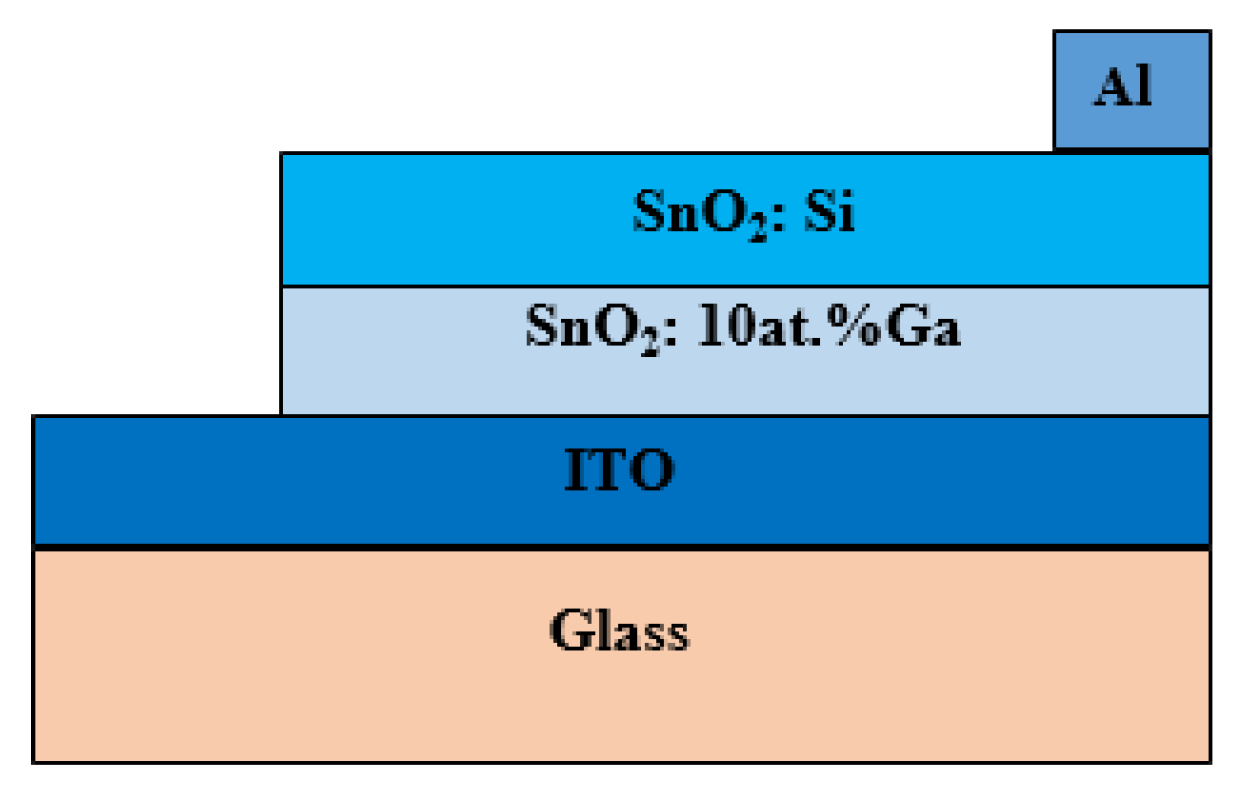
2. Materials and Methods
3. Results and Discussion
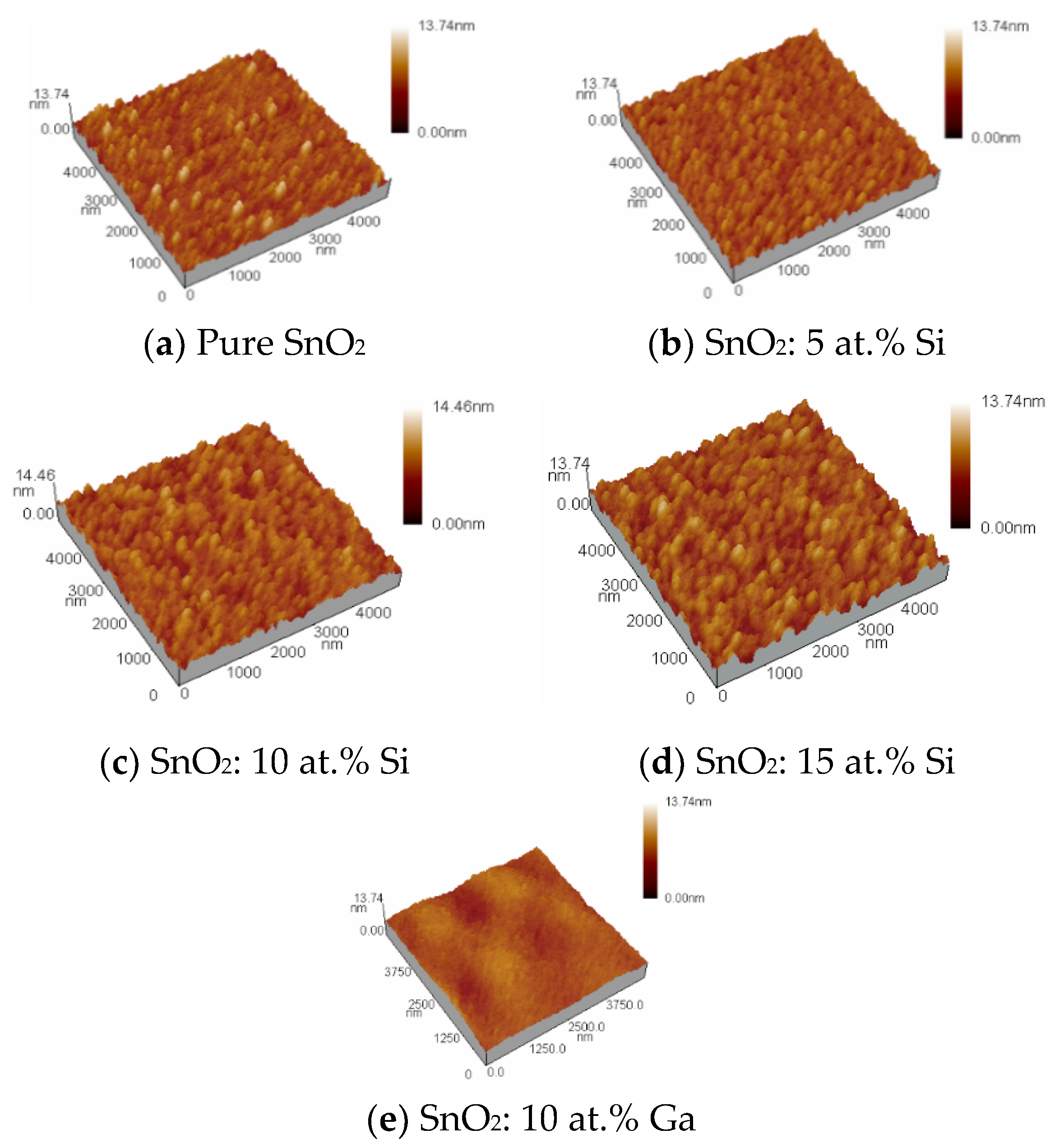
3.1. Film Morphology
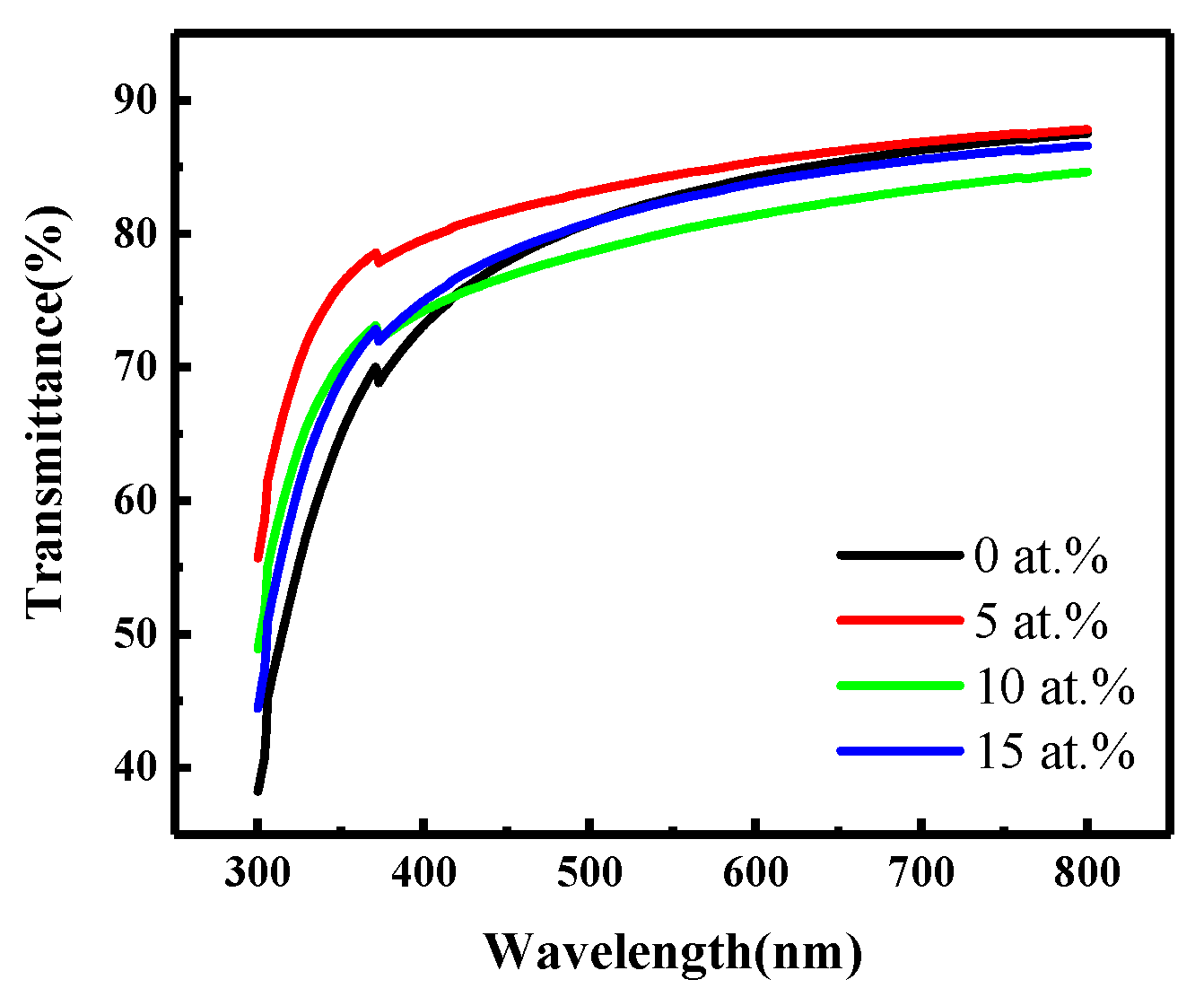
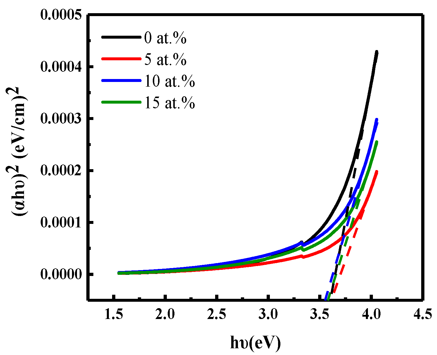
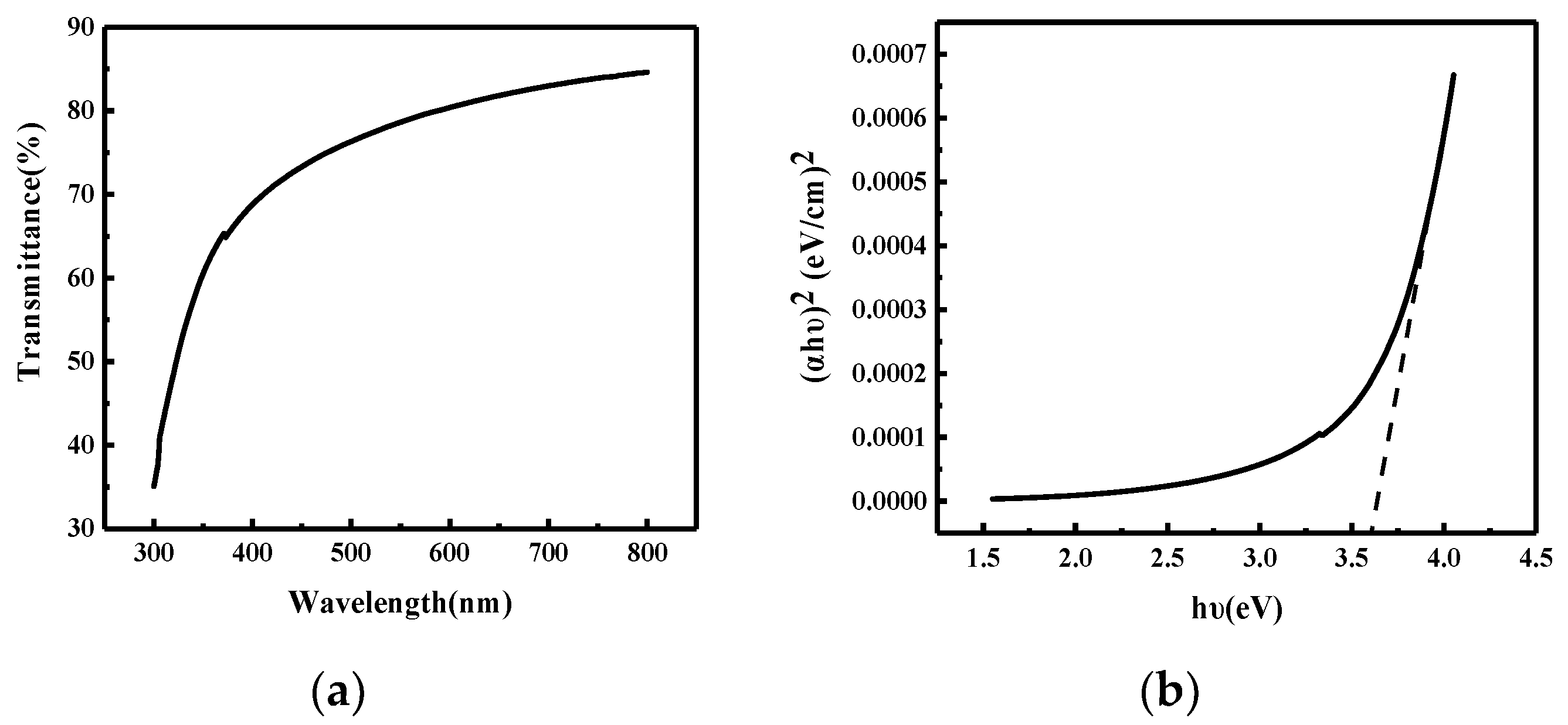
3.2. Optical Characterization
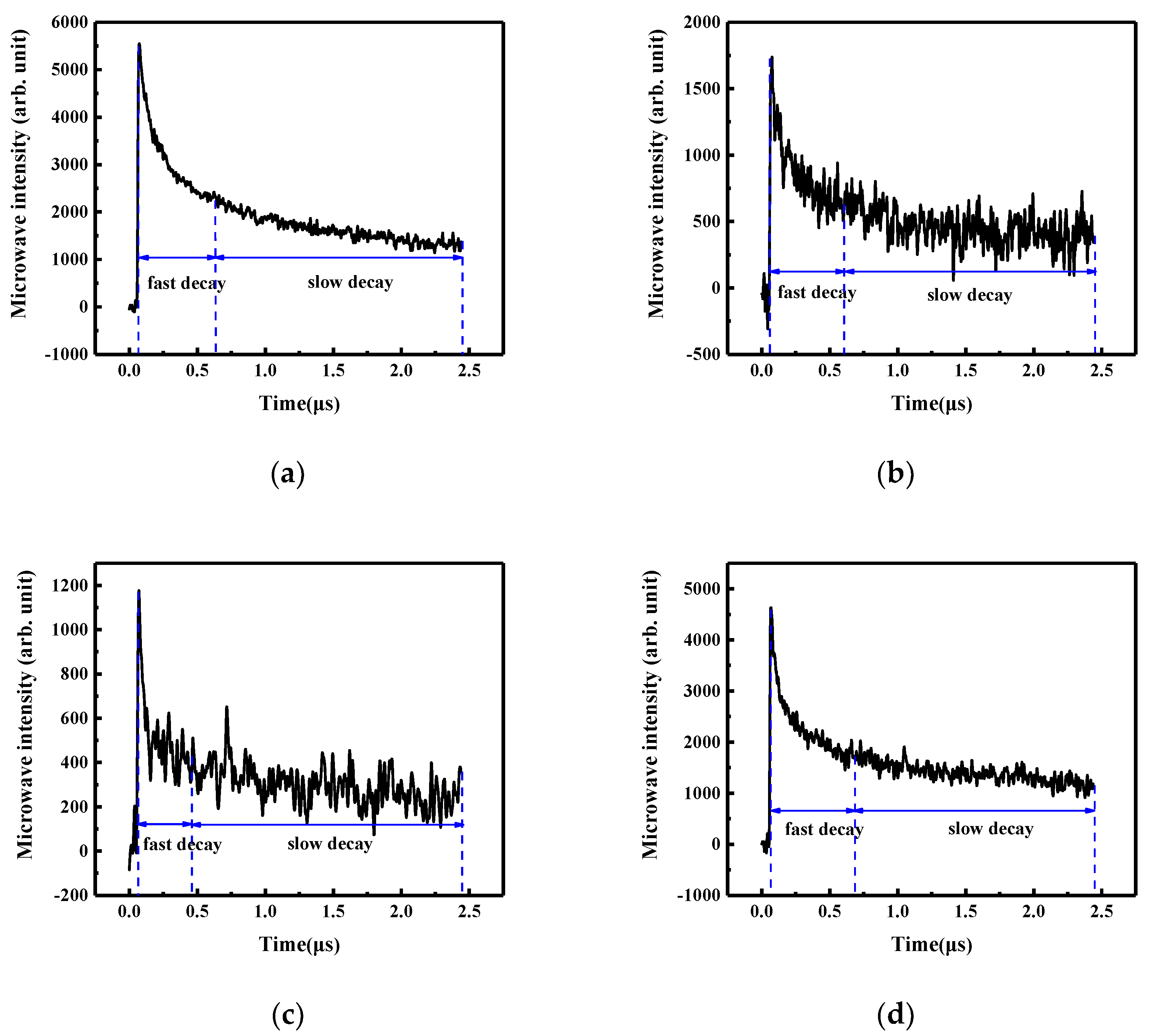
3.3. Characterization of Semiconductor Properties of Thin Films
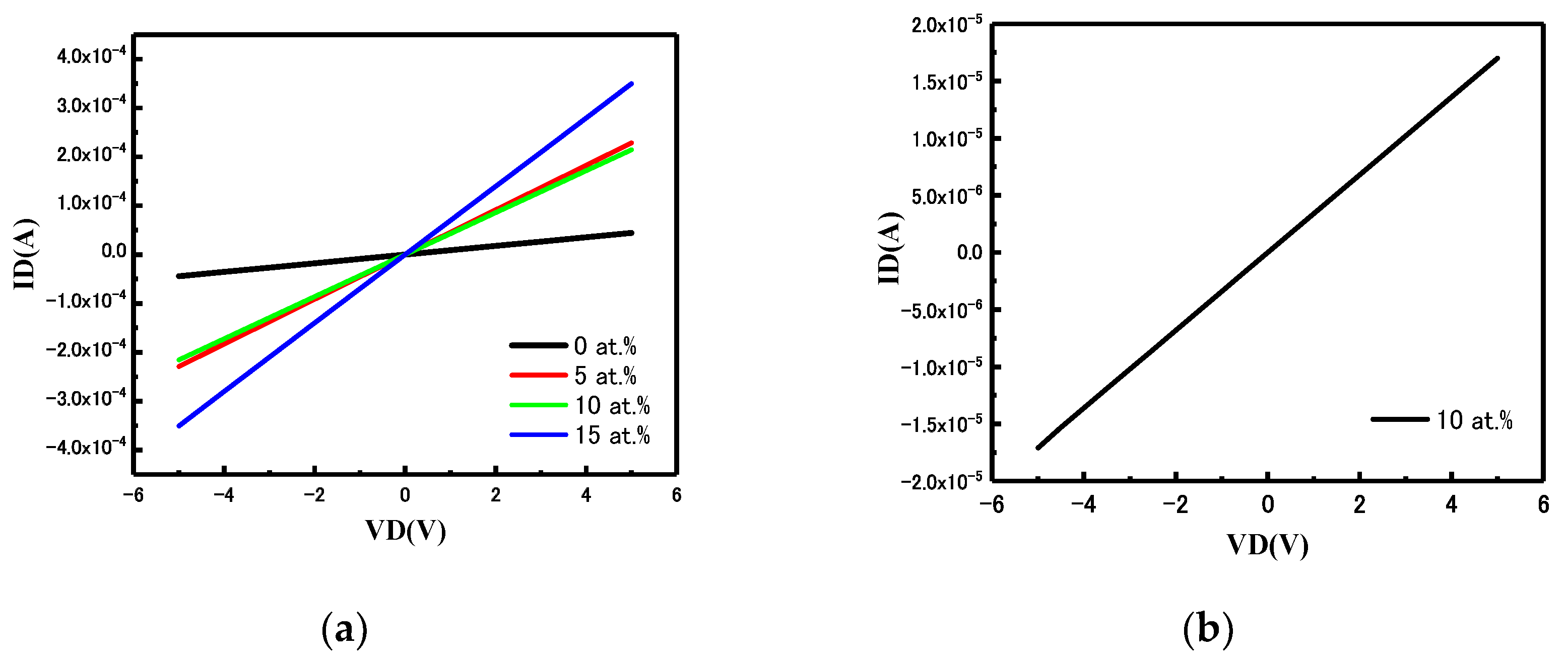
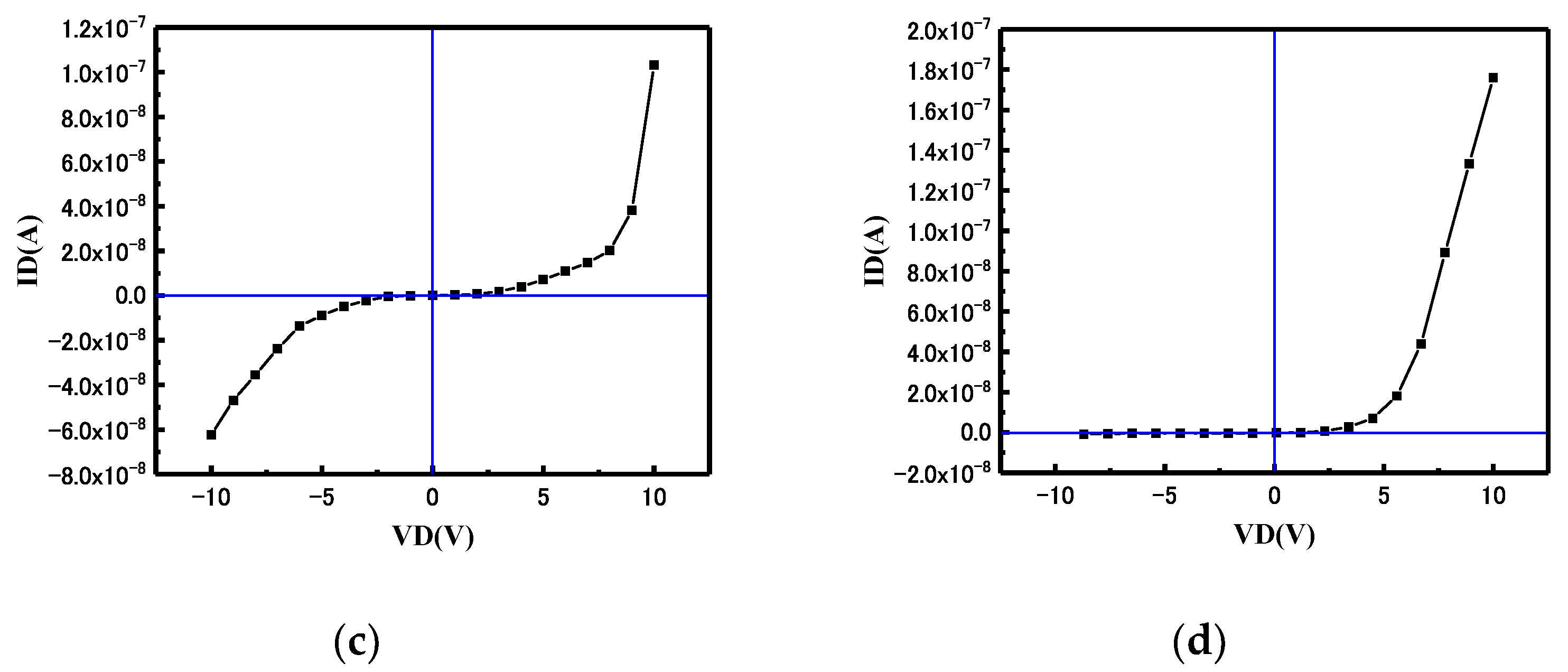
3.4. Characterization of SnO2 Homojunction with Different Si Doping Concentrations
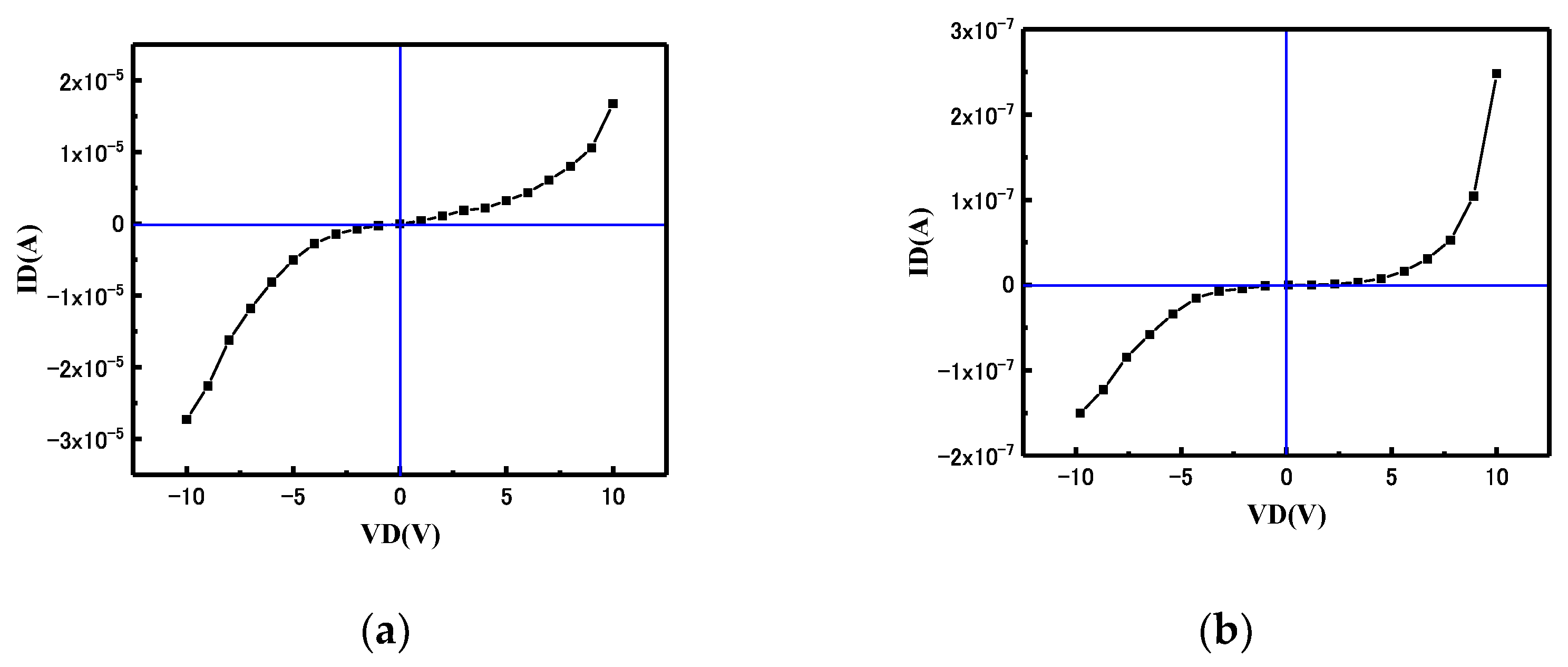
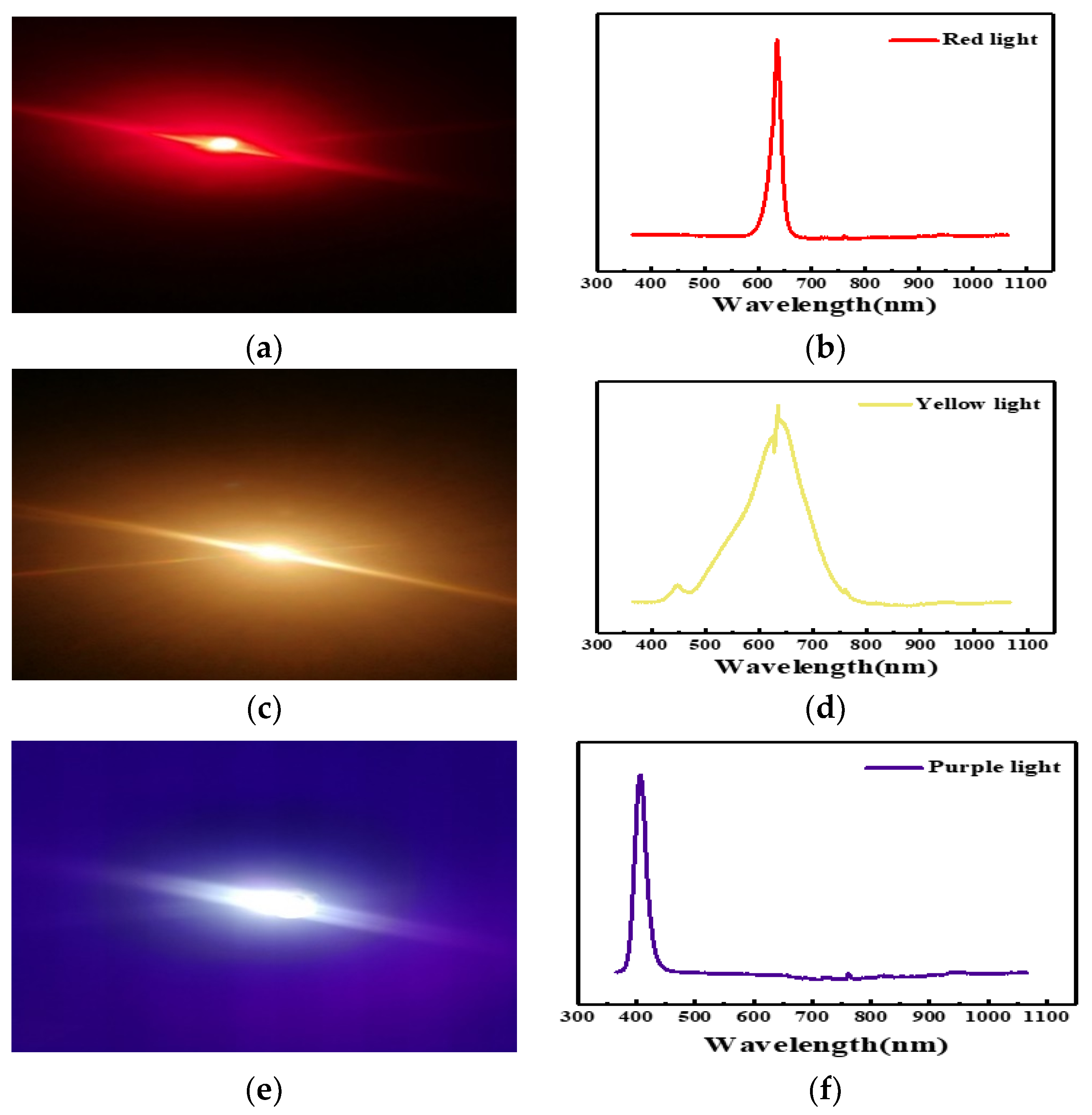
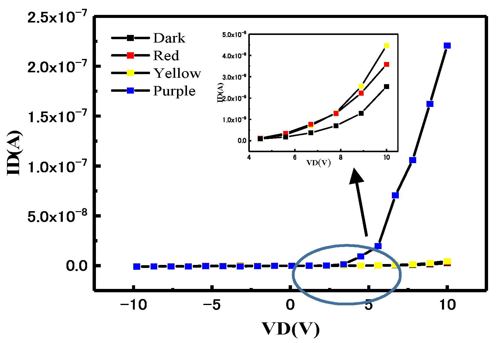
3.5. Current Response of SnO2 Homojunction under Different Frequency Lights
4. Conclusions
Author Contributions
Funding
Conflicts of Interest
References
- Baek, J.H.; Kim, B.J.; Han, G.S.; Hwang, S.W.; Kim, D.R.; Cho, I.S.; Jung, H.S. BiVO4/WO3 /SnO2 Double-Heterojunction Photoanode with Enhanced Charge Separation and Visible-Transparency for Bias-Free Solar Water-Splitting with a Perovskite Solar Cell. ACS Appl. Mater. Inter. 2017, 9, 1479–1487. [Google Scholar] [CrossRef] [PubMed]
- Horng, R.; Shen, K.; Yin, C.; Huang, C.; Wuu, D. High performance of Ga-doped ZnO transparent conductive layers using MOCVD for GaN LED applications. Opt. Express 2013, 21, 14452. [Google Scholar] [CrossRef] [PubMed]
- Ou, S.L.; Wuu, D.S.; Liu, S.P.; Fu, Y.C.; Huang, S.C.; Horng, R.H. Pulsed laser deposition of ITO/AZO transparent contact layers for GaN LED applications. Opt. Express 2011, 19, 16244. [Google Scholar] [CrossRef] [PubMed]
- Abbas, S.; Ban, D.; Kim, J. Functional interlayer of In2O3 for transparent SnO2/SnS2 heterojunction photodetector. Sens. Actuators A Phys. 2019, 293, 215–221. [Google Scholar] [CrossRef]
- He, J.; Wu, J.; Hu, S.; Shen, H.; Hu, X. A low-cost flexible broadband photodetector based on SnO2/CH3NH3PbI3 hybrid structure. Opt. Mater. 2019, 88, 689–694. [Google Scholar] [CrossRef]
- Gao, C.; Li, X.; Zhu, X.; Chen, L.; Wang, Y.; Teng, F.; Zhang, Z.; Duan, H.; Xie, E. High performance, self-powered UV-photodetector based on ultrathin, transparent, SnO2–TiO2 core–shell electrodes. J. Alloy. Compd. 2014, 616, 510–515. [Google Scholar] [CrossRef]
- Park, M.; Kim, J.; Son, H.J.; Lee, C.; Jang, S.S.; Ko, M.J. Low-temperature solution-processed Li-doped SnO2 as an effective electron transporting layer for high-performance flexible and wearable perovskite solar cells. Nano Energy 2016, 26, 208–215. [Google Scholar] [CrossRef]
- Sathyamoorthy, R.; Abhirami, K.M.; Gokul, B.; Gautam, S.; Chae, K.H.; Asokan, K. Fabrication of p-n junction diode using SnO/SnO2 thin films and its device characteristics. Electron. Mater. Lett. 2014, 10, 743–747. [Google Scholar] [CrossRef]
- Wang, L.; Yu, J.; Wang, L.; Niu, X.; Fu, C.; Qiu, R.; Yan, W.; Zhao, H. Influence of doping on photoelectric properties of tin dioxide film. J. Silicate 2018, 46, 590–597, (In Chinese with English abstract). [Google Scholar]
- Tsay, C.; Liang, S. Fabrication of p-type conductivity in SnO2 thin films through Ga doping. J. Alloy. Compd. 2015, 622, 644–650. [Google Scholar] [CrossRef]
- Singh, R.; Kumar, M.; Shankar, S.; Singh, R.; Ghosh, A.K.; Thakur, O.P.; Das, B. Effects of Sb, Zn doping on structural, electrical and optical properties of SnO2 thin films. Mater. Sci. Semicon. Proc. 2015, 31, 310–314. [Google Scholar] [CrossRef]
- Pashley, M.D.; Haberern, K.W. Compensating surface defects induced by Si doping of GaAs. Phys. Rev. Lett. 1991, 67, 2697–2700. [Google Scholar] [CrossRef] [PubMed]
- Gubbins, M.A.; Casey, V.; Newcomb, S.B. Nanostructural characterisation of SnO2 thin films prepared by reactive r.f. magnetron sputtering of tin. Thin Solid Films 2002, 405, 270–275. [Google Scholar] [CrossRef]
- Kanai, N.; Nuida, T.; Ueta, K.; Hashimoto, K.; Watanabe, T.; Ohsaki, H. Photocatalytic efficiency of TiO2/SnO2 thin film stacks prepared by DC magnetron sputtering. Vacuum 2004, 74, 723–727. [Google Scholar] [CrossRef]
- Zhou, Y.; Xu, W.; Lv, S.; Yin, C.; Li, J.; Zhu, B.; Liu, Y.; He, C. GaN codoping and annealing on the optoelectronic properties of SnO2 thin films. J. Alloy. Compd. 2018, 732, 555–560. [Google Scholar] [CrossRef]
- Ali, S.M.; Hussain, S.T.; Bakar, S.A.; Muhammad, J.; Rehman, N.U. Effect of doping on the structural and optical properties of SnO2 thin films fabricated by aerosol assisted chemical vapor deposition. J. Phys. 2013, 93, 012013. [Google Scholar]
- Ning, H.; Zhang, X.; Wang, S.; Yao, R.; Liu, X.; Hou, D.; Ye, Q.; Li, J.; Huang, J.; Cao, X.; et al. Preparation and optimization of SnOx thin film by solution method at low temperature. Superlattices Microstruct. 2020, 139, 106400. [Google Scholar] [CrossRef]
- Tauc, J. The Optical Properties of Solids; Academic Press: New York, NY, USA, 1966; p. 277. [Google Scholar]
- Burstein, E. Anomalous Optical Absorption Limit in InSb. Phys. Rev. 1953, 93, 632. [Google Scholar] [CrossRef]
- Thirumoorthi, M.; Prakash, J.T.J. Effect of F doping on physical properties of (211) oriented SnO2 thin films prepared by jet nebulizer spray pyrolysis technique. Superlattices Microstruct. 2016, 89, 378–389. [Google Scholar] [CrossRef]
- Cao, Y.; Yang, W.; Zhang, W.; Liu, G.; Yue, P. Improved photocatalytic activity of Sn4+ doped TiO2 nanoparticulate films prepared by plasma-enhanced chemical vapor deposition. New J. Chem. 2004, 28, 218. [Google Scholar] [CrossRef]
- Yasuno, S.; Kita, T.; Morita, S.; Hino, A.; Hayashi, K.; Kugimya, T.; Sumie, S. Application of Microwave Photoconductivity Decay Method to Characterization of Amorphous In-Ga-Zn-O Films. IEICE Trans. Electron. 2012, 95, 1724–1729. [Google Scholar] [CrossRef]
- Yao, R.; Zheng, Z.; Xiong, M.; Zhang, X.; Li, X.; Ning, H.; Fang, Z.; Xie, W.; Lu, X.; Peng, J. Low-temperature fabrication of sputtered high-k HfO2 gate dielectric for flexible a-IGZO thin film transistors. Appl. Phys. Lett. 2018, 112, 103503. [Google Scholar] [CrossRef]
- Gao, D.; Lu, Q.; Wei, Y.; Huang, B. Measurement of minority carrier lifetime of n-type 4H-SiC by microwave photoconductive attenuation. Laser Tech. 2011, 35, 610–612, (In Chinese with English abstract). [Google Scholar]
- Liu, X.; Cai, W.; Chen, J.; Fang, Z.; Ning, H.; Hu, S.; Tao, R.; Zeng, Y.; Zheng, Z.; Yao, R.; et al. A novel nondestructive testing method for amorphous Si–Sn–O films. J. Phys. D Appl. Phys. 2016, 49, 505102. [Google Scholar] [CrossRef]
- Yasuno, S.; Kita, T.; Morita, S.; Kugimiya, T.; Hayashi, K.; Sumie, S. Transient photoconductivity responses in amorphous In-Ga-Zn-O films. J. Appl. Phys. 2012, 112, 053715. [Google Scholar] [CrossRef]
- Zhang, X.; Liu, X.; Lu, K.; Ning, H.; Guo, D.; Wang, Y.; Li, Z.; Shi, M.; Yao, R.; Peng, J. The Performance of Zr-Doped Al-Zn-Sn-O Thin Film Transistor Prepared by Co-Sputtering. Appl. Sci. 2019, 9, 5150. [Google Scholar] [CrossRef]
- Wei, J.; Fang, Z.; Peng, J.; Cai, W.; Zhu, Z.; Yao, R.; Zhou, S.; Yuan, W.; Lu, K.; Ning, H. High-performance spin-coated aluminum oxide dielectric fabricated by a simple oxygen plasma-treatment process. J. Phys. D Appl. Phys. 2018, 51, 365101. [Google Scholar] [CrossRef]
- Geng, S. Preparation and Study of p-type Conductive Transparent Tin Dioxide Film and Its PN Junction. Master’s Thesis, Wuhan University of Technology, Wuhan, China, 2012. (In Chinese with English abstract). [Google Scholar]
- Zhang, X.L.; Hui, K.S.; Hui, K.N. High photo-responsivity ZnO UV detectors fabricated by RF reactive sputtering. Mater. Res. Bull. 2013, 48, 305–309. [Google Scholar] [CrossRef]


| Si Doping Concentrations | Transmittance (at 560 nm) (%) | Band Gap (eV) |
|---|---|---|
| 0 at.% | 83.1 | 3.60 |
| 5 at.% | 84.6 | 3.61 |
| 10 at.% | 80.4 | 3.56 |
| 15 at.% | 82.8 | 3.58 |
| Thin Films | Pure SnO2 | SnO2:5 at.% Si | SnO2:10 at.% Si | SnO2:15 at.% Si |
|---|---|---|---|---|
| Mean peak(mV) | 36.3 | 14.5 | 17.0 | 58.6 |
| D value | 0.321 | 0.234 | 0.276 | 0.260 |
| Minority carrier lifetime (μs) | 0.528 | 0.547 | 0.424 | 0.626 |
© 2020 by the authors. Licensee MDPI, Basel, Switzerland. This article is an open access article distributed under the terms and conditions of the Creative Commons Attribution (CC BY) license (http://creativecommons.org/licenses/by/4.0/).
Share and Cite
Ye, Q.; Zhang, X.; Guo, D.; Xu, W.; Ning, H.; Qiu, T.; Li, J.; Hou, D.; Yao, R.; Peng, J. Preparation of Highly Transparent (at 450–800 nm) SnO2 Homojunction by Solution Method and Its Photoresponse. Coatings 2020, 10, 399. https://doi.org/10.3390/coatings10040399
Ye Q, Zhang X, Guo D, Xu W, Ning H, Qiu T, Li J, Hou D, Yao R, Peng J. Preparation of Highly Transparent (at 450–800 nm) SnO2 Homojunction by Solution Method and Its Photoresponse. Coatings. 2020; 10(4):399. https://doi.org/10.3390/coatings10040399
Chicago/Turabian StyleYe, Qiannan, Xu Zhang, Dong Guo, Wei Xu, Honglong Ning, Tian Qiu, Jinxiong Li, Danqing Hou, Rihui Yao, and Junbiao Peng. 2020. "Preparation of Highly Transparent (at 450–800 nm) SnO2 Homojunction by Solution Method and Its Photoresponse" Coatings 10, no. 4: 399. https://doi.org/10.3390/coatings10040399
APA StyleYe, Q., Zhang, X., Guo, D., Xu, W., Ning, H., Qiu, T., Li, J., Hou, D., Yao, R., & Peng, J. (2020). Preparation of Highly Transparent (at 450–800 nm) SnO2 Homojunction by Solution Method and Its Photoresponse. Coatings, 10(4), 399. https://doi.org/10.3390/coatings10040399