Article

GLAD Magnetron Sputtered Ultra-Thin Copper Oxide Films for Gas-Sensing Application

by
Artur Rydosz
1,
Katarzyna Dyndał
1,*,
Wojciech Andrysiewicz
2,
Dominik Grochala
3 and
Konstanty Marszałek
1
1
Department of Electronics, AGH University of Science and Technology, Al. Mickiewicza 30,30-059 Krakow, Poland
2
CBRTP S.A., ul. L. Waryńskiego 3A, 00-645 Warszawa, Poland
3
Department of Biocybernetics and Biomedical Engineering, AGH University of Science and Technology, Al. Mickiewicza 30,30-059 Krakow, Poland
*
Author to whom correspondence should be addressed.
Coatings 2020, 10(4), 378; https://doi.org/10.3390/coatings10040378
Submission received: 2 March 2020 / Revised: 25 March 2020 / Accepted: 9 April 2020 / Published: 11 April 2020
(This article belongs to the Special Issue Metal Oxide Films and Their Applications)

Abstract

:
Copper oxide (CuO) ultra-thin films were obtained using magnetron sputtering technology with glancing angle deposition technique (GLAD) in a reactive mode by sputtering copper target in pure argon. The substrate tilt angle varied from 45 to 85° and 0°, and the sample rotation at a speed of 20 rpm was stabilized by the GLAD manipulator. After deposition, the films were annealed at 400 °C/4 h in air. The CuO ultra-thin film structure, morphology, and optical properties were assessed by X-ray diffraction (XRD), energy-dispersive X-ray spectroscopy (EDX), X-ray reflectivity (XRR), and optical spectroscopy. The thickness of the films was measured post-process using a profilometer. The obtained copper oxide structures were also investigated as gas-sensitive materials after exposure to acetone in the sub-ppm range. After deposition, gas-sensing measurements were performed at 300, 350, and 400 °C and 50% relative humidity (RH) level. We found that the sensitivity of the device is related to the thickness of CuO thin films, whereas the best results are obtained with an 8 nm thick sample.

1. Introduction

Gas sensors have been investigated over the last few decades, and the first gas sensor was introduced to the market in 1968 by Figaro Company. It is still available. Since then, the gas sensor market has increased year by year, and it is expected to be worth USD 1.4 billion in 2024 [1]. Generally, a gas sensor consists of gas-sensitive films and gas sensor substrate with electrodes, a package, and front-end electronic circuits. The gas-sensitive layer can be realized based on various materials, including organic compounds (e.g., phthalocyanines [2,3]) and metal oxides [4] (e.g., WO3 [5,6], TiO2 [7,8], SnO2 [9,10], In2O3 [11,12], Fe2O3 [13,14], MoO3 [13,15], ZnO [16,17,18], CuO [19,20,21,22,23,24,25,26,27,28]). The most common methods for metal oxide depositions are magnetron sputtering [29,30], sol–gel [31,32], thermal oxidation [33,34], hydrothermal techniques [35,36], the spray pyrolysis technique [37,38], and the microwave-assisted method [39,40]. Among them, magnetron sputtering is widely accepted for industrial purposes, because it can be easily adapted to Complementary Metal Oxide Semiconductor (CMOS) technology; therefore, front-end electronics compounds can be realized by using the same technology. Gas sensors are characterized by the “3-S” parameters: sensitivity, selectivity, and stability. Gas-sensitive layers play an important role in all of these parameters. For instance, sensitivity is related to the surface–volume ratio of the gas-sensitive layer; therefore, the nanocolumnar structure is preferred compared to conventional thin film deposition [41]. Nanocolumnar structures, such as nanorods, nanowires, nanofibers, and nanotubulars, can be realized in various techniques; however, in magnetron sputtering technology, two techniques are used: template and template-free, e.g., glancing angle deposition technique (GLAD) [42]. The advantage of the template-free method compared to the template method is the reduction of the technological steps, and the GLAD technique offers the possibility to deposit various nanocolumnar structures [41]. This method involves a deposition at oblique angles, where the trajectory of the incident vapor flux is not parallel to the substrate normal. The GLAD process requires changing both the angle of the substrate and the rotation rate during deposition, which allows for controlling the column dimension and the overall thickness of the films. Recently, the GLAD technique was applied for the deposition of metal oxides for gas-sensing applications, such as WO3 [43], SnO2 [44,45,46], NiO [44], SiO2 [47], and In2O3 [48]. The advantages of GLAD deposition in these applications have been presented and discussed. The GLAD technique can be used for the deposition of CuO films, but there are only a few studies regarding their deposition using the GLAD method. Tounsi et al. [49] fabricated Cu2O/CuO films by depositing Cu thin films at various angles α (0÷80°), using the GLAD technique, and then annealing them in free air. For layers annealed at 200 °C, the obtained results from XRD and Raman measurements showed Cu2O, CuO, and metallic Cu phases. After annealing at 300 °C, the layers obtained a CuO monophase. Band gap, Urbach energies, and optical parameters were estimated from optical absorption data. Correlations between these properties and annealing temperature and deposition angle were examined. The obtained results were consistent with the results of other researchers. In [50], Chaffar Akkari et al. described the fabrication of CuOx films on glass substrate by air annealing copper thin films deposited by thermal evaporation method using the GLAD technique. In this work, the morphological, structural, optical, and electrical properties were measured. The results show that GLAD is a very good technique to create such films, which have a polycrystalline nature where crystallite size decreases when the deposition angle is higher. It was shown that the obtained layers have an absorption coefficient higher than 105 cm−1 in the visible range. In the case of the band gap and the Urbach energy, which increase with the increasing of the incident deposition angle, their values range from 2 to 2.54 eV and from 259 to 534 meV, respectively. Additionally, studies have shown electrical anisotropy of layers.
In this paper, the investigation provides results on copper oxides deposited by a commercially available glancing angle deposition system (most papers present only the investigation on homemade GLAD manipulators, which reduce the possibility of repeating the results) at various conditions. The deposited thin films were used as gas-sensitive layers for sub-ppm acetone detection, which is recognized to be a biomarker of diabetes present in the breath [51,52,53,54,55,56].

2. Materials and Methods
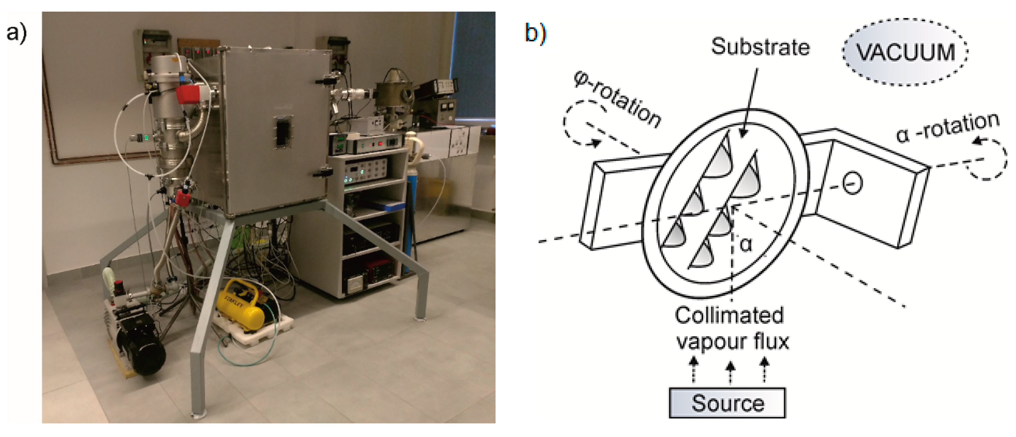
2.1. CuO Deposition

The copper oxide thin films were obtained in the commercially available magnetron sputtering deposition system from Kurt J. Lesker Company (Hastings, Easy Sussex, UK). The system is based on the ECR (ECR-UHV-20532-001) manipulator with a dedicated vacuum chamber equipped with three magnetron sources that allows for the depositing of metals and oxides (Figure 1a).
During these experiments, a copper target (Kurt J. Lesker Company) of 50 mm diameter (5N purity) was employed for reactive sputtering at various argon/oxygen mixtures, such as 66%O2/34%Ar, 80%O2/20%Ar, 100%O2/0%Ar. The flows of argon and oxygen were controlled by mass flow controllers (MFC) 1179B (MKS Instruments (Andover, MA, USA). The substrate tilt angle varied from 45° to 85° and 0° (Table 1), and the sample rotation at a speed of 20 rpm was stabilized by the ECR manipulator. The CuO thin films were deposited onto silicon substrates (Si-Mat, Kaufering, Germany), quartz JGS-2 (Continental Trade, Warsaw, Poland), and BVT (Praha, Czech Republic) for XRD, optical, SEM, and gas-sensing measurements, respectively.
Figure 1b shows a schematic drawing of the GLAD deposition system. The system has been pre-pumped to a vacuum level of 5 × 10⁻⁶ mbar and then to a deposition vacuum level of 3 × 10⁻² mbar. The copper target was first presputtered in pure argon for 10 min at 50 W to remove any contamination, and then, oxygen was introduced into the chamber. After the presputtering processes, the power and temperature were fixed at 50 W and 400 °C, respectively. The sputtering time was adjusted to deposit films with various thicknesses. The copper oxide thin films were fabricated with DC-MF sputtering mode by a power supply from DORA Power System. After deposition, the samples were annealed at 400 °C/4 h in air.

2.2. XRD/XRR Measurements

X-ray diffractometry and X-ray reflectometry were obtained by utilization of X’Pert PRO MPD PANalytical system with a grazing angle of 3° using monochromatic Cu Kα1 radiation. The thickness and density ρ calculations were performed by fitting the XRR data using dedicated software. The film thickness and density were obtained by the period of oscillations in the XRR curve and the position of the total reflection edge, respectively.

2.3. SEM/EDX Measurements

The structure of the CuO films was observed in a scanning electron microscope equipped with an electron backscatter diffraction mode (Nova NANOSEM 200, FEI, Hillsboro, OR, USA) with an attachment for the detection of characteristic X-ray radiation (EDS, EDAX Genesis).

2.4. Optical Measurements

Optical measurements were carried out with the Perkin-Elmer double-beam spectrophotometer Lambda 19. The spectra of the transmission coefficient were recorded within the wavelength range from 300 to 2200 nm with a step of 1 nm.

2.5. Thickness Measurements

The CuO film thicknesses determination was carried out using a Taly-step profilometer (Taylor Hobson, Leicester, UK.)

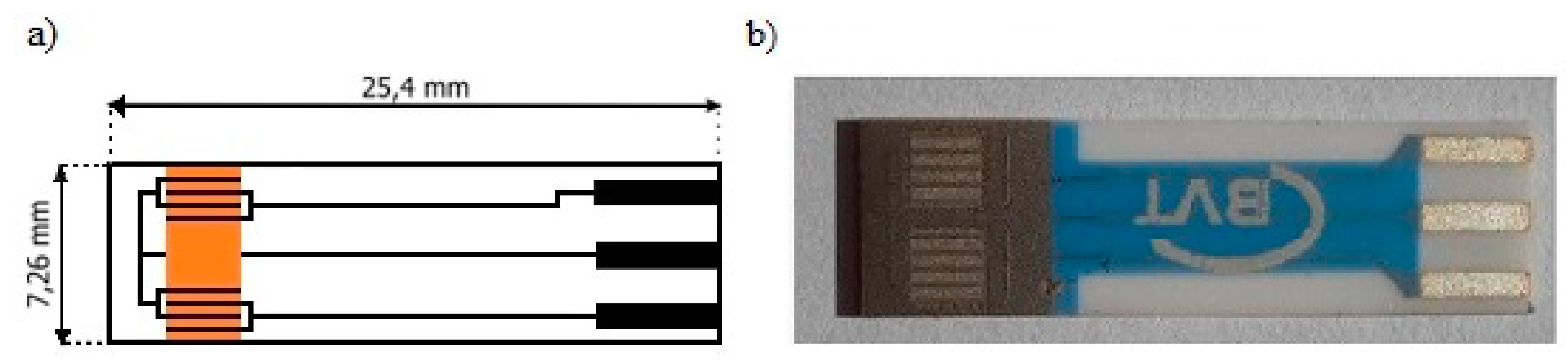
2.6. Gas-Sensing Setup

The gas-sensing setup was previously described in [51,52,56]. Briefly, the developed sensors (Figure 2a,b) with various copper oxides serve as the gas-sensitive layers, which were placed in the quartz-tube oven, and the target gas at various concentrations was introduced.
Because the measurements were based on the measurements of the electrical resistance changes, an electrometer (34401A HP) was used to record the electrical resistance of the sensor under exposure to air and target gas. Therefore, the gas sensor response (S) was defined as the resistance ratio S = (Rgas − Rair)/Rair, where Rgas and Rair are electrical resistances in gas and air, respectively. By using specialized mass flow controllers 1179B (MKS Instruments, Andover, MA, USA), different concentration levels were obtained. A gas mixture (Air Products, Hersham, UK) containing 5 ppm of acetone, 20.944% mol of oxygen, and 79.054% mol of nitrogen was used for the measurements. Measurements to detect gas were carried out at various temperatures and 50% relative humidity (RH) level. All the methods used to characterize the copper oxide layers obtained by means of the GLAD technique are shown in Table 2.

3. Results and Discussion

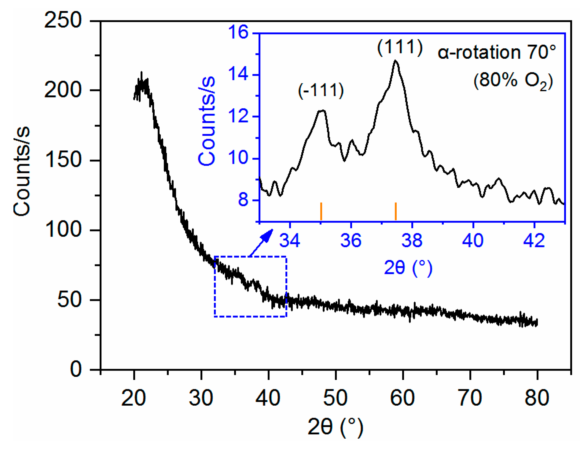
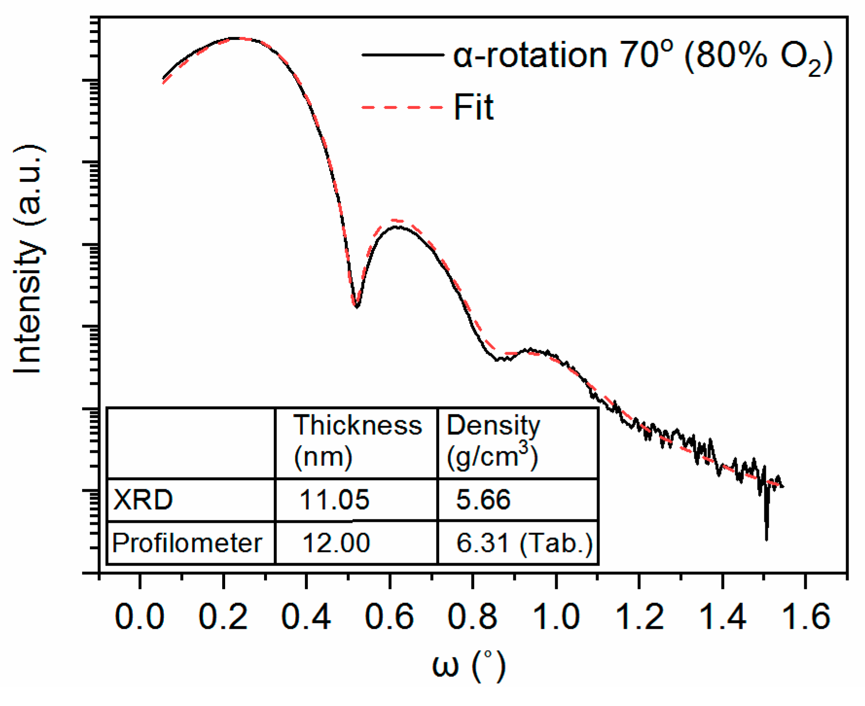
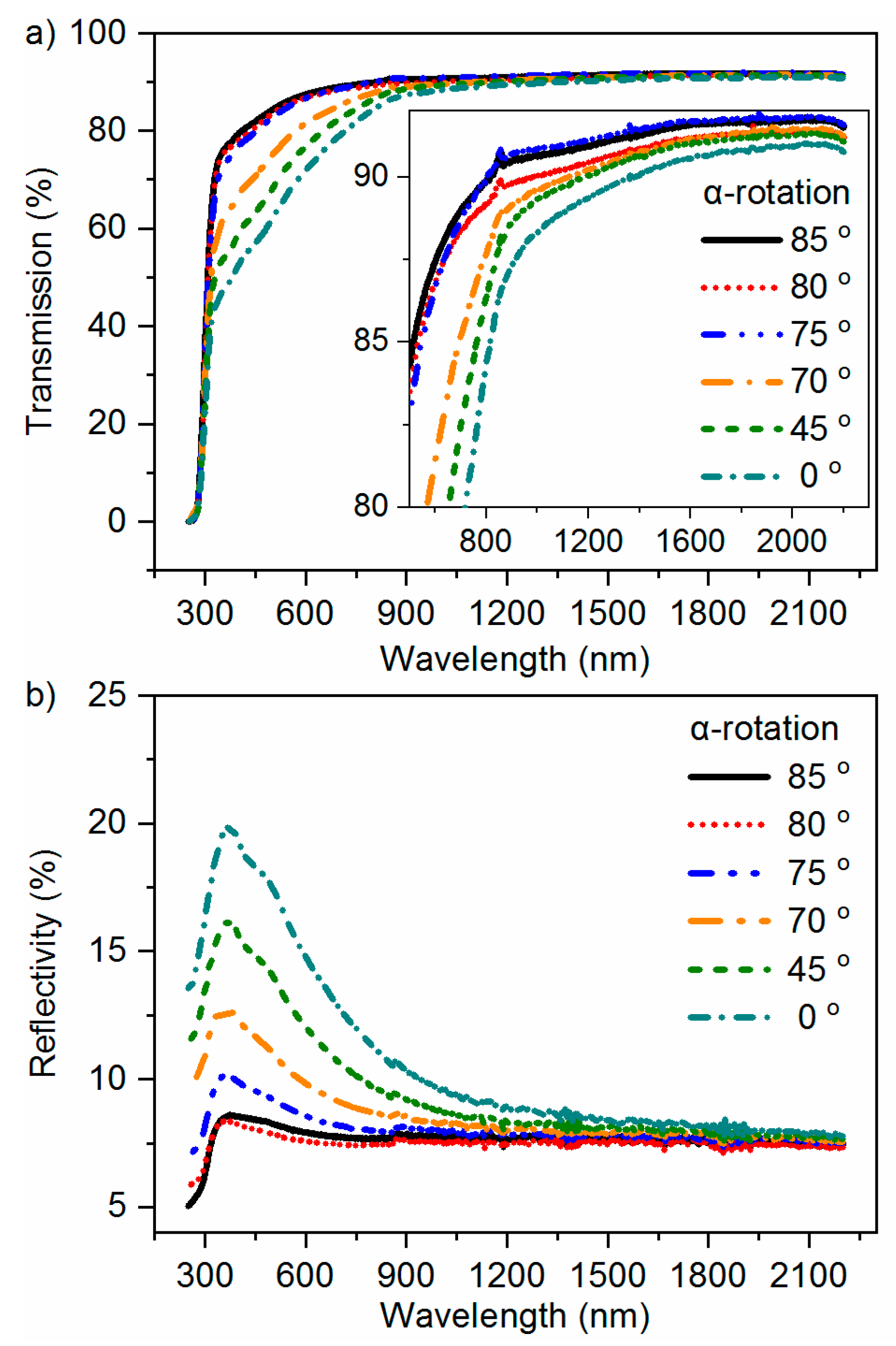
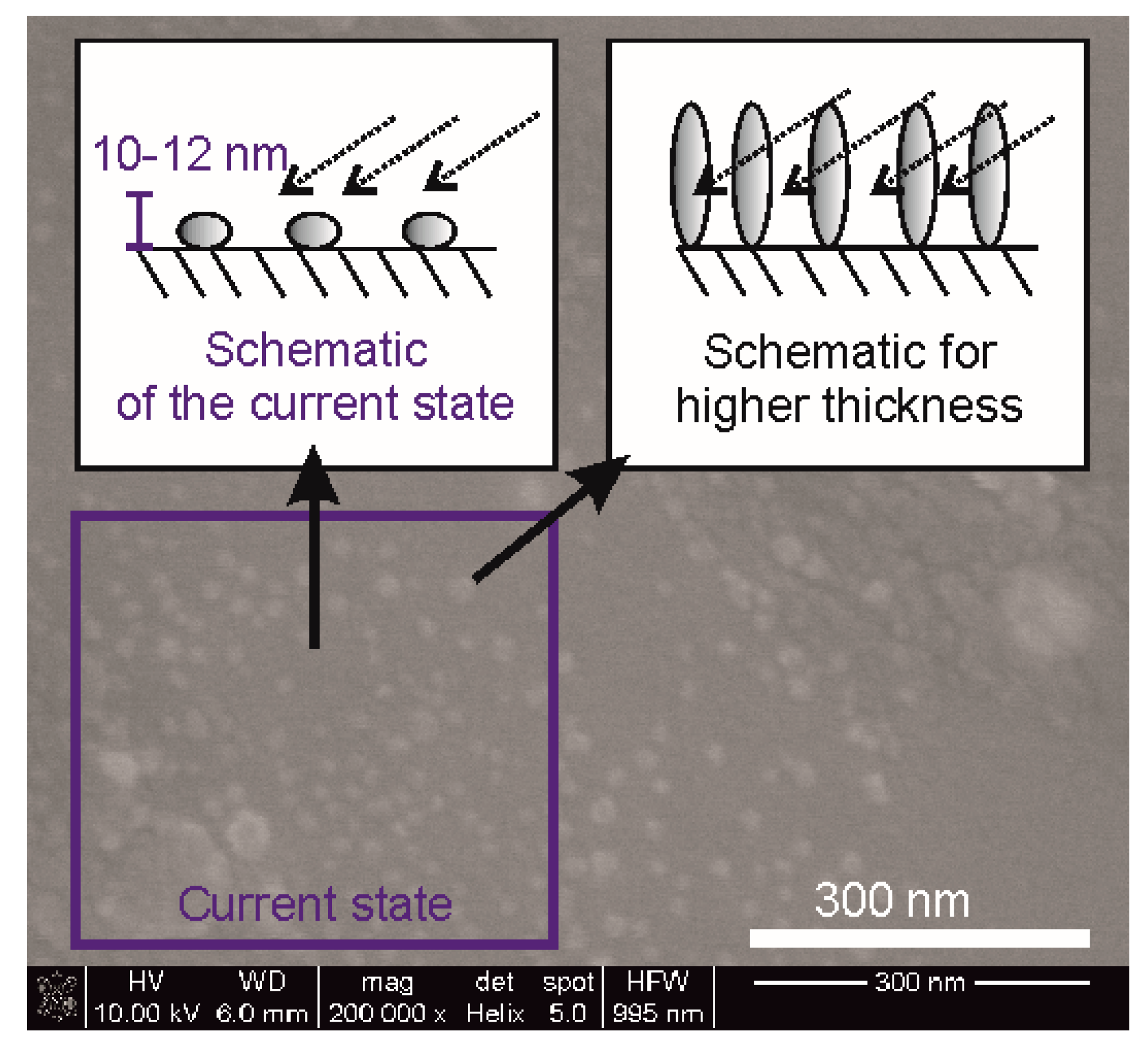
3.1. Material Characterization Results

The crystallographic structure of the deposited gas-sensing layers was determined with X-ray diffraction and reflectivity. However, it is important to note that ultra-thin films were deposited; therefore, the special adapter was used by the XRD system to measure the diffraction of deposited films at the grazing angle of 3° using monochromatic Cu Kα1 radiation. Figure 3 shows the XRD experiment results, where low-intensity peaks were observed at 35.05° and 37.45°. They correspond to the (−111) and (111) crystal of the CuO phase. The intensities and positions of the peaks are in good agreement with the reported values ICDD #01-080-1916. Figure 4 shows the XRR measurement results for copper oxide film deposited at a 70° angle and 80% content of O2 in the reactive atmosphere of argon/oxygen. The thickness calculated from the XRR results is in agreement with the thickness measured by the mechanical profilometer, i.e., 11.05 nm and 12.00 nm, respectively. The difference can be observed between the density value estimated from measurement and from the theoretical, i.e., 5.66 g/cm3 and 6.31 g/cm3. However, it has to be taken into account that the theoretical density of CuO was obtained for CuO powders [57,58]. Shehayeb et al. [59] found the variation of density values for CuO films deposited by an electrophoretic deposition (EPD) based on dispersed CuO nanoparticles, where density was in the range of ~3.3–4.5 g/cm3. Chuagan et al. [60] presented the investigation results on nanostructured CuO prepared via sol–gel method, where density ranged from 2.16 to 2.56 g/cm3.
Apart from gas-sensing applications, CuO is also an attractive material for optical applications; therefore, the basic optical properties, such as transmission and reflectivity, were measured. The results are presented in Figure 5. As can be observed, the transmission of the films increased from 20% to 90%. The highest transmission was obtained from the thinnest films deposited with the 85°, 80°, and 75° substrate tilt angles. The reflectivity of all the obtained CuO films was less than 20% and higher than 7% through most of the spectral region. The highest reflectivity was assigned to the thin films deposited with 0°, 45°, and 70° substrate tilt angles.
The morphology of all the copper oxide films was investigated using scanning electron microscopy. Each film showed the same morphology. As a result, in Figure 6, only one example was shown. The films were deposited using the GLAD technique; therefore, the shadowing effect can be observed. The main aim of the paper was to verify the acetone detection by ultra-thin copper oxides, and therefore, 8–15 nm thin films were deposited (refer to Figure 8). Increasing the deposition time would lead to increasing the thickness, as shown schematically in Figure 6. The GLAD technique allows for the possibility of controlling the nanocolumnar growth, including the spacing between the nucleation as presented in the SEM photo. However, further optimization is needed, where the substrate tilt angle, substrate rotation, substrate temperature, argon/oxygen mixture, and other deposition parameters are selected.

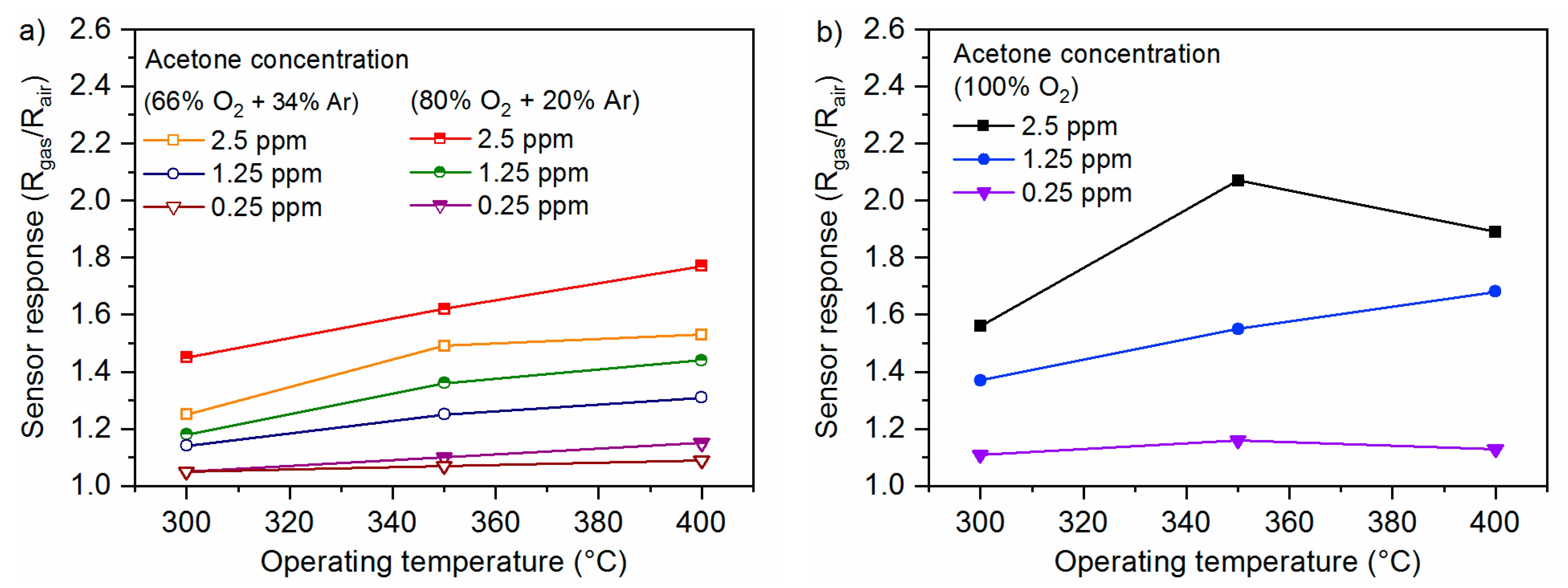
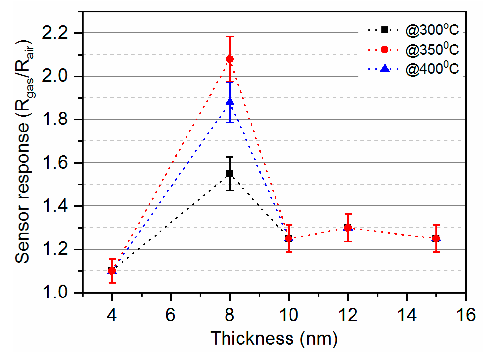
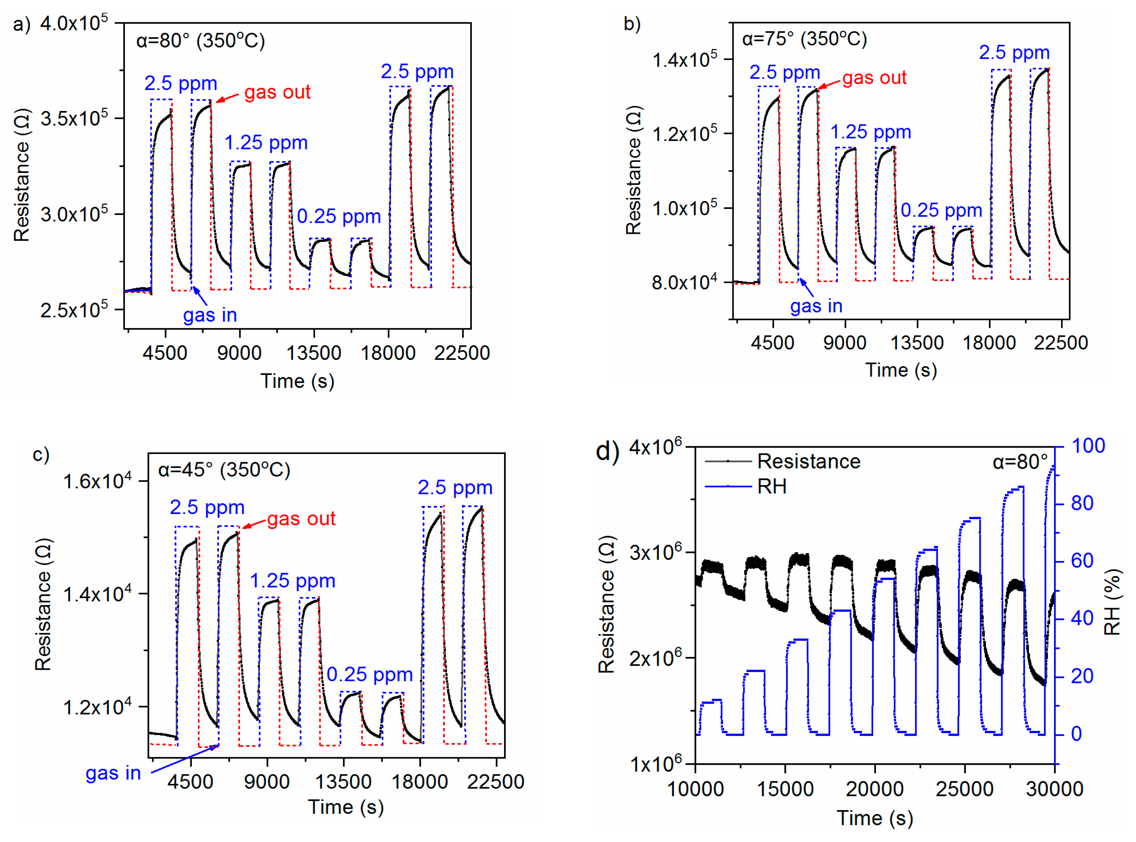
3.2. Gas-Sensing Characteristics

Working temperature is one of the main factors that affect the response of gas sensors based on metal oxides. Figure 7 shows the sensor response (Rgas/Rair) measured at 0.25, 1.25, and 2.5 ppm of acetone vs. the operating temperature for copper oxides deposited at 66%O2/34%Ar and 80%O2/20%Ar, respectively (Figure 7a), and 100%O2 content (Figure 7b) in the reactive atmosphere. This shows that the highest responses were obtained at 350 °C for layers deposited at 100%O2 (fully reactive mode). Generally, 350 °C was the operating temperature with the highest responses; however, in some cases, the results obtained indicated that an operating temperature above 400 °C could give better results. Due to the limitation of the gas-sensing system, such measurements could not be carried out. Moreover, from a practical point of view, the operating temperature should be as low as possible to reduce the power consumption needed to heat up the sensors. A solution to reduce the power consumption could be found in the literature [62,63]. The reaction of oxygen with an adsorption site results in O- and the generation of a hole, which leads to an accumulation layer at the surface of the p-type conducting metal oxides, such as CuO [64]. The common model for the detection of reducing gases is based on the decrease of oxygen species at the surface leading to an increase of resistance, which was observed when the copper oxide-based sensor was exposed to acetone [65,66].
As was already mentioned, the main goal of the experiment was to define the sensor response based on the ultra-thin copper oxide layer under exposure to sub-ppm acetone concentration. Therefore, the gas-sensitive layers were deposited in the 4–15 nm range, and the responses are presented in Figure 8. It is worth noting that the most sensitive layers to acetone were those with a thickness of 8 nm, which worked at a temperature of 350 °C. Therefore, this thickness was selected for further experiments. The explanation for decreasing the sensor response when the thickness was increasing could lie in the film’s deposition behavior. For lower thicknesses, slow nanocolumnar growth was observed with strictly separated nucleation islands. When the deposition took longer, the thicknesses increased, but at the same time, new nucleation appeared close to the previous one, which resulted in the reduced surface to volume ratio of the gas-sensitive layer and, in fact, reduced sensor response. The effect will reverse above a certain thickness, known as a threshold thickness, and the effect is related to the material that is used, gas sensor substrate, and deposition conditions. Therefore, the threshold thickness can only be experimentally determined.
As mentioned in the Introduction, higher acetone levels are characteristic of diabetics. For healthy people, the level of acetone in exhaled air is below 1 ppm. In contrast, diabetic acetone levels range from 1.5 to 2.5 ppm. Based on the literature review, both proposed regions are not strictly defined; therefore, the acetone detection has to be carried out in a wide range of concentrations. It should be pointed out that commercially available gas sensors have a limit of detection in tens of ppm for acetone (i.e., Figaro TGS 822: 50–5000 ppm). Figure 9 presents the gas sensor calibration curves. The various gas-sensitive layers (66%O2/34%Ar, 80%O2/20%Ar, and 100%O2 refer to the content of oxygen in the argon/oxygen mixture during the layers deposition) were investigated. As can be observed, the limit of detection was 0.25 ppm, which covers the acetone concentration in the exhaled human breath for healthy people, which is generally in the 0.3–0.9 ppm range.
The gas-sensing characteristics of CuO-based gas sensors under exposure to various acetone concentrations in time function, with gas-in/gas-out phases, are presented in Figure 10a–c. Figure 10d presents the influence of the resistance changes to various relative humidity concentrations, which influences the gas-sensing behavior of the metal oxide-based gas sensors. The fact that the gas-sensing performance of thin film-based sensors is correlated with humidity is widely known. The effect of RH will decrease the total gas sensor response. Moreover, the relative humidity is above 80% in the exhaled breath, and therefore, it always has to be taken into account.

4. Conclusions

In this paper, the investigation results on copper oxide ultra-thin films deposited by a commercially available glancing angle deposition system (magnetron sputtering technology at various conditions) are presented and discussed. The deposited thin films were used as gas-sensitive layers for sub-ppm acetone detection, which is considered to be a biomarker of diabetes present in exhaled breath. The CuO ultra-thin film structure, morphology, and optical properties were assessed by X-ray diffraction, energy-dispersive X-ray spectroscopy, X-ray reflectivity, and optical spectroscopy. The optimal thickness and optimal operating temperatures were 8 nm and 350 °C, respectively. The highest responses were obtained for samples deposited in the fully reactive mode: 100% oxygen during the magnetron sputtering deposition. It was confirmed that sensors can detect acetone as low as 0.25 ppm and that they work well in the 0.25–2.5 ppm range, which covers the exhaled acetone range. However, exhaled breath is fully humidified, and relative humidity above 80% decreases the total gas sensor response. Therefore, relative humidity needs to be reduced by, for instance, applying a humidity trap.

Author Contributions

Conceptualization, A.R.; methodology, A.R. and K.D.; software, W.A. and D.G.; validation, A.R. and K.D.; investigation, A.R., K.D., and W.A.; resources, A.R. and K.D.; writing—original draft preparation, A.R., K.D., and K.M.; writing—review and editing, A.R., K.D., and K.M.; visualization, K.D.; supervision, A.R.; project administration, A.R.; funding acquisition, A.R. All authors have read and agreed to the published version of the manuscript.

Funding

This research was funded by the National Science Centre, Poland 2017/26/D/ST7/00355 and AGH University project 16.16.230.434.

Conflicts of Interest

The authors declare no conflicts of interest.

References

  1. Markets and Markets. Gas Sensors Market by Gas Type (Oxygen, Carbon Monoxide, Carbon Dioxide, Ammonia, Chlorine, Hydrogen Sulfide, Nitrogen Oxide, Volatile Organic Compounds, Hydrocarbons), Technology, Application, Geography—Global Forecast 2024; MarketsandMarkets Research Private Ltd.: Pune, India, November, 2019. [Google Scholar]
  2. Staszek, K.; Rydosz, A.; Maciak, E.; Wincza, K.; Gruszczynski, S. Six-port microwave system for volatile organic compounds detection. Sens. Actuators B Chem. 2017, 245, 882–894. [Google Scholar] [CrossRef]
  3. Jakubik, W.; Krzywiecki, M.; MacIak, E.; Urbańczyk, M. Bi-layer nanostructures of CuPc and Pd for resistance-type and SAW-type hydrogen gas sensors. Sens. Actuators B Chem. 2012, 175, 255–262. [Google Scholar] [CrossRef]
  4. Ji, H.; Zeng, W.; Li, Y. Gas sensing mechanisms of metal oxide semiconductors: A focus review. Nanoscale 2019, 11, 22664–22684. [Google Scholar] [CrossRef] [PubMed]
  5. Rydosz, A.; Szkudlarek, A.; Ziabka, M.; Domanski, K.; Maziarz, W. Performance of Si-doped WO3 thin films for acetone sensing prepared by glancing angle DC magnetron sputtering. IEEE Sens. J. 2015, 16, 1004–1012. [Google Scholar] [CrossRef]
  6. Hariharan, V.; Gnanavel, B.; Sathiyapriya, R.; Aroulmoji, V. A Review on Tungsten Oxide (WO3) and their Derivatives for Sensor Applications. Int. J. Adv. Sci. Eng. 2019, 5, 1163–1168. [Google Scholar] [CrossRef]
  7. Li, F.; Gao, X.; Wang, R.; Zhang, T.; Lu, G. Study on TiO2-SnO2 core-shell heterostructure nanofibers with different work function and its application in gas sensor. Sens. Actuators B Chem. 2017, 248, 812–819. [Google Scholar] [CrossRef]
  8. Li, Z. Resistive-type hydrogen gas sensor based on TiO2: A review. Int. J. Hydrog. Energy 2018, 43, 21114–21132. [Google Scholar] [CrossRef]
  9. Tan, W.; Yu, Q.; Ruan, X.; Huang, X. Design of SnO2-based highly sensitive ethanol gas sensor based on quasi molecular-cluster imprinting mechanism. Sens. Actuators B Chem. 2015, 212, 47–54. [Google Scholar] [CrossRef]
  10. Zhang, D.; Liu, J.; Chang, H.; Liu, A.; Xia, B. Characterization of a hybrid composite of SnO2 nanocrystal-decorated reduced graphene oxide for ppm-level ethanol gas sensing application. RSC Adv. 2015, 5, 18666–18672. [Google Scholar] [CrossRef]
  11. Zhang, S.; Song, P.; Yan, H.; Yang, Z.; Wang, Q. A simple large-scale synthesis of mesoporous In2O3 for gas sensing applications. Appl. Surf. Sci. 2016, 378, 443–450. [Google Scholar] [CrossRef]
  12. Kalantarian, H.; Alshurafa, N.; Sarrafzadeh, M. Detection of Gestures Associated with Medication Adherence Using Smartwatch-Based Inertial Sensors. IEEE Sens. J. 2016, 16, 1054–1061. [Google Scholar] [CrossRef]
  13. Zhang, D.; Fan, X.; Yang, A.; Zong, X. Hierarchical assembly of urchin-like alpha-iron oxide hollow microspheres and molybdenum disulphide nanosheets for ethanol gas sensing. J. Colloid Interface Sci. 2018, 523, 217–225. [Google Scholar] [CrossRef] [PubMed]
  14. Tan, J.; Chen, J.; Liu, K.; Huang, X. Synthesis of porous α-Fe2O3 microrods via in situ decomposition of FeC2O4 precursor for ultra-fast responding and recovering ethanol gas sensor. Sens. Actuators B Chem. 2016, 230, 46–53. [Google Scholar] [CrossRef]
  15. Shen, J. Synthesis of Ni-doped A-MoO3 nanolamella and their improved gas sensing properties. Sens. Actuators B Chem. 2017, 252, 757–763. [Google Scholar] [CrossRef]
  16. Bhati, V.S.; Hojamberdiev, M.; Kumar, M. Enhanced sensing performance of ZnO nanostructures-based gas sensors: A review. Energy Rep. 2019, 6, 46–62. [Google Scholar] [CrossRef]
  17. Pisarkiewicz, T.; Kenig, T.; Rydosz, A.; Maziarz, W. Solution growth of ZnO sub-micro rods enhanced by electric field. Bull. Polish Acad. Sci. Tech. Sci. 2011, 59, 425–428. [Google Scholar] [CrossRef] [Green Version]
  18. Zhu, L.; Zeng, W. Room-temperature gas sensing of ZnO-based gas sensor: A review. Sens. Actuators A Phys. 2017, 267, 242–261. [Google Scholar] [CrossRef]
  19. Ebrahimi, A.; Withayachumnankul, W.; Al-Sarawi, S.; Aboott, D. High-Sensitivity Metamaterial-Inspired Sensor. IEEE Sens. J. 2014, 14, 1345–1351. [Google Scholar] [CrossRef] [Green Version]
  20. Rydosz, A. Amorphous and nanocrystalline magnetron sputtered CuO thin films deposited on low temperature cofired ceramics substrates for gas sensor applications. IEEE Sens. J. 2014, 14, 1600–1607. [Google Scholar] [CrossRef]
  21. Rydosz, A. The use of copper oxide thin films in gas-sensing applications. Coatings 2018, 8, 425. [Google Scholar] [CrossRef] [Green Version]
  22. Mikami, K.; Kido, Y.; Akaishi, Y.; Quitain, A.; Kida, T. Synthesis of Cu2O/CuO nanocrystals and their application to H 2 S sensing. Sensors 2019, 19, 211. [Google Scholar] [CrossRef] [PubMed] [Green Version]
  23. Paul, A.; Schwind, B.; Weinberger, C.; Tiemann, M.; Wagner, T. Gas Responsive Nanoswitch: Copper Oxide Composite for Highly Selective H2S Detection. Adv. Funct. Mater. 2019, 29, 1904505. [Google Scholar] [CrossRef] [Green Version]
  24. Ayesh, A.I. Production of sensitive gas sensors using CuO/SnO2 nanoparticles. Appl. Phys. A 2019, 125, 550. [Google Scholar] [CrossRef] [Green Version]
  25. Cerqui, C.; Ponzoni, A.; Zappa, D.; Comini, E.; Sberveglieri, G. Copper oxide nanowires for surface ionization based gas sensor. Procedia Eng. 2014, 87, 1023–1026. [Google Scholar] [CrossRef]
  26. Krcmar, P. Fully inkjet-printed cuo sensor on flexible polymer substrate for alcohol vapours and humidity sensing at room temperature. Sensors 2019, 19, 3068. [Google Scholar] [CrossRef] [PubMed] [Green Version]
  27. Sihar, N. Ultraviolet Light-Assisted Copper Oxide Nanowires Hydrogen Gas Sensor. Nanoscale Res. Lett. 2018, 13, 4–9. [Google Scholar] [CrossRef] [PubMed] [Green Version]
  28. Lupan, O. Influence of CuO nanostructures morphology on hydrogen gas sensing performances. Microelectron. Eng. 2016, 164, 63–70. [Google Scholar] [CrossRef]
  29. Rydosz, A.; Brudnik, A.; Staszek, K. Metal oxide thin films prepared by magnetron sputtering technology for volatile organic compound detection in the microwave frequency Range. Materials 2019, 12, 877. [Google Scholar] [CrossRef] [Green Version]
  30. Wen, X.; Zhang, Q.; Shao, Z. Magnetron sputtering for ZnO: Ga scintillation film production and its application research status in nuclear detection. Crystals 2019, 9, 263. [Google Scholar] [CrossRef] [Green Version]
  31. Sharmin, A.; Tabassum, S.; Bashar, M.S.; Mahmood, Z.H. Depositions and characterization of sol–gel processed Al-doped ZnO (AZO) as transparent conducting oxide (TCO) for solar cell application. J. Theor. Appl. Phys. 2019, 13, 123–132. [Google Scholar] [CrossRef] [Green Version]
  32. Au, B.W.C.; Chan, K.Y.; Pang, W.L.; Lee, C.L.; Mustafa, A.H. Tungsten oxide (WO3) films prepared by sol-gel spin-coating technique. Solid State Phenom. 2018, 280, 71–75. [Google Scholar] [CrossRef]
  33. Djebian, R.; Boudjema, B.; Kabir, A.; Sedrati, C. Physical characterization of CuO thin films obtained by thermal oxidation of vacuum evaporated Cu. Solid State Sci. 2020, 101, 106147. [Google Scholar] [CrossRef]
  34. Guo, B. Single-crystalline metal oxide nanostructures synthesized by plasma-enhanced thermal oxidation. Nanomaterials 2019, 9, 1405. [Google Scholar] [CrossRef] [PubMed] [Green Version]
  35. Outokesh, M. Hydrothermal synthesis of CuO nanoparticles: Study on effects of operational conditions on yield, purity, and size of the nanoparticles. Ind. Eng. Chem. Res. 2011, 50, 3540–3554. [Google Scholar] [CrossRef]
  36. Duoc, V.T. New design of ZnO nanorod- And nanowire-based NO2 room-temperature sensors prepared by hydrothermal method. J. Nanomater. 2019, 2019, 9. [Google Scholar] [CrossRef] [Green Version]
  37. Ukoba, K.O.; Eloka-Eboka, A.C.; Inambao, F.L. Review of nanostructured NiO thin film deposition using the spray pyrolysis technique. Renew. Sustain. Energy Rev. 2018, 82, 2900–2915. [Google Scholar] [CrossRef]
  38. Romero, R.; Martin, F.; Ramos-Barrado, J.R.; Leinen, D. Synthesis and characterization of nanostructured nickel oxide thin films prepared with chemical spray pyrolysis. Thin Solid Films 2010, 518, 4499–4502. [Google Scholar] [CrossRef]
  39. Mirzaei, A.; Neri, G. Microwave-assisted synthesis of metal oxide nanostructures for gas sensing application: A review. Sens. Actuators B Chem. 2016, 237, 749–775. [Google Scholar] [CrossRef]
  40. Motshekga, S.C.; Pillai, S.K.; Sinha Ray, S.; Jalama, K.; Krause, R.W.M. Recent trends in the microwave-assisted synthesis of metal oxide nanoparticles supported on carbon nanotubes and their applications. J. Nanomater. 2012, 2012, 15. [Google Scholar] [CrossRef] [Green Version]
  41. Hawkeye, M.M.; Taschuk, M.T.; Brett, M.J. Glancing Angle Deposition of Thin Films. Engineering the Nanoscale; John Wiley & Sons Ltd.: Hoboken, NJ, USA, 2014. [Google Scholar]
  42. Limnonthakul, P. Influence of oxygen flow rate on electrochromic property of WO3 nanorods prepared by glancing reactive magnetron sputtering. Mater. Today Proc. 2017, 4, 6218–6223. [Google Scholar] [CrossRef]
  43. Ollitrault, J.; Martin, N.; Rauch, J.-Y.; Sanchez, J.-B.; Berger, F. Improvement of ozone detection with GLAD WO3 films. Mater. Lett. 2015, 155, 1–3. [Google Scholar] [CrossRef]
  44. Song, Y.G.; Shim, Y.; Han, S.D.; Lee, H.R. Metal Oxide Nanocolumns for Extremely Sensitive Gas Sensors. J. Sens. Sci. Technol. 2016, 25, 184–188. [Google Scholar] [CrossRef] [Green Version]
  45. Singh, A.; Sharma, A.; Tomar, M.; Gupta, V. Tunable nanostructured columnar growth of SnO2 for ef fi cient detection of CO gas. Nanotechnology 2018, 29, 065502. [Google Scholar] [CrossRef] [PubMed]
  46. Yoo, K.S.; Han, S.D.; Moon, H.G.; Yoon, S.; Kang, C. Highly Sensitive H2S Sensor Based on the Metal-Catalyzed SnO2 Nanocolumns Fabricated by Glancing Angle Deposition. Sensors 2015, 15, 15468–15477. [Google Scholar] [CrossRef] [PubMed] [Green Version]
  47. Beckers, N.A.; Taschuk, M.T.; Brett, M.J. Selective room temperature nanostructured thin film alcohol sensor as a virtual sensor array. Sens. Actuators B. Chem. 2013, 176, 1096–1102. [Google Scholar] [CrossRef]
  48. Han, S.D. Downsizing Gas Sensors based on Semiconducting Metal Oxide: Effects of electrodes on gas sensing properties. Sens. Actuators B. Chem. 2017, 248, 949–956. [Google Scholar]
  49. Tounsi, N. Structural and optical characterization of copper oxide composite thin films elaborated by GLAD technique. Vacuum 2015, 121, 9–17. [Google Scholar] [CrossRef]
  50. Chaffar Akkari, F.; Ben Jbara, H.; Abdelkader, D.; Gallas, B.; Kanzari, M. Effect of angle deposition γ on the structural, optical and electrical properties of copper oxide zigzag (+γ, −γ) nanostructures elaborated by glancing angle deposition. Thin Solid Films 2018, 657, 61–69. [Google Scholar] [CrossRef]
  51. Sorocki, J.; Rydosz, A. A prototype of a portable gas analyzer for exhaled acetone detection. Appl. Sci. 2019, 13, 2605. [Google Scholar] [CrossRef] [Green Version]
  52. Rydosz, A. Sensors for Enhanced Detection of Acetone as a Potential Tool for Noninvasive Diabetes Monitoring. Sensors 2018, 7, 2298. [Google Scholar] [CrossRef] [Green Version]
  53. Rydosz, A. Nanosensors for exhaled breath monitoring as a possible tool for noninvasive diabetes detection. In Nanosensors for Smart Cities; Elsevier: Amsterdam, The Netherlands, 2020; pp. 467–481. [Google Scholar]
  54. Staszek, K.; Szkudlarek, A.; Kawa, M.; Rydosz, A. Microwave system with sensor utilizing GO-based gas-sensitive layer and its application to acetone detection. Sens. Actuators B 2019, 297, 126699. [Google Scholar] [CrossRef]
  55. Amann, A.; Smith, D. Volatile Biomarkers. In Non-Invasive Diagnosis in Physiology and Medicine; Elsevier: Amsterdam, The Netherlands, 2013. [Google Scholar]
  56. Andrysiewicz, W.; Krzeminski, J.; Marszalek, K.; Rydosz, A. Flexible Gas Sensor Printed on a Polymer Substrate for Sub-ppm Acetone Detection. Electron. Mater. Lett. 2020, 16, 146–155. [Google Scholar] [CrossRef] [Green Version]
  57. Weinstein, A.M.; D’Antonio, C.; Mukherjee, K. Density of Copper Thin Films measured by X-ray Absorption. Nature 1968, 220, 777–778. [Google Scholar] [CrossRef]
  58. Sahdan, M.Z. Fabrication and Characterization of Crystalline Cupric Oxide (CuO) Films by Simple Immersion Method. Procedia Manuf. 2015, 2, 379–384. [Google Scholar] [CrossRef] [Green Version]
  59. Shehayeb, S. Thin polymeric CuO film from EPD designed for low temperature photothermal absorbers. Electrochim. Acta 2019, 305, 295–303. [Google Scholar] [CrossRef]
  60. Chaugan, D.; Satsangi, V.R.; Dass, S. Preparation and characterization of nanostructured CuO thin films for photoelectrochemical splitting of water. Bull. Mater. Sci. 2006, 29, 709–716. [Google Scholar]
  61. Dahrul, M.; Alatas, H. Preparation and Optical Properties Study of CuO thin Film as Applied Solar Cell on LAPAN-IPB Satellite. Procedia Environ. Sci. 2016, 33, 661–667. [Google Scholar] [CrossRef] [Green Version]
  62. Rydosz, A.; Pisarkiewicz, T.; Maziarz, W. Formation a uniform temperature distribution in semiconductors resistance gas sensors in LTCC technology. Prz. Elektrotechniczny 2011, 4, 249–252. [Google Scholar]
  63. Bartsch, H.; Mueller, J.; Stöpel, D.; Rydosz, A. Printed heater elements for smart sensor packages in LTCC. In Proceedings of the Conference: EMPC 2017—21th European Microelectronics and Packaging Conference, Warsaw, Poland, 10–13 September 2017. [Google Scholar]
  64. Barsan, N.; Simion, C.; Heine, T.; Pokhrel, S.; Weimar, U. Modeling of sensing and transduction for p-type semiconducting metal oxide based gas sensors. J. Electroceram. 2010, 25, 11–19. [Google Scholar] [CrossRef]
  65. Kim, H.-J.; Lee, J.-H. Highly sensitive and selective gas sensors using p-type oxide semiconductors: Overview. Sens. Actuators B Chem. 2014, 192, 607–627. [Google Scholar] [CrossRef]
  66. Zhang, J.; Qin, Z.; Zeng, D.; Xie, C. Metal-oxide-semiconductor based gas sensors: Screening, preparation, and integration. Phys. Chem. Chem. Phys. 2017, 19, 6313–6329. [Google Scholar] [CrossRef] [PubMed]
Figure 1. The glancing angle deposition technique (GLAD) system: (a) a photo of the deposition system with the GLAD manipulator; (b) a schematic drawing of the GLAD deposition technique.
Coatings 10 00378 g001
Figure 2. (a) Scheme and (b) picture of the comb-shaped electrode designed for the sensor.
Coatings 10 00378 g002
Figure 3. X-Ray diffraction patterns of the CuO ultra-thin films deposited at 80%O2/20%Ar by using the GLAD deposition technique with a substrate tilt angle of 70°: peaks at 2θ = 35.05° and 37.45° correspond to the (−111) and (111) crystal of CuO phase. Interpretation of results based on a database ICDD #01-080-1916.
Coatings 10 00378 g003
Figure 4. XRR measurement results and fitting curve of the CuO films deposited at 80%O2/20%Ar by using the GLAD deposition technique with a 70° substrate tilt angle. The tabular value of CuO film density is based on [61].
Coatings 10 00378 g004
Figure 5. The spectra of the (a) transmission coefficient and (b) reflective coefficient recorded within the wavelength range 300 to 2200 nm of the CuO deposited by using the GLAD deposition technique with a substrate tilt angle from 45° to 85° and 0°.
Coatings 10 00378 g005
Figure 6. Cross sectional SEM image for GLAD CuO films deposited at α = 70° and 80% concentration of O2 gas.
Coatings 10 00378 g006
Figure 7. Sensor response at 0.25 ppm (triangle marks), 1.25 ppm (circle marks), and 2.5 ppm (square marks) acetone concentration as a function of operating temperature for the CuO films deposited (a) at 66%O2/34%Ar (open marks) and 80%O2/20%Ar (half up marks) and (b) at 100%O2 (full marks).
Coatings 10 00378 g007
Figure 8. Sensor response at 2.5 ppm of acetone concentration at an operating temperature of 300°, 350° and 400° as a function of the thickness of the CuO films.
Coatings 10 00378 g008
Figure 9. (a) Sensor response as a function of acetone concentration at 350 °C and (b) the highest sensor response for CuO films deposited at 66%O2/34%Ar (open marks), 80%O2/20%Ar (half up marks), and 100%O2 (full marks) concentration in the gas mixture during the CuO deposition.
Coatings 10 00378 g009
Figure 10. Gas-sensing characteristics of the CuO gas sensor as resistance changes at various acetone concentrations and various tilt angles: (a) α = 80°; (b) α = 75°; (c) α = 45°; (d) and various relative humidity concentrations at fixed angle α = 80°.
Coatings 10 00378 g010
Table 1. Deposition conditions and thickness of the CuO thin films deposited by GLAD technique.
Deposition ConditionsThickness [nm]
α [°]O2/Ar [%]Power [W]
85100/0504
80100/08
7580/2010
7080/2012
4566/3412
066/3415
Table 2. Methods and devices used in the measurements.
Characterization Method NameInstrumentationMeasurements Parameters
X-ray diffractometry (XRD)X’Pert PRO MPD PANalytical system with a grazing angle of 3° using monochromatic Cu Kα1 radiationstructure
X-ray reflectometry (XRR)structure
thickness
density
Scanning electron microscope (SEM) with an attachment for the detection of characteristic X-ray radiation (EDS, EDAX Genesis)Nova NANOSEM 200, FEI, USAstructure
chemical composition
Optical measurementsPerkin-Elmer double-beam spectrophotometer Lambda 19 wavelength range from 300 to 2200 nm with a step of 1 nmtransmission coefficient
reflective coefficient
Mechanical profilometryTalyStep profilometer, Taylor Hobson, Leicester, UKthickness
Gas-sensing systemElectrometer (34401A HP)electrical resistance changes

