Abstract
In this study, the electrically driven perovskite light-emitting diodes (PeLEDs) were investigated by hybridizing the organic polyethylene oxide, 1,3,5-tris (N-phenylbenzimiazole-2-yl) benzene (TPBi), and bis(3,5-difluoro-2-(2-pyridyl)phenyl-(2-carboxypyridyl) iridium III (FIrpic) with CsPbBr3 in the emission layer and adopting the colloidal NiOx nanoparticle (NP) hole transport layer. The synthesized NiOx NPs, having an average size of ~5 nm, can be spin-coated to become a smooth and close-packed film on the indium–tin–oxide anode. The NiOx NP layer possesses an overall transmittance of ~80% at 520 nm, which is about the peak position of electroluminescence (EL) spectra of CsPbBr3 emission layer. The coating procedures of NiOx NP and CsPbBr3 layers were carried out in ambient air. The novel PeLED turned on at 2.4 V and emitted bright EL of 4456 cd/m2 at 7 V, indicating the remarkable nonradiative-related defect elimination by organic additive addition and significant charge balance achieved by the NiOx NP layer.
1. Introduction
Recently, lead halide perovskites have gained extensive research attention for their excellent characteristics and flexibility on electronic and optoelectronic applications [1,2,3]. Via facile synthesis routes, organic, inorganic, and hybrid lead halide perovskites in forms of sol-gel solution, nanocrystals, bulk single crystals, polycrystalline powder, and thin solid films were demonstrated for highly efficient photovoltaic solar cells and photoluminescent/electroluminescent light-emitting diodes (LEDs) [2,3,4,5,6,7,8]. Despite the ease of ion exchanges for adjusting the optical and electrical properties, all inorganic halide perovskites have been firmly demonstrated to be superior to their organic–inorganic hybrid counterparts in environmental and thermal stabilities [9]. As a result, the main stream of related research has been focused on the improvement of inorganic lead-free perovskites in recent few years [10].
As for the application of LEDs, there are many reports about the electrically driven CsPbBr3 perovskite LEDs (PeLEDs), which merely shows moderate performance, despite the outstanding stability of CsPbBr3, as compared to that of the hybrid CH3NH3PbBr3 [11,12,13]. One of the key issues for the poor performance of inorganic PeLEDs is the low photoluminescence quantum yield (PLQY) of the deposited CsPbBr3 thin film, no matter how the film is deposited or what the composition of the film is, sol-gel or nanocrystals. In addition, owing to the very specific valance band maximum (VBM), the inorganic lead halide perovskites do not match well with the poly (3,4-ethylenedioxythiophene): poly (styrenesulfonate) (PEDOT:PSS) which is an excellent hole transport material in organic light-emitting diodes (OLEDs) [14]. To increase the PLQY of the deposited perovskite films, the strategy of nanocrystal pinning (NCP) was introduced during the spin-coating of CH3NH3PbBr3 (MAPbBr3) film to give highly efficient hybrid PeLEDs [15]. However, the NCP process is not as effective as in hybrid MAPbBr3 when applied to inorganic CsPbBr3. On the other hand, to improve the hole injection for better charge balance, the PEDOT:PSS was replaced by the sol-gel-derived NiOx film in MAPbBr PeLEDs and solar cells [16,17]. Similar p-type or n-type metal oxides have been widely used in OLEDs and quantum dot LEDs (QLEDs) and gained great improvement of device performance [18,19,20,21]. In this article, to modify the surface morphology and optical characteristics of sol-gel derived CsPbBr3 emissive layer (EML), the precursors, CsPbBr3 and CsBr, were blended with polyethylene oxide (PEO), 1,3,5-tris (N-phenylbenzimiazole-2-yl) benzene, and bis(3,5-difluoro-2-(2-pyridyl)phenyl-(2-carboxypyridyl) iridium III (FIrpic) at certain ratio in dimethyl sulphoxide (DMSO). The resulting CsPbBr3/PEO/TPBi/FIrpic composite layer can be perfectly spin-coated on the NiOx hole transport layer (HTL). Consequently, a very low turn-on voltage of 2.4 V, a maximum brightness of 4456 cd/m2, and a high current efficiency of 2.9 cd/A were achieved in the novel PeLED with a multiple-additive-assisted EML.
2. Experimental Details
2.1. Synthesis
Prior to the deposition of CsPbBr3-related EML, the CsPbBr3 powder was firstly synthesized as previously mentioned [8]. Briefly, 1.9 mmol PbBr2 and CsBr were added in 3 mL DMSO and the solution was vigorously stirred for 30 min at room temperature. By adding 3 mL of the hydrobromic acid (HBr) into the transparent PbBr2/CsBr solution, the orange CsPbBr3 powder was obtained after subjecting the turbid solution to centrifugation and vacuum drying the precipitates overnight. Then, the fluorescent powder (Figure S1, see the Supplementary Materials) was preserved in a sealed vial in the ambient environment for CsPbBr3 film deposition. The preparation of the CsPbBr3 precursor solution was done through the mixture of 262.5 mg of CsPbBr3 powder and 28.5 mg of CsBr in 3 mL of DMSO. Here, the transparent precursor solution was referred to as Solution A for individually blending with the organic additives in the following device fabrication.
For the preparation of NiOx NPs, the synthesis was based on the protocol revealed in a previous report [22]. In a typical synthesis, 0.05 mmol of nickel nitrate hexahydrate (Ni(NO3)2·6H2O) was dissolved in 20 mL of de-ionized (DI) water to produce dark-green solution through vigorous stirring. Six milliliters of NaOH–water solution (10 mol/L) was then added dropwise into the dark-green solution while continuously stirring for another 5 min to generate plenty of light-green precipitation of Ni(OH)2. After subjecting to centrifugation and vacuum drying, the precipitation was calcined at 270 °C for 2 h. Finally, the derived black powder of NiOx NPs with an average particle size of ~5 nm was dispersed in DI water with 30 mg/mL concentration as the NiOx NP ink.
2.2. Device Fabrication
In PeLED fabrication, as shown in Figure 1a, firstly the patterned indium tin oxide (ITO)-glass substrates were sequentially cleaned by detergent, acetone, isopropyl alcohol (IPA), and DI water, respectively. The substrates were then UV-ozone treated for 25 min to remove the cleaning agent residues and to modify the work function of indium tin oxide (ITO). As the HTL, PEDOT:PSS or colloidal NiOx NPs was immediately one-step spin-coated onto the substrates (inset of Figure 2). Secondly, Solution A was doped with and without 19 mg of PEO, 6 mg of TPBi, and 0.6 mg of FIrpic addition, for the deposition of EML. The devices with different compositions for EML were named and listed in Table 1. It should be noted that the processes were all carried out in ambient air, based on our previous report that the spin-coated CsPbBr3 films were highly air-stable [8]. Finally, to complete the fabrication, TPBi acting as the electron transport layer (ETL), and Ca/Al as the electrode were deposited in the vacuum chamber at 5 × 10⁶ torr. In the corresponding energy band diagram shown in Figure 1b, the VBM of NiOx NP HTL, CsPbBr3 EML, and TPBi ETL was measured from the ultraviolet photoelectron spectroscopy (UPS) spectra (Figure S2, see the Supplementary Materials) and referenced from a previous report [23], respectively. The measured VBM (−5.47 eV) value of the NiOx NP HTL is very close to that (−5.4 eV) of the NiOx NP film derived in a similar method [24].
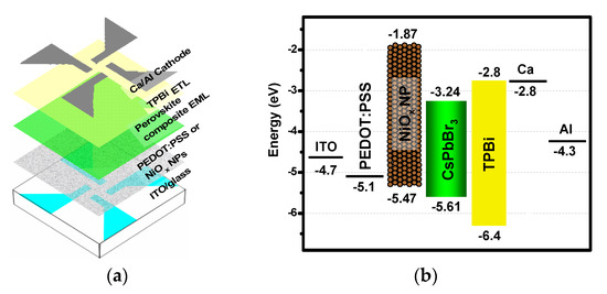
Figure 1.
(a) Schematic PeLED architecture and (b) corresponding energy band diagram with an alternative hole transport layer (HTL), poly (3,4-ethylenedioxythiophene): poly (styrenesulfonate) (PEDOT:PSS), or NiOx nanoparticles (NPs).
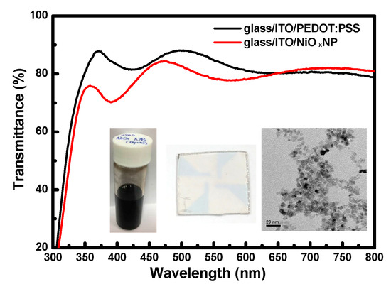
Figure 2.
Transmittance spectra of PEDOT:PSS and colloidal NiOx NPs spin-coated on the ITO-glass substrates. Insets from left to right show the photographs of NiOx NP ink and thereby a spin-coated film and the TEM image of NPs.

Table 1.
Different HTLs and recipes of precursor solution for EML in perovskite LEDs (PeLEDs).
2.3. Characterizations
As for the thin film and device characterization, the X-ray diffraction (XRD) pattern was obtained using a Rigaku MiniFlex II X-ray diffractometer. The absorption and electroluminescence (EL) spectra were measured by the UV-VIS spectrometer (LINKO, LKU-5200) and a fiber-optic spectrometer (Ocean Optics, USB 4000), respectively. The size of nanoparticles, surface morphology of films, and UPS spectra were obtained using a transmission electron microscope (TEM) (JEOL, JEM-2100F), an atomic force microscope (AFM) (Bruker, Innova), and an electron spectrometer (Chigasaki, ULVAC-PHI), respectively. Current–voltage (I–V) curves of the PeLEDs were measured using a Keithley 2400 source meter. Moreover, the luminance properties under various voltages were obtained by calibrating the photocurrent of a silicon detector using a luminance meter (Minolta, LS-110).
3. Results and Discussion
In Figure 2, the transmittance of NiOx NP layer is slightly lower than that of PEDOT:PSS in the visible light region, respectively. The overall transmittance at 520 nm was larger than 80% for both of the films coated on ITO-glass. The XRD patterns of the spin-coated EML from the Solution-A with and without the organic additives are shown in Figure 3. Basically, all the patterns are dominated by the peaks corresponding to orthorhombic CsPbBr3 polycrystals. In the EML coated with only Solution A, the pattern was dominant by the (220) diffraction peak, the same as that of the CsPbBr3 powder. However, by comparing the variation of the main peaks of the doped films, it is evident that the addition of PEO and FIrpic was especially favorable for the grain growth along the [110] direction. The decrease of intensity related to the (220) peak in the EML additionally doped with FIrpic can be possibly attributed to the variation of lateral grain size (see Figure 4h). Moreover, it was also revealed that FIrpic could definitely suppress the grain growth of (020) phase. By adding the TPBi, a new diffraction peak was shown at ~31.6°. This peak should not be related to the formation of 2-D CsPb2Br5 or 0-D Cs4PbBr6 crystals [25]. Nonetheless, the real attribution is still under investigation. No diffraction signals associated with PEO, TPBi, and FIrpic were detected.
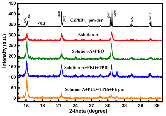
Figure 3.
XRD patterns of EMLs derived from various precursor solutions.
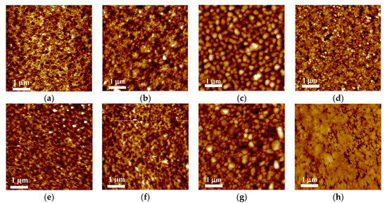
Figure 4.
AFM images of (a) PEDOT:PSS, (b) NiOx NP HTLs, and the EML of (c) Device-PA, (d) Device-PB, (e) Device-PC, (f) Device-PD, (g) Device-NA, and (h) Device-ND.
The comparison of surface morphology of each spin-coated layer is shown in Figure 4. Through calculation, the value of rms surface roughness (Rq) was 2.0, 5.7, 10.5, 8.4, 5.1, 4.8, 15.3 and 5.5 nm, respectively. It can be seen that the PEDOT:PSS (Rq = 2.0 nm) was homogeneous and flat whereas the NiOx NP layer was slightly rough (Rq = 5.7 nm) owing to the aggregation of NPs (inset of Figure 2). The surface of pure CsPbBr3 film on PEDOT:PSS or NiOx NP layer was quite rough (Rq > 10 nm), with distinct and diverse-sized 3-D CsPbBr3 crystal grains separated by clear boundaries. As shown in Figure 4d, the addition of PEO reduced the film roughness by reducing the grain size and shrinking the size distribution [25,26]. It was found that Rq could be further decreased by adding more PEO. Too much of the electrically resistive PEO, however, was not beneficial for device performance [27]. In Figure 4e,f, the influence of TPBi and FIrpic on CsPbBr3 films was very different to that of PEO. When TPBi is added, the original small grains in Figure 4d tend to interconnect with one another, becoming a 2-D crystal network, which was enhanced by adding FIrpic. In Figure 4h the additive-assisted CsPbBr3 film on NiOx NPs, the CsPbBr3 crystals coalesced and became large and flat grains with few voids.
In PeLED characterization, the luminance–current density–voltage (L–J–V) and the current efficiency–current density curves are shown in Figure 5a. For Device-PA and Device-NA with pure CsPbBr3 EML, the leakage current at 0~2.4 V was remarkably high because of the rough EML surface with plenty of pinholes, which acted as the shunt pathway. Furthermore, the large difference between the turn-on voltages for current injection (~2.5 V) and light threshold (VT~3.5 V) in Device-PA indicates that the injection charges were extremely unbalanced, while the defective CsPbBr3 crystals led to very low luminance. The clear trend of current efficiency (ηCE) increasing with current density shown in Figure 5b for Device-PA is strong evidence of the competition between leakage and injection current.
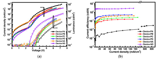
Figure 5.
(a) L–J–V and (b) current efficiency-current density (ηCE-J) characteristics of the PeLEDs.
For Device-PB, Device-PC, and Device-PD, the crystal quality of EML was improved by reducing the roughness and eliminating the defects, which caused lower VT and higher luminance. In circumstances of neglectable leakage current, the higher current efficiency in Device-PD exhibited higher radiative recombination rate of excitons in the EML, probably owing to the phosphorescent capability of FIrpic for efficient Förster energy transfer [28].
Furthermore, Device-ND achieved the low light threshold voltage VT of 2.4 V, high luminance maximum (Lmax) of 4456 cd/m2, and high current efficiency of 2.9 cd/A by adopting the NiOx NPs and the additive-assisted EML that gave a better hole transporting and high radiative recombination rate, respectively. It can be clearly observed that the threshold of the minority carrier (holes) injection at 2.4 V and the onset of majority carrier (electrons) injection at ~2.3 V matched pretty well, which suggests that those negative effects such as Auger recombination (trions) and improper shift of exciton recombination zone can therefore be prevented [29,30]. Overall, compared with Device-PA, Device-ND had roughly 17- and 94-fold increased Lmax and ηCE, respectively.
Finally, the normalized EL spectra of Device-PB, Device-NA, and Device-ND are shown in Figure 6 for observing the effect of organic additives on the emission of perovskite crystals. The spectrum of Device-PA is not shown because of the low EL intensity, while the spectra of Device-PC and Device-PD are very similar to that of Device-ND. No emission from the TPBi or FIrpic was detected, possibly due to their low doping concentration, low emission efficiency, and exciton energy transfer just mentioned [28]. However, the spectra are slightly different in peak position. By adding the additives, the peak position of the green light was shifted from 521.7 (Device-NA) to 519.5 nm (Device-ND), with no obvious change in spectral width (~17 nm). Also, the spectrum of Device-PB was broadened to 18.3 nm.
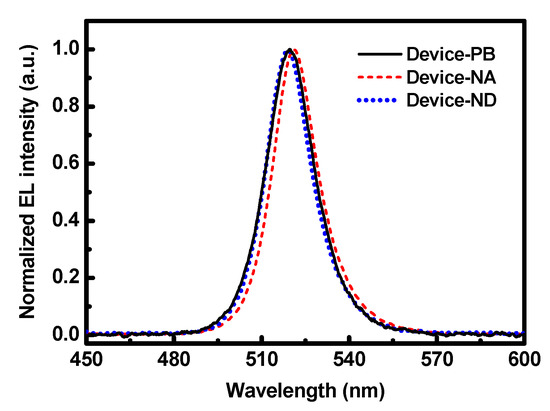
Figure 6.
Normalized EL spectra of Device-PB, Device-NA, and Device-ND.
4. Conclusions
In conclusion, the fabrication and characterization of an ambient-processed, electrically driven PeLED with a multiple-additive-assisted CsPbBr3 EML and a colloidal NiOx NP HTL were demonstrated. From the experimental results, it can be understood that the deeper VBM (−5.47 eV) of 5 nm-sized NiOx NPs facilitated the injection of holes, the minority carrier, into EML by decreasing the energy barrier without sacrificing the transmittance of the HTL. The doping of PEO was significantly beneficial to reduce the roughness of EML and thus reduce the device leakage current, whereas TPBi and FIrpic helped to improve the crystal quality by interconnecting the adjacent crystal grains to reduce the PL-inefficient boundaries. In terms of the crystal orientation, additives tended to favor the grain growth along the [110] direction. Because of the improved crystal quality of the spin-coated perovskite film and fairly balanced charge injection, the novel PeLED turned on at a very low voltage of 2.4 V, and exhibited a high luminance maximum of 4456 cd/m2 and an enhanced current efficiency of 2.9 cd/A, which is about 17- and 94-fold of that of the PeLED with a pure/untreated CsPbBr3 EML and a conventional PEDOT:PSS HTL.
Supplementary Materials
The following are available online at https://www.mdpi.com/2079-6412/10/4/336/s1, Figure S1, Absorption and photoluminescence (PL) spectra of the synthesized CsPbBr3 powder. Insets are the photographs of CsPbBr3 powder under white and UV light irradiation, respectively; Figure S2, UPS spectra of the NiOx NP HTL. According to the cutoff values, the valence band maximum (Ev) of NiOx NP HTL can be determined as 5.47 eV.
Author Contributions
Conceptualization, Methodology and Writing—Original Draft Preparation, C.-Y.H.; Writing—Review and Editing, S.-P.C. and A.G.A.; Supervision, Z.-H.W.; Conceptualization and Methodology, C.-C.Y. All authors have read and agreed to the published version of the manuscript.
Funding
This research was funded by the Ministry of Science and Technology of the Republic of China under grant number 108-2221-E-143-005-MY2.
Conflicts of Interest
The authors declare no conflict of interest.
References
- Lin, Y.H.; Pattanasattayavong, P.; Anthopoulos, T.D. Metal-halide perovskite transistors for printed electronics: Challenges and opportunities. Adv. Mater. 2017, 29, 1702838. [Google Scholar]
- Zhang, X.; Liu, H.; Wang, W.; Zhang, J.; Xu, B.; Karen, K.L.; Zheng, Y.; Liu, S.; Chen, S.; Wang, K.; et al. Hybrid perovskite light-emitting diodes based on perovskite nanocrystals with organic–inorganic mixed cations. Adv. Mater. 2017, 29, 1606405. [Google Scholar]
- Yang, J.M.; Luo, Y.; Bao, Q.; Li, Y.Q.; Tang, J.X. Recent advances in energetics and stability of metal halide perovskites for optoelectronic applications. Adv. Mater. Interfaces 2018, 6, 1801351. [Google Scholar]
- Gong, X.; Huang, Z.; Sabatini, R.; Tan, C.S.; Bappi, G.; Walters, G.; Proppe, A.; Saidaminov, M.I.; Voznyy, O.; Kelley, S.O.; et al. Contactless measurements of photocarrier transport properties in perovskite single crystals. Nat. Commun. 2019, 10, 1591. [Google Scholar]
- Chen, Z.; Turedi, B.; Alsalloum, A.Y.; Yang, C.; Zheng, X.; Gereige, I.; Alsaggaf, A.; Mohammed, O.F.; Bakr, O.M. Single-crystal MAPbI3 perovskite solar cells exceeding 21% power conversion efficiency. ACS Energy Lett. 2019, 4, 1258–1259. [Google Scholar] [CrossRef]
- Huang, C.Y.; Huang, S.J.; Liu, M.H.M. Hybridization of CsPbBr1.5I1.5 perovskite quantum dots with 9,9-dihexylfluorene co-oligomer for white electroluminescence. Org. Electron. 2017, 44, 6–10. [Google Scholar]
- Wang, X.; Lu, G.; Zhang, M.; Gao, Y.; Liu, Y.; Zhou, L.; Lin, Z. High performance planar structure perovskite solar cells using a solvent dripping treatment on hole transporting layer. Coatings 2020, 10, 127. [Google Scholar] [CrossRef]
- Huang, C.Y.; Wu, C.C.; Wu, C.L.; Lin, C.W. CsPbBr3 perovskite powder, a robust and mass-producible single-source precursor: Synthesis, characterization, and optoelectronic applications. ACS Omega 2019, 4, 8081–8086. [Google Scholar]
- Kulbak, M.; Gupta, S.; Kedem, N.; Levine, I.; Bendikov, T.; Hodes, G.; Cahen, D. Cesium enhances long-term stability of lead bromide perovskite-based solar cells. J. Phys. Chem. Lett. 2016, 7, 167–172. [Google Scholar]
- Chen, M.; Ju, M.G.; Garces, H.F.; Carl, A.D.; Ono, L.K.; Hawash, Z.; Zhang, Y.; Shen, T.; Qi, Y.; Grimm, R.L.; et al. Highly stable and efficient all-inorganic lead-free perovskite solar cells with native-oxide passivation. Nat. Commun. 2019, 10, 16. [Google Scholar]
- Jeon, N.J.; Na, H.; Jung, E.H.; Yang, T.Y.; Lee, Y.G.; Kim, G.; Shin, H.W.; Seok, S.I.; Lee, J.; Seo, J. A fluorene-terminated hole-transporting material for highly efficient and stable perovskite solar cells. Nature Energy. Nat. Energy 2018, 3, 682–689. [Google Scholar]
- Jin, F.; Zhao, B.; Chu, B.; Zhao, H.; Su, Z.; Li, W.; Zhu, F. Morphology control towards bright and stable inorganic halide perovskite light-emitting diodes. J. Mater. Chem. C 2018, 6, 1573–1578. [Google Scholar] [CrossRef]
- Cheng, L.; Cao, Y.; Ge, R.; Wei, Y.Q.; Wang, N.N.; Wang, J.P.; Huang, W. Sky-blue perovskite light-emitting diodes based on quasi-two-dimensional layered perovskites. Chin. Chem. Lett. 2017, 28, 29–31. [Google Scholar] [CrossRef]
- Tao, S.; Schmidt, I.; Brocks, G.; Jiang, J.; Tranca, I.; Meerholz, K.; Olthof, S. Absolute energy level positions in tin-and lead-based halide perovskites. Nat. Commun. 2019, 10, 2560. [Google Scholar]
- Cho, H.; Jeong, S.H.; Park, M.H.; Kim, Y.H.; Wolf, C.; Lee, C.L.; Heo, J.H.; Sadhanala, A.; Myoung, N.; Yoo, S.; et al. Overcoming the electroluminescence efficiency limitations of perovskite light-emitting diodes. Science 2015, 350, 1223–1225. [Google Scholar] [CrossRef]
- Chih, Y.K.; Wang, J.C.; Yang, R.T.; Liu, C.C.; Chang, Y.C.; Fu, Y.S.; Lai, W.C.; Chen, P.; Wen, T.C.; Huang, Y.C.; et al. NiOx electrode interlayer and CH3NH2/CH3NH3PbBr3 interface treatment to markedly advance hybrid perovskite-based light-emitting diodes. Adv. Mater. 2016, 28, 8687–8694. [Google Scholar]
- Chen, L.C.; Lee, K.L.; Huang, C.Y.; Lin, J.C.; Tseng, Z.L. Preparation and characteristics of MAPbBr3 perovskite quantum dots on NiOx film and application for high transparent solar cells. Micromachines 2018, 9, 205. [Google Scholar]
- Huang, C.Y.; Cheng, C.Y.; Shih, Y.S. All-solution-processed fluorene/dibenzothiophene-S,S-dioxide blue co-oligomer light-emitting diodes with an electron transporting PEI/ultrafine-ZnO-nanoparticle bilayer. RSC Adv. 2017, 7, 41855–41861. [Google Scholar] [CrossRef]
- Vu, H.T.; Su, Y.K.; Chiang, R.K.; Huang, C.Y.; Chen, C.J.; Yu, H.C. Solution-processable MoOx for efficient light-emitting diodes based on giant quantum dots. IEEE Photon. Technol. Lett. 2016, 28, 2156–2159. [Google Scholar]
- Huang, C.Y.; Lai, J.H. Efficient polymer light-emitting diodes with ZnO nanoparticles and interpretation of observed sub-bandgap turn-on phenomenon. Org. Electron. 2016, 32, 244–249. [Google Scholar] [CrossRef]
- Huang, C.Y.; Yang, C.C.; Yu, H.C.; Chen, Y.C. Impact of preparation condition of ZnO electron transport layer on performance of hybrid organic-inorganic light-emitting diodes. J. Appl. Phys. 2014, 115, 083109. [Google Scholar]
- Danial, A.S.; Awad, M.I.; Al-Odail, F.A.; Saleh, M.M. Effect of different synthesis routes on the electrocatalytic properties of NiOx nanoparticles. J. Mol. Liquids 2017, 225, 919–925. [Google Scholar] [CrossRef]
- Cho, H.; Wolf, C.; Kim, J.S.; Yun, H.J.; Bae, J.S.; Kim, H.; Heo, J.M.; Ahn, S.; Lee, T.W. High-efficiency solution-processed inorganic metal halide perovskite light-emitting diodes. Adv. Mater. 2017, 29, 1700579. [Google Scholar] [CrossRef]
- Zhang, H.; Cheng, J.; Lin, F.; He, H.; Mao, J.; Wong, K.S.; Jen, A.K.Y.; Choy, W.C.H. Pinhole-free and surface-nanostructured NiOx film by room-temperature solution process for high-performance flexible perovskite solar cells with good stability and reproducibility. ACS Nano 2016, 10, 1503–1511. [Google Scholar] [CrossRef] [PubMed]
- Palazon, F.; Dogan, S.; Marras, S.; Locardi, F.; Nelli, I.; Rastogi, P.; Ferretti, M.; Prato, M.; Krahne, R.; Manna, L. From CsPbBr3 nano-inks to sintered CsPbBr3−CsPb2Br5 films via thermal annealing: Implications on optoelectronic properties. J. Phys. Chem. C 2017, 121, 11956–11961. [Google Scholar]
- Yang, X.; Gu, H.; Li, S.; Li, J.; Shi, H.; Zhang, J.; Liu, N.; Liao, Z.; Xu, W.; Tan, Y. Improved photoelectric performance of all-inorganic perovskite through different additives for green light-emitting diodes. RSC Adv. 2019, 9, 34506–34511. [Google Scholar]
- Wu, C.; Zou, Y.; Wu, T.; Ban, M.; Pecunia, V.; Han, Y.; Liu, Q.; Song, T.; Duhm, S.; Sun, B. Improved performance and stability of all-inorganic perovskite light-emitting diodes by antisolvent vapor treatment. Adv. Func. Mater. 2017, 27, 1700338. [Google Scholar] [CrossRef]
- Gao, C.H.; Ma, X.J.; Zhang, Y.; Yu, F.X.; Xiong, Z.Y.; Wang, Z.Q.; Wang, R.; Jia, Y.L.; Zhou, D.Y.; Xiong, Z.H. 84% efficiency improvement in all-inorganicperovskite light-emitting diodes assisted by a phosphorescent material. RSC Adv. 2018, 8, 15698–15702. [Google Scholar] [CrossRef]
- Maggiore, A.; Pugliese, M.; Maria, F.D.; Accorsi, G.; Gazzano, M.; Fabiano, E.; Tasco, V.; Esposito, M.; Cuscunà, M.; Blasi, L.; et al. Exploiting photo- and electroluminescence properties of FIrpic organic crystals. Inorg. Chem. 2016, 55, 6532–6538. [Google Scholar] [CrossRef] [PubMed]
- Li, Y.; Ding, T.; Luo, X.; Chen, Z.; Liu, X.; Lu, X.; Wu, K. Biexciton Auger recombination in mono-dispersed, quantum-confined CsPbBr3 perovskite nanocrystals obeys universal volume-scaling. Nano Res. 2019, 12, 619–623. [Google Scholar]
© 2020 by the authors. Licensee MDPI, Basel, Switzerland. This article is an open access article distributed under the terms and conditions of the Creative Commons Attribution (CC BY) license (http://creativecommons.org/licenses/by/4.0/).