Article

Trap State and Charge Recombination in Nanocrystalline Passivized Conductive and Photoelectrode Interface of Dye-Sensitized Solar Cell

by
Siti Nur Azella Zaine
1,2,*,
Norani Muti Mohamed
1,2,
Mehboob Khatani
3,
Adel Eskandar Samsudin
3 and
Muhammad Umair Shahid
1
1
Fundamental and Applied Science Department, Universiti Teknologi PETRONAS, 32610 Seri Iskandar, Perak, Malaysia
2
Centre of Innovative Nanostructures and Nanodevices (COINN), Universiti Teknologi PETRONAS, 32610 Seri Iskandar, Perak, Malaysia
3
Electrical and Electronic Department, Universiti Teknologi PETRONAS, 32610 Seri Iskandar, Perak, Malaysia
*
Author to whom correspondence should be addressed.
Coatings 2020, 10(3), 284; https://doi.org/10.3390/coatings10030284
Submission received: 3 January 2020 / Revised: 27 January 2020 / Accepted: 29 January 2020 / Published: 19 March 2020
(This article belongs to the Special Issue Coatings for Solar Cell Applications)

Abstract

:
The dynamic competition between electron generation and recombination was found to be a bottleneck restricting the development of high-performance dye-sensitized solar cells (DSSCs). Introducing a passivation layer on the surface of the TiO2 photoelectrode material plays a crucial role in separating the charge by preventing the recombination of photogenerated electrons with the oxidized species. This study aims to understand in detail the kinetics of the electron recombination process of a DSSC fabricated with a conductive substrate and photoelectrode film, both passivized with a layer of nanocrystalline TiO2. Interestingly, the coating, which acted as a passivation layer, suppressed the back-electron transfer and improved the overall performance of the integrated DSSC. The passivation layer reduced the exposed site of the fluorine-doped tin oxide (FTO)–electrolyte interface, thereby reducing the dark current phenomenon. In addition, the presence of the passivation layer reduced the rate of electron recombination related to the surface state recombination, as well as the trapping/de-trapping phenomenon. The photovoltaic properties of the nanocrystalline-coated DSSC, such as short-circuit current, open-circuit voltage, and fill factor, showed significant improvement compared to the un-coated photoelectrode film. The overall performance efficiency improved by about 22% compared to the un-coated photoelectrode-based DSSC.

1. Introduction

A dye-sensitized solar cell (DSSC), also known as a Gratzel cell, displays artificial photosynthesis, where a dye analogous to chlorophyll absorbing light generates electrons which enter the conduction band of a high-surface-area semiconductor film and travel along an external circuit, producing electricity [1,2,3,4]. Unlike conventional PV, DSSC has a better charge separation, where the dye is responsible for the absorption of radiation and transportation of carriers through the semiconductor oxide in the form of titanium dioxide. The basic structure of a DSSC comprises a layer of photoelectrode material, photosensitized by a monolayer of dye, assembled between a sandwich layer of transparent electrically conducting substrate and conducting catalytic substrate. An electrolyte based on an iodide/tri-iodide redox system is filled between the layer gap of photosensitized titania and transparent electrically conducting catalytic substrate.
The mesoporous oxide photoelectrode material is the heart of a DSSC. It has responsibilities in anchoring the molecules of the dye sensitizer, and it acts as a medium for the transportation of electrons. In recent years, the development of binary and ternary oxide nanostructured photoelectrode materials such as titanium dioxide (TiO2), zinc oxide (ZnO), tin oxide (SnO2), and zinc tin oxide (Zn2SnO4) attracted great attention due to their suitable conduction band and unique characteristics for DSC application. As of now, TiO2 is the semiconductor of choice due to its promising properties such as wide bandgap energy, low cost, abundance, and non-toxic oxides. Moreover, the chemical inertness of TiO2 makes it possible to allow the dye sensitizer molecule, which commonly has a carboxylate anchoring group, to be attached to the photoelectrode surface. Additionally, other distinguishing features of TiO2 such as the high relative permittivity of anatase (~30–40) helps in lowering the electrostatic interaction between the injected electrons and oxidized dye molecules, thus reducing the possibilities of electron recombination [5]. Anatase (Eg = 3.23 eV), rutile (Eg = 3.05 eV), and brookite (Eg = 3.26 eV) are three crystalline TiO2 polymorphs that naturally exist. Brookite with an orthorhombic structure is difficult to synthesize in the laboratory compared to anatase and rutile. Even though rutile and anatase have the same tetragonal structure, a higher Fermi level of anatase by 0.1 eV compared to rutile makes it more desirable for DSSC application [6].
When the photosensitized dye receives enough energy from the incident photons, dye molecules transform into the excited state and rapidly release electrons. The electrons are injected into the conduction band of the TiO2, leaving the dye in the oxidized state while holes are released by the reduction and oxidation process taking place in the electrolyte. Due to comparatively slow electron transport through the mesoporous network, the injected electrons are stimulated to travel in the reverse direction and recombine with the tri-iodide species in the electrolyte. This process is known as dark current and typically occurs on the order of milliseconds to seconds [1,2,3,4,5,6,7]. Furthermore, the presence of massive injected electrons might promote the electrons to recombine with the oxidized dye molecules, in which the process usually happens in the range of micro- to milliseconds [1,2,3,4,5,6,7]. These recombination processes occur at the TiO2–dye–electrolyte interface with their probability determined by the kinetics recombination reaction.
Several strategies were introduced to suppress the charge recombination process, for instance, the introduction of metal and/or non-metal element doping [8,9,10,11,12,13,14,15,16,17], as well as metal oxide coatings [18,19,20,21,22,23], as a passivation or blocking layer. The substitution of Ti4+ with a different cationic dopant (typically metal-type dopant) modifies the conduction band, while replacing the O2− with different anions affects the valence band of TiO2. The dopant, usually chosen based on the atomic radius, must not differ too much from the desired ions to be replaced in order to avoid lattice distortion, which would induce new defects that can hamper the performance of the fabricated DSSC. However, various metal and non-metal dopants were explored [24] in order to understand the effect of doping on the mechanism of electron transfer in DSSCs. Since the dye molecules are anchored to the Ti atoms, the replacement of Ti with other cations usually affects the amount of anchored dye due to the different binding strength between the dye molecules and the newly introduced cation elements.
Several metal oxides were explored as potential passivation layers for DSSC application. These include Al2O3 [25], SnO2 [26], TiO2 [27,28,29,30,31,32,33,34], and graphene/reduced graphene oxide [35,36,37,38,39,40]. The potential of a tin oxide (SnO2) thin film as the passivation layer was reported by Kim et al. [26]. In their study, an ultrathin layer of SnO2 was deposited onto a fluorine-doped tin oxide (FTO) substrate through layer-by-layer deposition of SnO2 nanoparticles. The idea was to create a cascade energy band since the conduction band of SnO2 is lower compared to TiO2 but higher compared to bulk FTO. However, due to the low electron mobility of SnO2, the passivation layer with a thickness of more than 10 nm prevented electron diffusion, thus promoting the recombination process.
Recently, graphene oxide and reduced graphene oxide films were also explored as passivation layers due to their exceptional electronic and optical properties [35,36,37,38,39,40]. The first reduced graphene oxide passivation layer was reported by Kim et al. [40] with the idea that it could provide a barrier between the FTO substrate and electrolyte. In addition, the process also required low-temperature deposition without utilizing hazardous chemicals. Even though their approach showed improvement in the overall performance efficiency, the capability of the passivation film to absorb light and act as a catalyst for the reduction of tri-iodide did not seem to be more beneficial compared to other metal oxides as passivation layers. On the other hand, Chen et al. introduced a thin layer of thermally reduced graphene oxide (TRGO) as a passivation layer, resulting in better performance efficiency of the DSSC due to an increment in the photocurrent [36]. The TRGO coated through a spin coating process also showed less light absorption, resulting in an optimum photon radiance striking the dye molecules, thus helping to produce an optimum number of excited electrons. Since graphene oxide has potential in reducing the recombination of electrons while becoming an insulating barrier, a very thin layer of graphene oxide which is enough for tunneling is preferred. However, the implementation of graphene oxide as a passivation layer is unfavorable in the case where it is highly active for the redox mediator, such as when a cobalt bipyridine redox couple was used as an electrolyte [35].
Nanocrystalline TiO2 as a passivation layer was proven to contribute to the improvement of inter-particle connectivity, increase surface area for anchoring dye molecules, and create an electron barrier on the surface of photoelectrode material, thereby facilitating more electron generation and accelerating electron transport [21,22,23,24,25,27,28,29]. However, relatively little attention was paid to the trap state and charge transport properties of the fabricated DSSC coated with nanocrystalline TiO2 on the FTO substrate, as well as photoelectrode films as passivation layers. Here, we report on the effect of a conductive substrate and TiO2 photoelectrode film, both coated with nanocrystalline TiO2, on the electrochemical properties, emphasizing the trap state and electron recombination of the fabricated DSSC. The outcome was discussed in detail based on electrochemical impedance spectroscopy and open-circuit voltage decay analysis. The objective of this study was not to achieve the highest efficiency of DSSC, but rather to acquire a better understanding of the electrochemical process, which is important for the development of an effective passivation layer in high-performance DSSCs.

2. Materials and Methods

In preparing the photoelectrode paste, TiO2 nanoparticles as the active photoelectrode material, ultra-filtered deionized water, ethanol absolute, acetic acid, terpineol, ethyl cellulose #46070 (viscosity: 5–15 mPa∙s, 5% in toluene/ethanol 80:20 at 25 °C, Fluka), and ethyl cellulose #46080 (viscosity: 530–70 mPa∙s, 5% in toluene/ethanol 80:20 at 25 °C, Fluka) were used. The photoelectrode paste was prepared according to the method introduced by Ito et al. [41].
The precursor solution for nanocrystalline coating was prepared using titanium(IV) chloride (TiCl4). The as-received TiCl4 was mixed with pre-frosted deionized water in an ice bath to produce a precursor solution of 2 M TiCl4. Prior to use, the precursor solution was diluted to 40 mM using deionized water. The diluted TiCl4 solution was used in the dip-coating process to deposit the nanocrystalline TiO2 passivation layer. The coating process was done at 70 °C in an oven for 30 min. The coated samples were then rinsed with deionized water and ethanol solution. The sample coated with a nanocrystalline layer on the FTO substrate is denoted as BL, the sample coated with a nanocrystalline layer on the FTO and after deposition of the first layer of the photoelectrode is denoted as BML, and the sample coated with a nanocrystalline layer on the FTO and after deposition of the second layer of the photoelectrode is denoted as BTL. A sample without nanocrystalline coating was also prepared as a control. By using a screen-printing mesh of 43T (threads per cm), the total thickness of the prepared photoelectrode samples was controlled to be about 12 µm (about 6 µm for each printed photoelectrode layer). Figure 1 illustrates the configuration of the prepared samples. The FTO substrates before and after printing with the photoelectrode film were heat-treated at 500 °C to remove the constituents and organic binders.
The prepared working electrodes were then immersed into 0.25 mM N719 dye in ethanol solution and kept at room temperature overnight to complete the sensitizer uptake. Then, the working electrodes were rinsed with anhydrous alcohol to remove any non-bonded dye which may interfere with DSSC performance. Both working and counter electrodes were assembled into a sandwich layer and sealed with a hot-melt thermoplastic gasket. An electrolyte solution of an iodide/tri-iodide redox couple solution was then injected through a hole drilled on the platinized counter electrode. The fabricated DSSCs had an active area of 1 cm2. Figure 2 shows the schematic diagram and the optical images of the fabricated DSSC.
An assessment of the surface morphology of uncoated and nanocrystalline-coated FTO substrate, as well as the printed photoelectrode film, was obtained using a Zeiss Supra 55VP field-emission scanning electron microscope (FESEM), run with an accelerating voltage of 5.0 kV. Energy-dispersive X-ray spectroscopy (EDX) attached to the FE-SEM unit was used for element mapping. The phase presence after coating was further verified using a powder X-ray diffractometer (XRD, Model: X’Pert3 Powder, PANalytical). The XRD analysis was operated at 40 kV using an Ni-filtered Cu Kα radiation (λ = 1.54 Å) with a step scan size of 0.02°/step and an exposure time of 3 s/step in the range 2θ of 10° to 80°. UV–Vis analysis of the desorbed dye solution was tested using UV–Vis spectroscopy (Cary 100, Agilent) to study the capability of the photoelectrode films in absorbing dye molecules.
The spectra of electrochemical impedance spectroscopy (EIS) were recorded using Gamry Instruments PCI4-300 operating in two-electrode mode. The analysis was carried out in the dark at various forward bias voltages in the 300 kHz to 0.1 Hz frequency range and an alternating current (AC) modulation signal of 10 mV. Echem Analyst software was used to fit the frequency-dependent impedance. For the open-circuit voltage decay study, the fabricated cells were first irradiated with AM 1.5 solar light for 5 s to a steady voltage. The illumination was then turned off, and the open-circuit voltage decay was recorded using EIS for an interval of 0.5 s over a period of 120 s. The performance of the integrated cells was established using a Universal Photovoltaic Test System under 100 mW/cm2 intensity of an illuminant Xenon lamp at an AM 1.5 radiation angle connected to a voltmeter and ampere meter (Model 2420, Keithly) with variable load.

3. Results

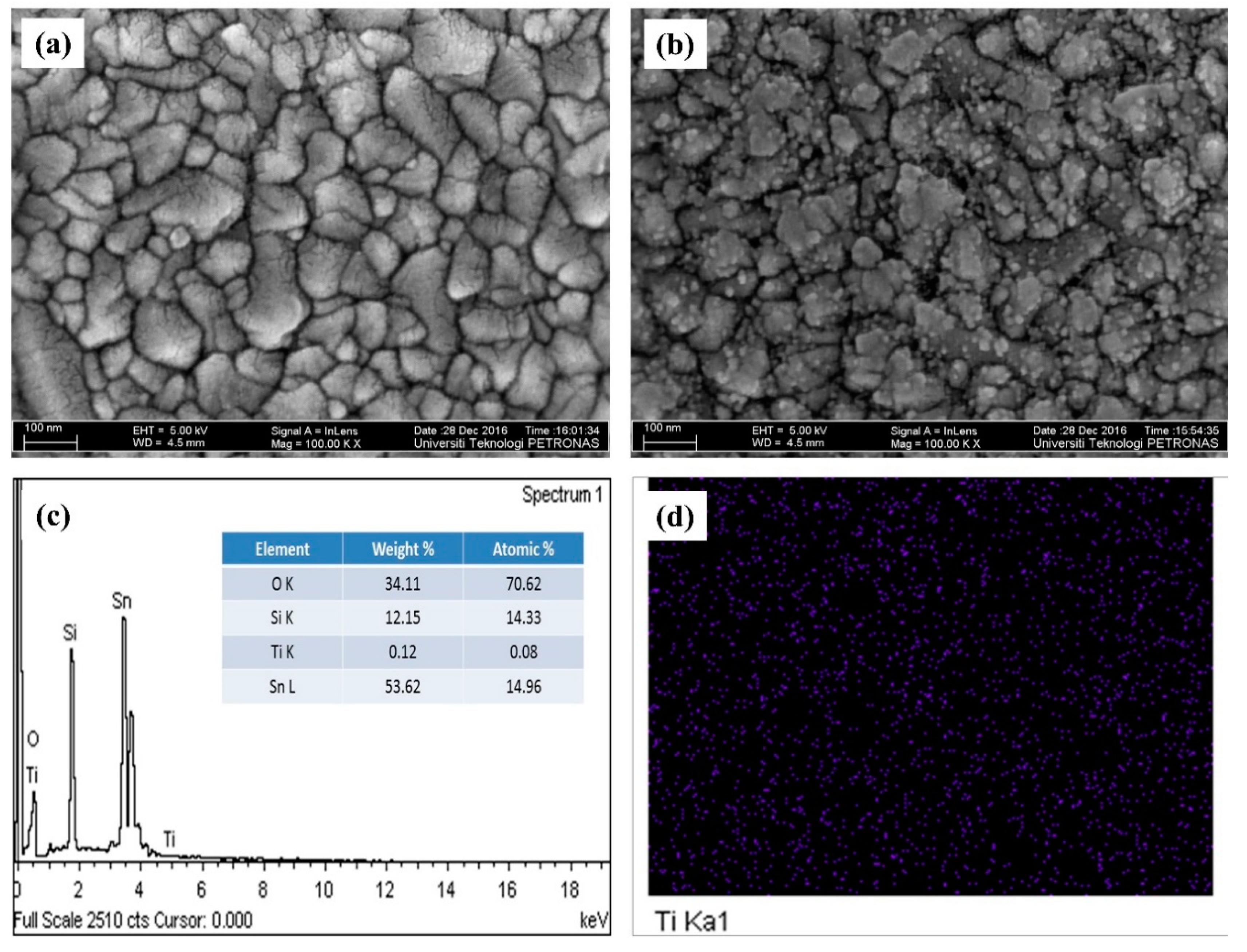
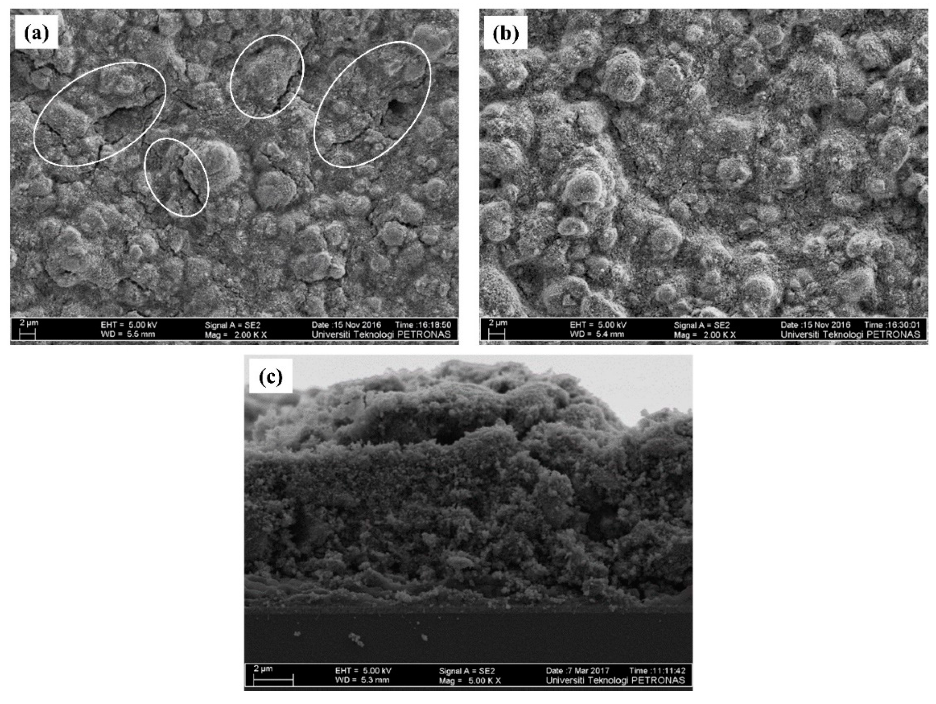
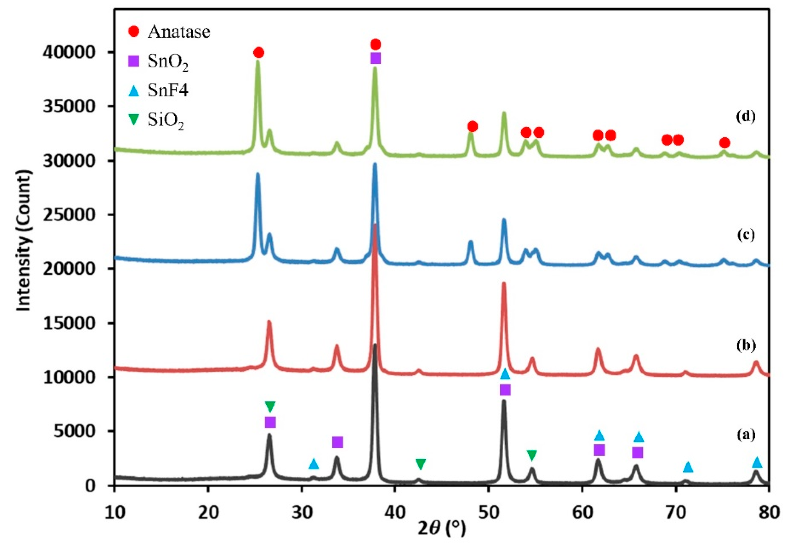
3.1. Morphology and Microstructure of Photoelectrode Film

The morphology of nanocrystalline-coated FTO and photoelectrode films was examined using FE-SEM analysis. Figure 3a,b show the FE-SEM images of the top view of the FTO substrate before and after being coated with nanocrystalline TiO2, respectively. The images taken at a magnification of 100,000× reveal that the surface of the FTO substrate was rough with a uniform arrangement of crystalline tin oxide. After the coating process, the FTO surface substrate was covered with a layer of nanocrystalline TiO2. The nanocrystalline TiO2 was in the form of irregular particles with a size of less than 10 nm. Further analysis with EDX (Figure 3c) confirmed the presence of the Ti element, which contributed about 0.08 at.% of the total elements. The presence of Ti and O peaks can be obviously found in the EDX spectra, indicating the presence of TiO2 without the impurities of chlorine contributed from the precursor. The presence of Si (14.33 at.%) and Sn (14.96 at.%) was contributed by the FTO elements on the surface of the glass substrate. The element mapping was taken at 100,000× magnification of the coated FTO substrate (Figure 3d), clearly showing that the Ti element was well distributed on the surface of FTO, signifying a successful uniform coating process of the nanocrystalline TiO2 layer.
The FE-SEM analysis was also utilized in order to analyze the effect of the nanocrystalline coating on the morphology of the photoelectrode layer. The results of the analysis are shown in Figure 4. The FE-SEM image of the top view of the uncoated photoelectrode film layer, taken at a magnification of 2000× clearly shows the presence of surface cracks up to a few micrometers long (Figure 4a). The nanocrystalline coating helped to improve film cracking, with no clear surface crack seen through FE-SEM analysis at 2000× magnification, as evidenced in Figure 4b. The improvement of the deposited material was due to the formation of nanocrystalline TiO2 by the coating process, which filled the gaps between the nanoparticles, thus improving the connectivity and reducing film cracking. Figure 4c confirms that the photoelectrode film exhibited a thickness of about 12 µm with no presence of boundaries between the deposited layers. This condition was important in order to avoid the influence of film imprecision on the analysis. The presence of boundaries between photoelectrode layers would result in increased electron transport resistance, thereby increasing the possibilities of electron recombination and, thus, contributing to the low performance of the fabricated DSSC.
Figure 5 shows the XRD spectrum of the FTO substrate and TiO2 photoelectrode films before and after being coated with nanocrystalline TiO2. Figure 5a clearly shows that the FTO substrate exhibited peaks at about 26.5°, 33. 7°, 37.8°, 51.5°, 61.6°, and 65.6°, corresponding to the tin oxide phase (PDF 00-046-1088), as well as peaks at 31.2°, 51.5°, 61.6°, 65.6°, 70.9°, and 78.5° corresponding to the tin fluoride (PDF 01-085-2126) phase, and peaks at about 26.5°, 42.4°, and 54.6° corresponding to the silicon dioxide phase (PDF 01-089-8937). The presence of these phases matched well with the properties of the fluorine-doped tin oxide (FTO) glass substrate. The XRD spectra of the nanocrystalline-coated FTO substrate showed no additional diffraction peaks compared to the bare FTO substrate, which would represent the presence of nanocrystalline TiO2, due to the deposition of a very thin layer of nanocrystalline TiO2. On the other hand, the FTO substrate printed with photoelectrode TiO2 showed Miller indices corresponding to the presence of the anatase structure of (101) at 25.3°, (004) at 37.8°, (200) at 48.1°, (105) at 53.9°, (211) at 55.1°, (213) at 62.1°, (204) at 62.7°, (116) at 68.7°, (220) at 70.3°, and (215) at 75.0°. The FTO peaks exhibited a noticeable decrease in the intensity after deposition of TiO2 due to the thick layer of TiO2 photoelectrode film, which weakened the XRD signal of the FTO glass. However, comparing the intensity of the (101) peak at 25.3°, the nanocrystalline-coated film exhibited a higher peak (9157 a.u.) compared to the uncoated film (8798 a.u.). This result suggests that the process of nanocrystalline coating helped to improve the crystallinity of the prepared photoelectrode film. However, the XRD analysis confirmed that the nanocrystalline coating did not promote the growth of new TiO2 phases.
The capability of the uncoated (control) and nanocrystalline-coated photoelectrode films (BL, BML, and BTL) to anchor dye molecules was evaluated by analyzing the amount of dye absorbed by the photoelectrode films using UV–Vis spectroscopy. In the analysis, N719 dye-coated photoelectrode films were dipped into an equal amount of diluted ammonium hydroxide solution to desorb the adsorbed dye molecules. The desorbed dye solutions were then analyzed for their absorption spectra in the range of 200 to 800 nm. Figure 6 shows the typical UV–Vis spectra of the N719 dye solution. Three absorption peaks at about 504 nm, 377 nm, and 307 nm corresponded to the ligand-centered charge transfer (LCCT) and metal-to-ligand charge transfer (MTLC) transition of the N719 dye sensitizer [2,42].
The analysis revealed that both uncoated and BL samples had the same capability to anchor dye molecules, as evidenced by an insignificant difference in absorption intensity. This condition suggests that the nanolayer coating of nanocrystalline TiO2 on the FTO substrate did not contribute to an increase in the surface area for anchoring dye molecules. In contrast, both nanocrystalline-coated photoelectrode films (BML and BTL) showed stronger absorption peaks compared to the uncoated film, signifying an improvement in the capability of photoelectrode films to anchor dye molecules. As evidenced by the FE-SEM analysis, the coated sample exhibited a better quality of deposited film with refined packing and reduced film cracking. This was due to the formation of nanocrystalline TiO2, which increased the surface area, thus improving the dye absorption capability and increasing the number of anchored dye molecules.

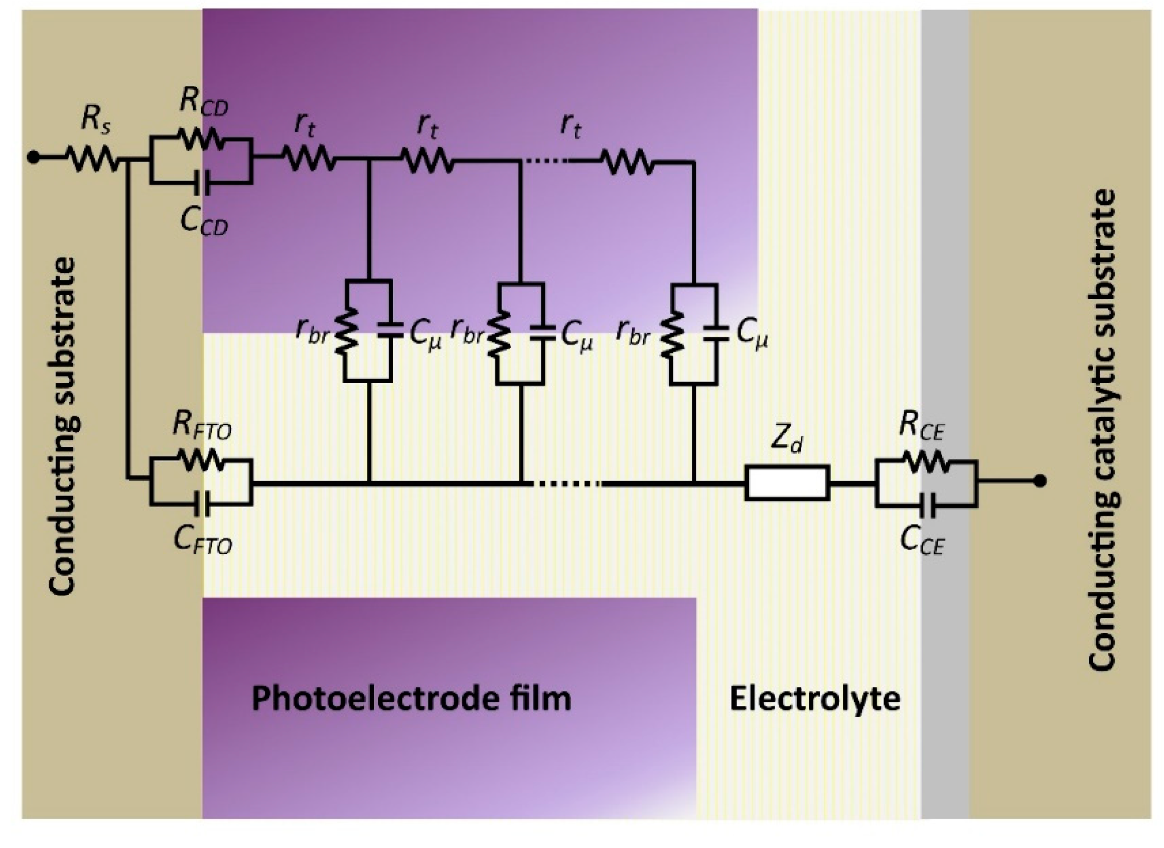
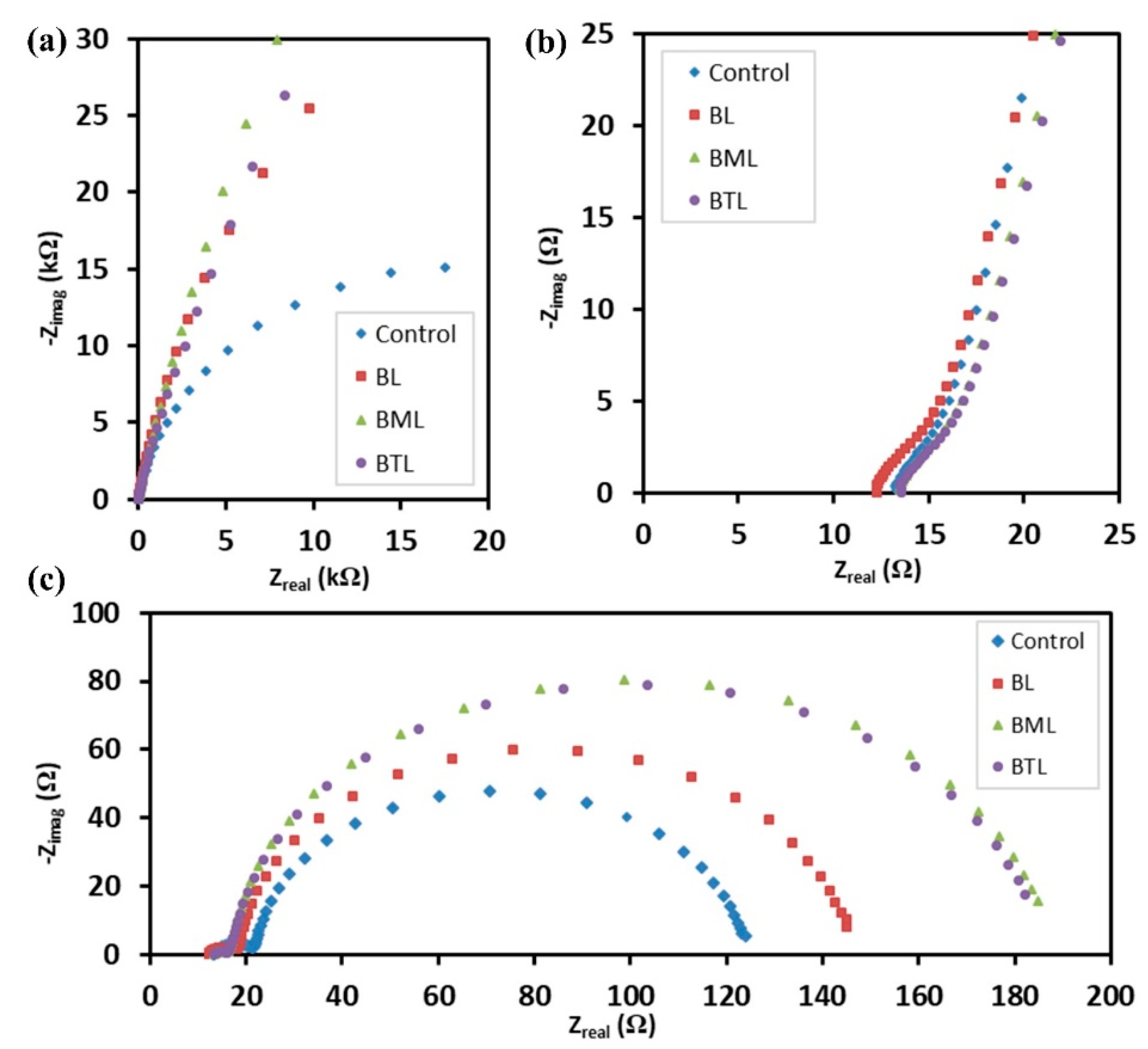
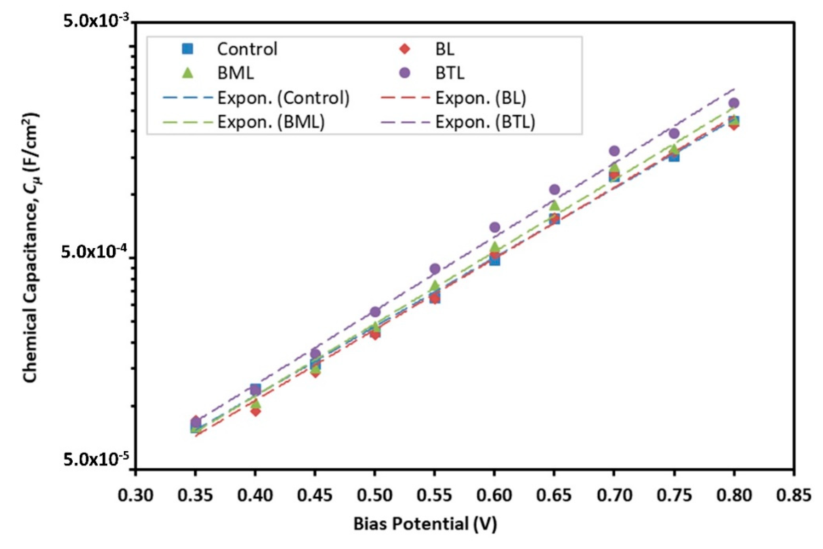
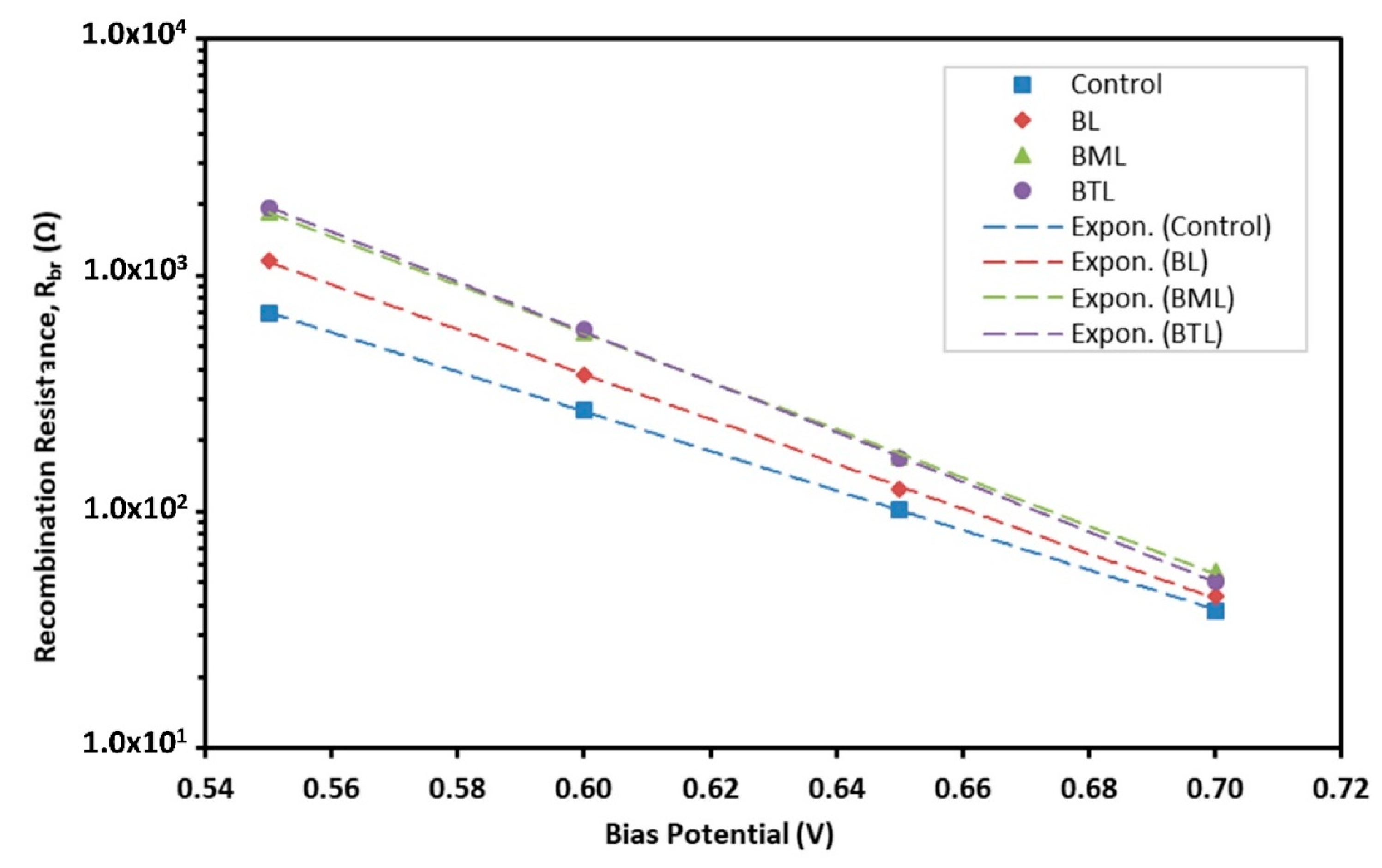
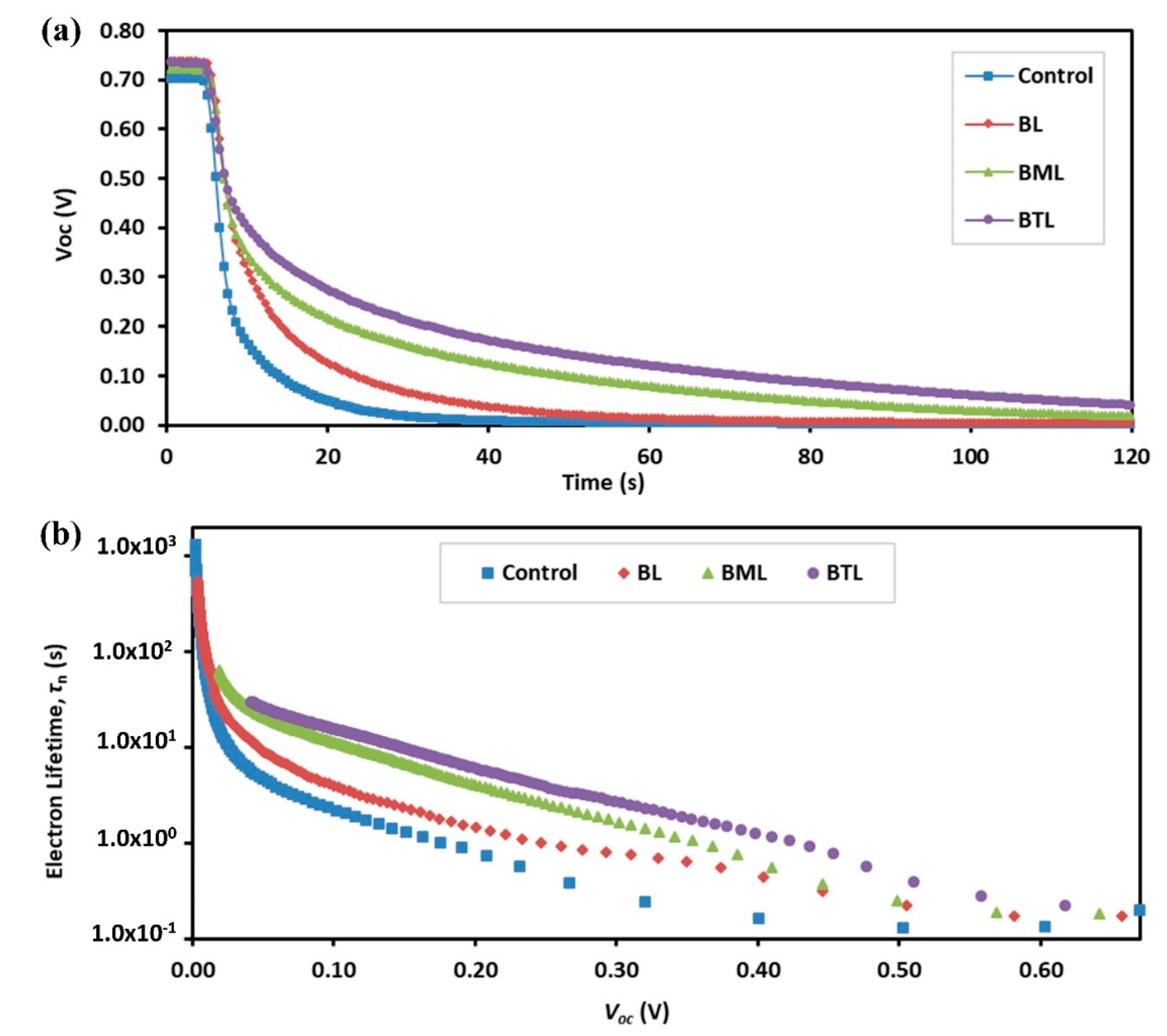
3.2. Electrochemical Analysis

In understanding the electrochemical process of the fabricated DSSC, electrochemical impedance analysis was utilized following the transmission line model [43,44], as illustrated in Figure 7. The model consisted of Rbr (summation of rbr), which signified the charge transfer resistance of the recombination process between electrons in the mesoporous oxide film and tri-iodide; furthermore, Cµ was the chemical capacitance of the mesoporous metal oxide film, Rt (summation of rt) was the transport resistance of the electrons in mesoporous oxide film, Zd was the Warburg element, RCE and CCE were the charge-transfer resistance and double-layer capacitance at the counter electrode, respectively, RFTO and CFTO represented the charge-transfer resistance and the corresponding double-layer capacitance at the exposed FTO–electrolyte interface, respectively, RCD and CCD were the resistance and the capacitance at the FTO–TiO2 interface, and Rs was the sheet resistance, including the resistance of the FTO glass and the contact resistance of the cell. Upon forward bias, the electrons were injected from the FTO substrate into the mesoporous network of TiO2 photoelectrode film and charged by electron propagation through the photoelectrode film. A fraction of electrons injected into the conduction band of TiO2 were lost through the reduction process of I3 species in the electrolyte [43].
The fabricated samples were tested at two different bias potentials of 0.30 V and 0.65 V, as shown in Figure 8. At low bias potential (0.30V), the resistance of TiO2 tended to be infinite and, thus, negligible. The contribution to the impedance spectrum was expected to come from the exposed FTO–electrolyte interface (Figure 8a). The small deformation at the high-frequency region (Figure 8b) was contributed by the resistance and double-layer capacitance of the counter electrode. Based on the analysis, the impedance spectra of all nanocrystalline-coated samples were improved, suggesting that the nanocrystalline-coated layer successfully passivized the FTO conductive substrate, thereby reducing the exposed FTO and limiting the recombination process of electrons at the FTO substrate with the oxidized species of electrolyte.
At intermediate bias potential (0.65V), the impedance spectra exhibited two arcs (Figure 8c). The small arc in the high-frequency range signified the impedance properties of electron transport at the platinum counter electrode, whilst the large arc of the Nyquist plot represented the electron transport properties in the mesoporous oxide film and the recombination of the injected electrons from the TiO2 photoelectrode materials to the redox electrolyte. Table 1 summarizes the goodness of fit and the electrochemical properties of the fitted EIS analysis [44,45,46,47,48], consisting of electron transport resistance (Rt), electron transfer resistance related to recombination (Rbr) estimated from the diameter of the central arc, chemical capacitance (Cµ), electron lifetime (τn), rate constant for recombination (k), electron diffusion coefficient (Dn), and steady-state electron density in the conduction band (ns). Here, k is the inverse of the electron lifetime, which was estimated from the product of Rbr and Cµ, whilst Dn, Con, and ns were calculated based on Equations (1), (2), and (3), respectively. Lastly, L, kB, T, q, and A represent the thickness of the printed TiO2 photoelectrode film, Boltzmann constant (1.38 × 10⁻²³ J∙K−1), absolute temperature (298.15 K), elementary charge (1.60 × 10⁻¹⁹ C), and active area of the photoelectrode film, respectively.
D n   = ( R t C μ ) 1
R b r   = k B T q 2 A n s 1 L k = C o n 1 L k .
C o n = k B T q 2 A n s .
The electrochemical analysis showed that ns of the nanocrystalline-coated photoelectrode films showed higher values compared to the uncoated film. The ns was controlled by two main factors, namely, the number of photogenerated electrons and the recombination process of the injected electrons in the conduction band of TiO2 with the oxidized species. As evident in the UV–Vis analysis, the coated photoelectrode film exhibited a higher dye absorption capability, believed to be due to the formation of nanocrystalline TiO2 through the coating process which filled the gaps between the active photoelectrode material, thus increasing the surface area for anchoring a large number of dye molecules. A large number of anchored dye molecules improves the capability of the photoelectrode to capture light radiance and excite more electrons, which are then injected into the conduction band of the mesoporous photoelectrode film.
The increasing trend of electron density with respect to the nanocrystalline-coated samples is correlated to the chemical capacitance based on the Equation (4) [43,45,46,49].
C µ = q e 2 E F E 2 E 1 ( E E F n ) g ( E ) d E q e 2 g ( E F ) ,
where F ( E E F n ) is the occupation factor of the Fermi–Dirac distribution function, while g(E) is the density of state which can be expressed as shown in Equation (5).
g ( E ) = N L k B T o exp [ ( E E c ) / k B T o ] ,  
where NL is the density of localized states, and To is a parameter with a temperature unit that determines the depth of the distribution below the lower edge of the conduction band, Ec. Based on these two equations (Equations (4) and (5)), an exponential distribution of chemical capacitance was derived as expressed in Equation (6) [43,45,46,49].
C µ = C o e x p ( α q e k B T V ) = C o e x p ( q e k B T o V ) ,
where α is the measure of the depth of the trap energy distribution, which is equal to T/To.
Figure 9 shows the measured chemical capacitance of the fabricated cells integrated with the uncoated and nanocrystalline-coated photoelectrode film. The graph clearly shows that all samples exhibited an exponential trend of Cµ as a function of the applied voltage. Based on the analysis, the value of α was estimated to be about 0.236 for the control sample, while BL, BML, and BTL samples exhibited α values of about 0.224, 0.218, and 0.220, respectively. The analysis indicated that the coating process, whether on the FTO substrate only or on both the FTO substrate and the photoelectrode material, resulted in a slight reduction in the α value. A smaller value of α indicates a wider distribution of the trap states, which signifies the suppression of the trapping/de-trapping process of injected electrons in the conduction band of TiO2 [43,48,50].
Referring to Table 1, the BL sample showed a higher value of Rbr compared to the uncoated samples. This was due to the presence of nanolayer of nanocrystalline TiO2 (Figure 3b), which prevented the recombination of electrons with the oxidized species of electrolyte through the exposed FTO–electrolyte interface. Furthermore, the nanocrystalline TiO2 layer helped to further increase the value of Rbr. The results in Table 1 show that the Rbr values of BML and BTL samples were approximately one-third higher compared to the uncoated DSSC sample. Both samples also exhibited about two-fold lower rates of electron recombination compared to the uncoated photoelectrode-based DSSC and, hence, a doubled lifetime of electrons. The improvements in Rbr and k were related to the improvement of photoelectrode cracking, leading to an enhancement of the connectivity of the photoelectrode network, as evidenced by the FE-SEM analysis in Figure 4, thus improving the electron transfer process and preventing the injected electrons from recombining with the oxidized species. Moreover, the deviation in the Rbr might have resulted in the variation of the saturation current, which is directly proportional to the recombination rate and inversely proportional to the Voc [6]. High recombination resistance helps in reducing the rate of the recombination process and improving electron lifetime. However, the presence of nanocrystalline coating led to a higher Rt, thereby reducing the electron diffusion coefficient. This was due to the presence of more grain boundaries, thus increasing the transport resistance.
The charge transfer resistance related to recombination is exponentially dependent on the bias potential [51,52,53], which can be described by Equation (7).
R br   = R o exp ( β qV corr k B T ) ,
where Ro is a constant, while β is transfer coefficient which explains the sublinear recombination kinetics [51,52] of the DSSC. In order to gain an in-depth understanding of the recombination kinetics, EIS analysis was carried out in the bias potential range of 0.70 V to 0.55 V. Figure 10 shows the recombination resistance of the nanocrystalline-coated and un-coated samples as a function of bias voltage obtained from the EIS analysis tested in dark conditions.
Based on the analysis, all of the integrated DSSCs, whether coated or uncoated sample, showed a typical property of nonlinear recombination with β <1 [43]. The β of the uncoated sample was calculated to be about 0.499, while the nanocrystalline-coated samples exhibited values of 0.565, 0.607, and 0.630 for BL, BML, and BTL, respectively. β is inversely proportional to the diode ideality factor, n, and directly proportional to the fill factor, FF [51]. Thus, the improved β value of the nanocrystalline-coated photoelectrode samples reflected an enhancement of the electrical and electrochemical properties associated with the electron transfer process and internal resistance of the integrated cell. The analysis showed that the nanocrystalline coating process successfully prevented the recombination process of electrons in the conductive substrate and the recombination of electrons in the conduction band of the photoelectrode material with the oxidized electrolyte species.
An open-circuit voltage decay (OCVD) study was adopted in order to further understand the effect of the nanocrystalline TiO2 layer on the electron lifetime in relation to the recombination phenomenon of the fabricated DSSC. The OCVD analysis was done by measuring the voltage decay with respect to time through the exposure of the test cells to the simulated solar radiation at one sun. This analysis can provide detailed information on the electron recombination time in relation to electron trapping and de-trapping, as well as other possible interfacial charge transfer [21,49,54,55,56,57].
Figure 11a shows the OCVD curve of the fabricated DSSC with and without the nanocrystalline TiO2 layer. The plot for the test cell with the nanocrystalline TiO2 layer exhibited a higher open-circuit voltage and a slower decay compared to that without, signifying a slower recombination process of conduction-band electrons with the oxidized species in the electrolyte. From the analysis, electron lifetime with respect to open-circuit voltage, τn, was derived based on the decay curve normalized by the thermal voltage according to Equation (8).
τ n = k B T q ( dV oc dt ) 1 .
Figure 11b shows the logarithmic plot of the electron lifetime with respect to open-circuit voltage decay. The plot could be divided into three different voltage regions. The high-voltage region usually occurred with nearly constant electron lifetime, which represented the recombination process dominated by free electrons in the conduction band states. The exponential growth in the middle of the curve indicated the trapping/de-trapping phenomenon governed by the conduction band transfer. In the low-voltage region, the electron lifetime exhibited a parabolic trend. This region signified the recombination of electrons at the Fermi level through the surface state [49,54,58].
The analysis showed that all samples exhibited an insignificant difference in the lifetime of electrons in the high-voltage region. This condition suggests that all samples experienced almost the same trend of recombination of free electrons at the conduction band state, regardless of whether the photoelectrode was with or without the nanocrystalline TiO2 layer. In comparison, the test cell with a nanocrystalline TiO2 layer on the surface of FTO (BL) exhibited a better electron lifetime than the control sample in the parabolic region. This is because the thin layer of nanocrystalline TiO2 deposited on the FTO substrate suppressed the electron recombination at the exposed FTO–electrolyte interface, as observed in the Nyquist plot of Figure 8a. This finding indicates that the trend of the parabolic region not only contributed to the surface state recombination but also to the dark current phenomenon [59,60]. A further improvement in the electron lifetime of BML and BTL samples was due to the presence of the nanocrystalline coating, which acted as a bridge, connecting the TiO2 nanoparticles, thus improving the transportation of charges. The improvement in charge transport led to a reduced rate of electron recombination, increased the recombination resistance, and improved the lifetime of the electrons. Moreover, the improvement in electron lifetime in the middle region of BML and BTL plots suggests that the nanocrystalline TiO2 layer successfully reduced the trapping/de-trapping phenomenon of generated electrons that took place through bulk traps due to the presence of a shallow distribution of trap state.

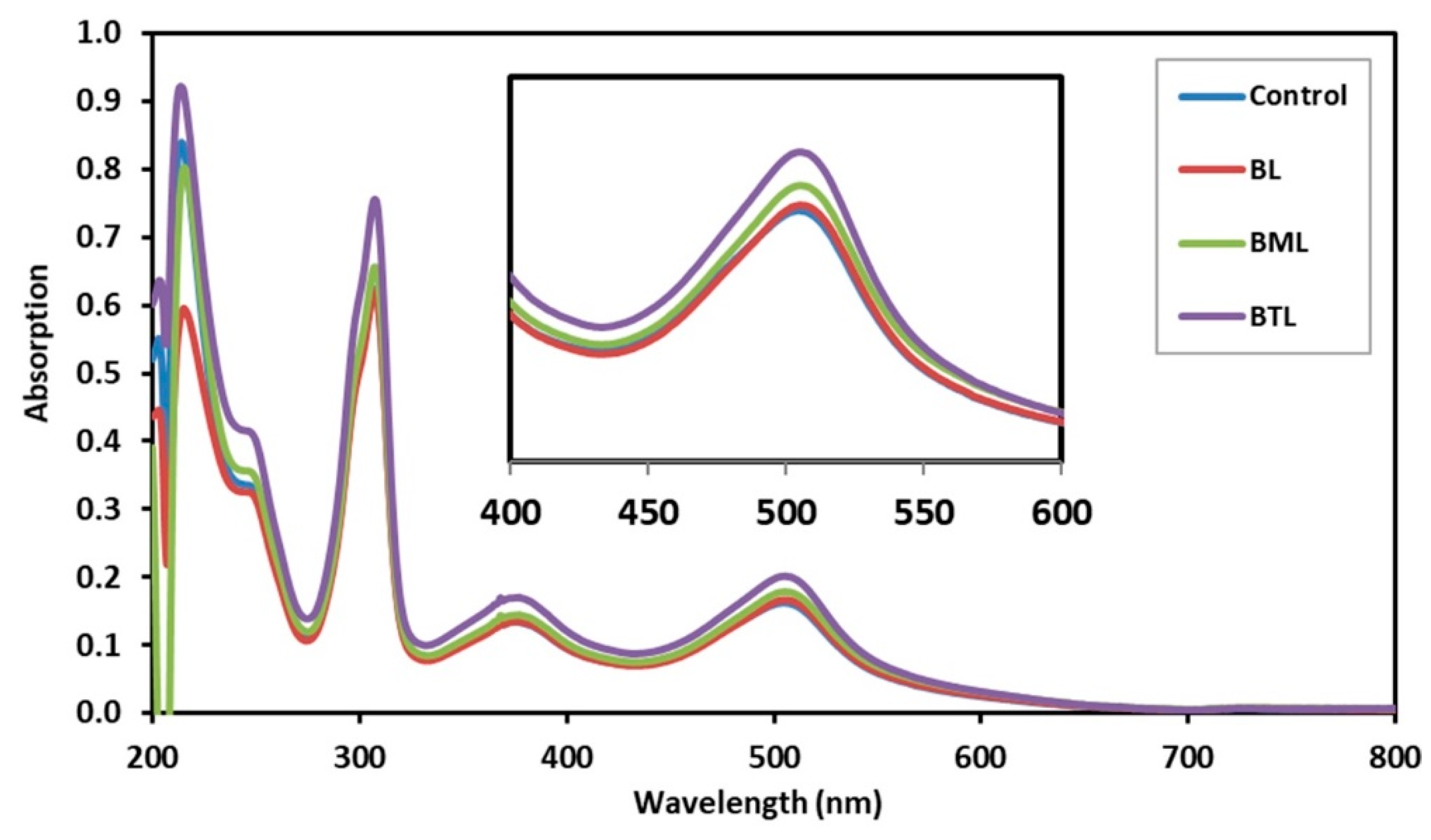
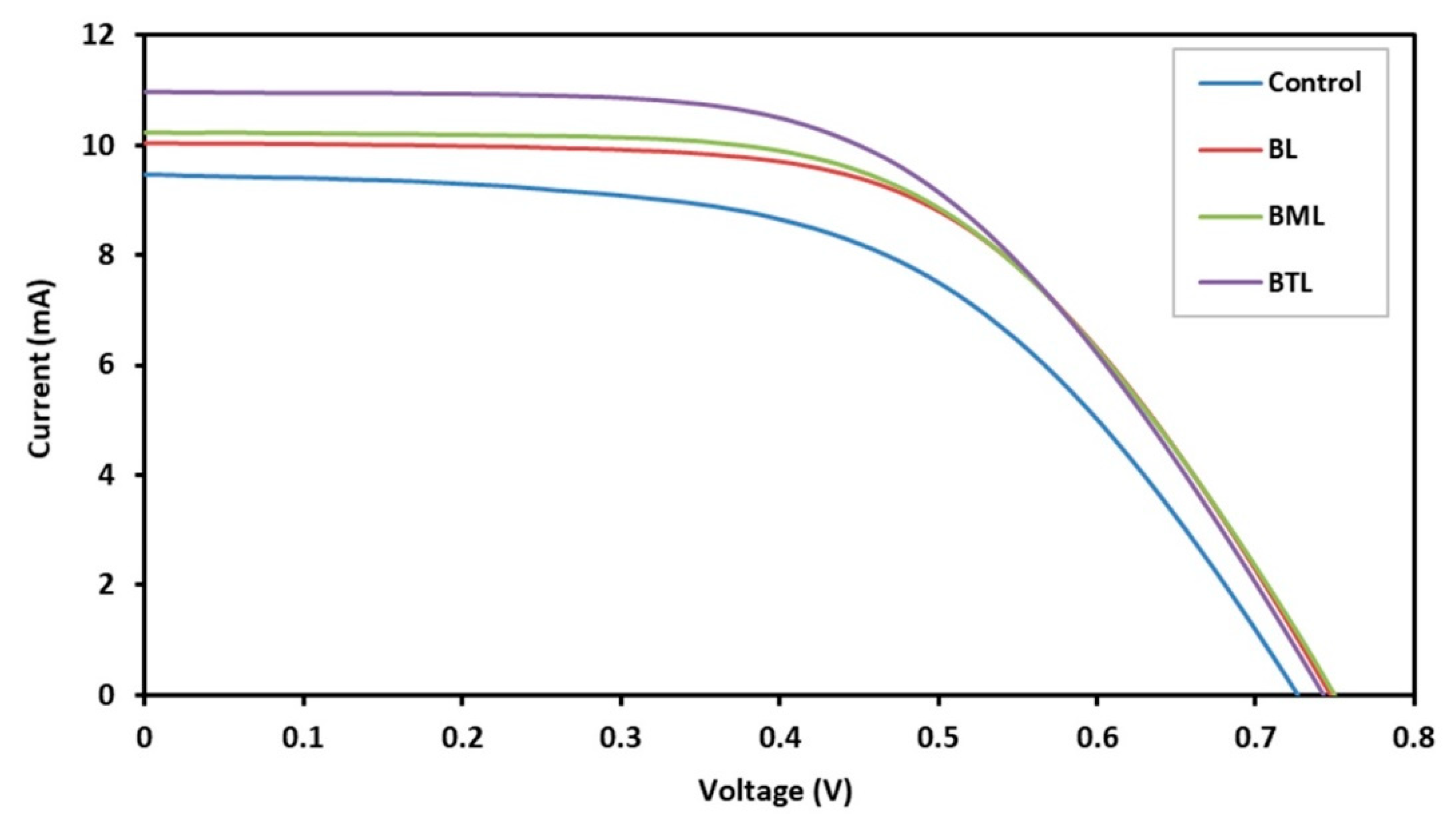
3.3. Photovoltaic Performance

The performance of the integrated cells was evaluated using a universal photovoltaic test system (UPTS) under 1000 W/m2 intensity of simulated solar illumination. Figure 12 shows the I–V plot of the tested cells, whilst the corresponding photovoltaic parameters such as short-circuit current (Isc), open-circuit voltage (Voc), fill factor (FF), and performance efficiency (η) are tabulated in Table 2. The I–V analysis shows that samples with the nanocrystalline TiO2-coated layer successfully improved the Isc, Voc, and FF. The highest FF was achieved by the sample with a nanocrystalline TiO2 layer on the FTO substrate only (BL), whilst the highest Voc was recorded by the sample deposited with the nanocrystalline TiO2-coated layer on the FTO substrate and after deposition of the first layer of the photoelectrode film (BML). In contrast, the highest Isc was recorded by the sample with a nanocrystalline TiO2-coated layer on the FTO substrate and on the second layer of the photoelectrode film, which exhibited the highest performance efficiency of 4.581%, representing an approximately 22% improvement in overall performance efficiency. The enhancement of short-circuit current of the nanocrystalline-coated photoelectrode sample was attributed to the increase in the amount of absorbed dye, which led to an increase in the number of generated electrons, which increased the electron density in the conduction band of TiO2. Furthermore, the improvement in electron transport properties and internal resistance of the fabricated DSSC consisting of the nanocrystalline TiO2 passivation layer improved its photovoltaic properties related to FF and Voc.

4. Conclusions

The dipped coating process successfully formed a thin nanocrystalline TiO2 layer on the surface of the FTO substrate and TiO2 photoelectrode film. The nanocrystalline coating process helped to improve film packing and reduce film cracking, thus increasing the surface area for the dye absorption process. Furthermore, the coating also acted as a passivation layer, suppressing back electron transfer and improving the overall performance of the integrated DSSC. The suppression of back electron transport was related to the reduction of the exposed FTO–electrolyte interface, which reduced the dark current phenomenon. In addition, the presence of the passivation layer on the surface of the photoelectrode film helped to increase the recombination resistance and reduces the rate of recombination of electrons related to the surface state recombination, as well as the trapping/de-trapping phenomenon. Increasing the dye absorption capability and improving the internal resistance of integrated cells helped to increase the steady-state electron density, reduce the effective rate of recombination, and improve the lifetime of electrons, thereby improving the photovoltaic properties and performance efficiency of the DSSC. Based on this study, the optimum configuration of the photoelectrode DSSC involves the nanocrystalline TiO2 passivation layer at the top of the FTO substrate and after the deposition of the second photoelectrode layer (BTL). This optimum configuration exhibited the highest performance efficiency of 4.581%, representing an approximately 22% improvement in the overall performance efficiency compared to the control sample.

Author Contributions

Conceptualization, S.N.A.Z. and N.M.M.; methodology, S.N.A.Z.; formal analysis, S.N.A.Z., M.K., A.E.S., and M.U.S.; data curation, S.N.A.Z., M.K., A.E.S., and M.U.S.; writing—original draft preparation, S.N.A.Z.; writing—review and editing, N.M.M.; supervision, N.M.M.; All authors read and agreed to the published version of the manuscript.

Funding

The authors would like to acknowledge Universiti Teknologi PETRONAS, the Ministry of Education (MOE) and Ministry of Energy, Science, Technology, Environment, and Climate Change (MESTECC), Malaysia, for funding the research under the Short-Term Internal Research Fund (015LA0-017), MyRa Incentive Grant for Smart iLoci Model Project and TechnoFund Project (TF1113D338).

Acknowledgments

The authors would like to acknowledge the Centralized Analytical Laboratory of Universiti Teknologi PETRONAS for the FE-SEM and XRD analyses.

Conflicts of Interest

The authors declare no conflicts of interest.

References

  1. Grätzel, M. Solar energy conversion by dye-sensitized photovoltaic cells. Inorg. Chem. 2005, 44, 6841–6851. [Google Scholar]
  2. Nazeeruddin, M.K.; Baranoff, E.; Grätzel, M. Dye-sensitized solar cells: A brief overview. Sol. Energy 2011, 85, 1172–1178. [Google Scholar] [CrossRef]
  3. Lau, K.K.; Soroush, M. Overview of dye-sensitized solar cells in Dye-Sensitized Solar Cells; Academic Press: Cambridge, MA, USA, 2019; pp. 1–49. [Google Scholar]
  4. Karim, N.A.; Mehmood, U.; Zahid, H.F.; Asif, T. Nanostructured photoanode and counter electrode materials for efficient Dye-Sensitized Solar Cells (DSSCs). Sol. Energy 2019, 185, 165–188. [Google Scholar] [CrossRef]
  5. Jose, R.; Thavasi, V.; Ramakrishna, S. Metal oxide for dye-sensitized solar cells. J. Am. Ceram. Soc. 2009, 92, 289–301. [Google Scholar] [CrossRef]
  6. Zhang, S.; Yang, X.; Numata, Y.; Han, L. Highly efficient dye-sensitized solar cells: progress and future challenges. Energy Environ. Sci. 2013, 6, 1443–1464. [Google Scholar] [CrossRef]
  7. Gong, J.; Liang, J.; Sumathy, K. Review on dye-sensitized solar cells (DSSCs): Fundamental concepts and novel materials. Renew. and Sustain. Energy Rev. 2012, 16, 5848–5860. [Google Scholar] [CrossRef]
  8. Afrooz, M.; Dehghani, H.; Khalili, S.S.; Firoozi, N. Effects of cobalt ion doped in the ZnS passivation layer on the TiO2 photoanode in dye sensitized solar cells based on different counter electrodes. Synth. Met. 2017, 226, 164–170. [Google Scholar] [CrossRef]
  9. Ako, R.T.; Ekanayake, P.; Tan, A.L.; Young, D.J. La modified TiO2 photoanode and its effect on DSSC performance: A comparative study of doping and surface treatment on deep and surface charge trapping. Mater. Chem. and Phys. 2016, 172, 105–112. [Google Scholar] [CrossRef]
  10. D'Souza, L.P.; Shwetharani, R.; Amoli, V.; Fernando, C.A.N.; Sinha, A.K.; Balakrishna, R.G. Photoexcitation of neodymium doped TiO2 for improved performance in dye-sensitized solar cell. Mater. & Design 2016, 104, 346–354. [Google Scholar]
  11. Xiang, P.; Ma, W.; Xiao, T.; Jiang, L.; Tan, X.; Shu, T. Ta-doped hierarchical TiO2 spheres for dye-sensitized solar cells. J. Alloy Compd. 2016, 656, 45–50. [Google Scholar] [CrossRef]
  12. Zhou, L.; Wei, L.; Yang, Y.; Xia, X.; Wang, P.; Yu, J.; Luan, T. Improved performance of dye sensitized solar cells using Cu-doped TiO2 as photoanode materials: Band edge movement study by spectroelectrochemistry. Chem. Phys. 2016, 475, 1–8. [Google Scholar] [CrossRef]
  13. Park, J.Y.; Kim, C.S.; Okuyama, K.; Lee, H.M.; Jang, H.D.; Lee, S.E.; Kim, T.O. Copper and nitrogen doping on TiO2 photoelectrodes and their functions in dye-sensitized solar cells. J. Power Sources 2016, 306, 764–771. [Google Scholar] [CrossRef]
  14. Khaki, M.R.D.; Shafeeyan, M.S.; Raman, A.A.A.; Daud, W.M.A.W. Evaluating the efficiency of nano-sized Cu doped TiO2/ZnO photocatalyst under visible light irradiation. J. Mol. Liq. 2018, 258, 354–365. [Google Scholar] [CrossRef]
  15. Rajaei, E.; Ravandi, S.A.H.; Valipouri, A. Electrochemical and photovoltaic properties of dye-sensitized solar cells based on Ag-doped TiO2 nanorods. Optik 2018, 158, 514–521. [Google Scholar] [CrossRef]
  16. Ünlü, B.; Çakar, S.; Özacar, M. The effects of metal doped TiO2 and dithizone-metal complexes on DSSCs performance. Sol. Energy 2018, 166, 441–449. [Google Scholar] [CrossRef]
  17. Tyona, M.D.; Jambure, S.B.; Lokhande, C.D.; Banpurkar, A.G.; Osuji, R.U.; Ezema, F.I. Dye-sensitized solar cells based on Al-doped ZnO photoelectrodes sensitized with rhodamine. Mater. Lett. 2018, 220, 281–284. [Google Scholar] [CrossRef]
  18. Kouhestanian, E.; Mozaffari, S.A.; Ranjbar, M.; SalarAmoli, H.; Armanmehr, M.H. Electrodeposited ZnO thin film as an efficient alternative blocking layer for TiCl4 pre-treatment in TiO2-based dye sensitized solar cells. Superlattices Microstruct. 2016, 96, 82–94. [Google Scholar] [CrossRef]
  19. Ranasinghe, C.S.K.; Jayaweera, E.N.; Kumara, G.R.A.; Rajapakse, R.M.G.; Onwona-Agyeman, B.; Perera, A.G.U.; Tennakone, K. Tin oxide based dye-sensitized solid-state solar cells: surface passivation for suppression of recombination. Mater. Sci. Semicond. Process. 2015, 40, 890–895. [Google Scholar] [CrossRef]
  20. Li, J.; Zhang, H.; Wang, W.; Qian, Y.; Li, Z. Improved performance of dye-sensitized solar cell based on TiO2 photoanode with FTO glass and film both treated by TiCl4. Phys. B Condens. Matter 2016, 500, 48–52. [Google Scholar]
  21. Xiang, Y.; Yu, J.; Zhang, T.; Wen, Q.; Zhuang, J.; Guo, J. Improved performance of nanoporous TiO2 film in dye-sensitized solar cells via ZrCl4 and TiCl4 surface co-modifications. Mater. Sci. Semicond. Process. 2016, 49, 48–53. [Google Scholar] [CrossRef]
  22. Choi, H.; Nahm, C.; Kim, J.; Moon, J.; Nam, S.; Jung, D.R.; Park, B. The effect of TiCl4-treated TiO2 compact layer on the performance of dye-sensitized solar cell. Curr. Appl. Phys. 2012, 12, 737–741. [Google Scholar] [CrossRef]
  23. Gopakumar, G.; Ashok, A.; Vijayaraghavan, S.N.; Nair, S.V.; Shanmugam, M. MoO3 surface passivation on TiO2: An efficient approach to minimize loss in fill factor and maximum power of dye sensitized solar cell. Appl. Surf. Sci. 447, 554–560. [CrossRef]
  24. Roose, B.; Pathak, S.; Steiner, U. Doping of TiO2 for sensitized solar cells. Chem. Soc. Rev. 2015, 44, 8326–8349. [Google Scholar] [CrossRef] [PubMed] [Green Version]
  25. Pascoe, A.R.; Bourgeois, L.; Duffy, N.W.; Xiang, W.; Cheng, Y.B. Surface state recombination and passivation in nanocrystalline TiO2 dye-sensitized solar cells. J. Phys. Chem. C. 2013, 117, 25118–25126. [Google Scholar] [CrossRef]
  26. Kim, Y.J.; Kim, K.H.; Kang, P.; Kim, H.J.; Choi, Y.S.; Lee, W.I. Effect of layer-by-layer assembled SnO2 interfacial layers in photovoltaic properties of dye-sensitized solar cells. Langmuir 2012, 28, 10620–10626. [Google Scholar] [CrossRef]
  27. Park, J.; Lee, M. Performance enhancement of dye-sensitized solar cell with a TiCl4-treated TiO2 compact layer. Electron. Mater. Lett. 2015, 11, 271–275. [Google Scholar] [CrossRef]
  28. Lee, S.W.; Ahn, K.S.; Zhu, K.; Neale, N.R.; Frank, A.J. Effects of TiCl4 treatment of nanoporous TiO2 films on morphology, light harvesting, and charge-carrier dynamics in dye-sensitized solar cells. J. Phys. Chem. C 2012, 116, 21285–21290. [Google Scholar] [CrossRef]
  29. Charoensirithavorn, P.; Ogomi, Y.; Sagawa, T.; Hayase, S.; Yoshikawa, S. Improvement of dye-sensitized solar cell through TiCl4-treated TiO2 nanotube arrays. J. Electrochem. Soc. 2010, 157, B354–B356. [Google Scholar] [CrossRef]
  30. Wang, J.; Lin, Z. Dye-sensitized TiO2 nanotube solar cells with markedly enhanced performance via rational surface engineering. Chem. Mater. 2010, 22, 579–584. [Google Scholar]
  31. Fuke, N.; Katoh, R.; Islam, A.; Kasuya, M.; Furube, A.; Fukui, A.; Chiba, Y.; Komiya, R.; Yamanaka, R.; Han, L. Influence of TiCl4 treatment on back contact dye-sensitized solar cells sensitized with black dye. Energy & Environ. Sci. 2009, 2, 1205–1209. [Google Scholar]
  32. Knorr, F.J.; Zhang, D.; McHale, J.L. Influence of TiCl4 treatment on surface defect photoluminescence in pure and mixed-phase nanocrystalline TiO2. Langmuir 2007, 23, 8686–8690. [Google Scholar] [CrossRef] [PubMed]
  33. O'Regan, B.C.; Durrant, J.R.; Sommeling, P.M.; Bakker, N.J. Influence of the TiCl4 treatment on nanocrystalline TiO2 films in dye-sensitized solar cells. 2. Charge density, band edge shifts, and quantification of recombination losses at short circuit. J. Phys. Chem. 2007, 111, 14001–14010. [Google Scholar] [CrossRef]
  34. Sommeling, P.M.; O'Regan, B.C.; Haswell, R.R.; Smit, H.J.P.; Bakker, N.J.; Smits, J.J.T.; Kroon, J.M.; Van Roosmalen, J.A.M. Influence of a TiCl4 post-treatment on nanocrystalline TiO2 films in dye-sensitized solar cells. J. Phys. Chem. B vol. 2006, 110, 19191–19197. [Google Scholar] [CrossRef] [PubMed]
  35. Roy-Mayhew, J.D.; Aksay, I.A. Graphene materials and their use in dye-sensitized solar cells. Chem. Rev. 2014, 114, 6323–6348. [Google Scholar] [CrossRef]
  36. Chen, T.; Hu, W.; Song, J.; Guai, G.H.; Li, C.M. Interface functionalization of photoelectrodes with graphene for high performance dye-sensitized solar cells. Adv. Funct. Mater. 2012, 22, 5245–5250. [Google Scholar] [CrossRef]
  37. Tang, B.; Hu, G. Two kinds of graphene-based composites for photoanode applying in dye-sensitized solar cell. J. Power Sources 2012, 220, 95–102. [Google Scholar] [CrossRef]
  38. Durantini, J.; Boix, P.P.; Gervaldo, M.; Morales, G.M.; Otero, L.; Bisquert, J.; Barea, E.M. Photocurrent enhancement in dye-sensitized photovoltaic devices with titania–graphene composite electrodes. J. Electroanal. Chem. 2012, 683, 43–46. [Google Scholar] [CrossRef]
  39. Zhang, D.W.; Li, X.D.; Li, H.B.; Chen, S.; Sun, Z.; Yin, X.J.; Huang, S.M. Graphene-based counter electrode for dye-sensitized solar cells Carbon 2011, 49, 5382–5388. Carbon 2011, 49, 5382–5388. [Google Scholar] [CrossRef]
  40. Kim, S.R.; Parvez, M.K.; Chhowalla, M. UV-reduction of graphene oxide and its application as an interfacial layer to reduce the back-transport reactions in dye-sensitized solar cells. Chem. Phys. Lett. 2009, 483, 124–127. [Google Scholar] [CrossRef]
  41. Ito, S.; Chen, P.; Comte, P.; Nazeeruddin, M.K.; Liska, P.; Péchy, P.; Grätzel, M. Fabrication of screen-printing pastes from TiO2 powders for dye-sensitised solar cells. Prog. in Photovolt. Res. Appl. 2007, 15, 603–612. [Google Scholar] [CrossRef]
  42. Agarwala, S.; Kevin, M.; Wong, A.S.W.; Peh, C.K.N.; Thavasi, V.; Ho, G.W. Mesophase ordering of TiO2 film with high surface area and strong light harvesting for dye-sensitized solar cell. ACS Appl. Mater. & Interfaces 2010, 2, 1844–1850. [Google Scholar]
  43. Wang, Q.; Ito, S.; Grätzel, M.; Fabregat-Santiago, F.; Mora-Sero, I.; Bisquert, J.; Bessho, T.; Imai, H. Characteristics of high efficiency dye-sensitized solar cells. J. Phys. Chem. B 2006, 110, 25210–25221. [Google Scholar] [CrossRef]
  44. Adachi, M.; Sakamoto, M.; Jiu, J.; Ogata, Y.; Isoda, S. Determination of parameters of electron transport in dye-sensitized solar cells using electrochemical impedance spectroscopy. J. Phys. Chem. B 2006, 110, 13872–13880. [Google Scholar] [CrossRef]
  45. MORA-SERO, I.V.A.N. Characterization of capacitance, transport and recombination parameters in hybrid perovskite and organic solar cells in Unconventional Thin Film Photovoltaics; The Royal Society of Chemistry: London, UK, 2016; Chapter 3; pp. 57–106. [Google Scholar]
  46. Bisquert, J. Theory of the impedance of charge transfer via surface states in dye-sensitized solar cells. J. Electroanal. Chem. 2010, 646, 43–51. [Google Scholar] [CrossRef]
  47. Bisquert, J. Theory of the impedance of electron diffusion and recombination in a thin layer. J. Phys. Chem. B 2002, 106, 325–333. [Google Scholar] [CrossRef]
  48. Bisquert, J. Chemical capacitance of nanostructured semiconductors: Its origin and significance for nanocomposite solar cells. Phys. Chem. Chem. Phys. 2003, 5, 5360–5364. [Google Scholar] [CrossRef]
  49. Bisquert, J.; Zaban, A.; Greenshtein, M.; Mora-Seró, I. Determination of rate constants for charge transfer and the distribution of semiconductor and electrolyte electronic energy levels in dye-sensitized solar cells by open-circuit photovoltage decay method. J. Am. Ceram. Soc 2004, 126, 13550–13559. [Google Scholar] [CrossRef]
  50. Fabregat-Santiago, F.; Randriamahazaka, H.; Zaban, A.; Garcia-Canadas, J.; Garcia-Belmonte, G.; Bisquert, J. Chemical capacitance of nanoporous-nanocrystalline TiO2 in a room temperature ionic liquid. Phys. Chem. Chem. Phys. 2006, 8, 1827–1833. [Google Scholar] [CrossRef]
  51. Bisquert, J.; Mora-Seró, I. Simulation of steady-state characteristics of dye-sensitized solar cells and the interpretation of the diffusion length. J. Phys. Chem. Lett. 2010, 1, 450–456. [Google Scholar] [CrossRef]
  52. Agosta, R.; Giannuzzi, R.; De Marco, L.; Manca, M.; Belviso, M.R.; Cozzoli, P.D.; Gigli, G. Electrochemical assessment of the band-edge positioning in shape-tailored TiO2-nanorod-based photoelectrodes for dye solar cells. J. Phys. Chem. C 2013, 117, 2574–2583. [Google Scholar] [CrossRef] [Green Version]
  53. Agosta, R.; Giannuzzi, R.; De Marco, L.; Manca, M.; Belviso, M.R.; Cozzoli, P.D.; Gigli, G. Valence band edge shifts and charge-transfer dynamics in Li-doped NiO based p-type DSSCs. Electrochim. Acta 2016, 188, 309–316. [Google Scholar]
  54. Zaban, A.; Greenshtein, M.; Bisquert, J. Determination of the electron lifetime in nanocrystalline dye solar cells by open-circuit voltage decay measurement. Chem. Phys. Chem. 2003, 4, 859–864. [Google Scholar] [CrossRef] [PubMed]
  55. Bisquert, J.; Fabregat-Santiago, F.; Mora-Sero, I.; Garcia-Belmonte, G.; Gimenez, S. Electron lifetime in dye-sensitized solar cells: Theory and interpretation of measurements. J. Phys. Chem. C 2009, 113, 17278–17290. [Google Scholar] [CrossRef]
  56. Manjceevan, A.; Bandara, J. Robust surface passivation of trap sites in PbS q-dots by controlling the thickness of CdS layers in PbS/CdS quantum dot solar cells. Sol. Energy Mater. Sol. Cells 2016, 147, 157–163. [Google Scholar] [CrossRef]
  57. Sun, X.; Zhou, X.; Xu, Y.; Sun, P.; Huang, N.; Sun, Y. Mixed P25 nanoparticles and large rutile particles as a top scattering layer to enhance performance of nanocrystalline TiO2 based dye-sensitized solar cell. Appl. Surf. Sci. 2015, 337, 188–194. [Google Scholar] [CrossRef]
  58. Ivanovska, T.; Saponjic, Z.; Radoicic, M.; Ortolani, L.; Morandi, V.; Ruani, G. Improvement of dye solar cell efficiency by photoanode post-treatment. Int. J. Photoenergy 2014, 835760. [Google Scholar]
  59. Ondersma, J.W.; Hamann, T.W. Impedance investigation of dye-sensitized solar cells employing outer-sphere redox shuttles. J. Phys. Chem. C 2010, 114, 638–645. [Google Scholar] [CrossRef]
  60. Ondersma, J.W.; Hamann, T.W. Recombination and redox couples in dye-sensitized solar cells. Coord. Chem. Rev. 2013, 257, 1533–1543. [Google Scholar] [CrossRef]
Figure 1. Illustration of the configuration of the prepared photoelectrode samples.
Coatings 10 00284 g001
Figure 2. (a) The schematic diagram and (b) optical images of an assembled dye-sensitized solar cell (DSSC).
Coatings 10 00284 g002
Figure 3. Field-emission (FE) SEM images of top view of fluorine-doped tin oxide (FTO) substrate (a) before and (b) after being coated with nanocrystalline TiO2; (c) energy-dispersive X-ray spectroscopy (EDX) analysis and (d) element mapping of FTO substrate coated with nanocrystalline TiO2 taken at 100,000× magnification.
Coatings 10 00284 g003
Figure 4. The FE-SEM images of the surface of the TiO2 film (a) before and (b) after being coated with nanocrystalline TiO2, taken at 2000× magnification; (c) the cross-section image of the printed photoelectrode film.
Coatings 10 00284 g004
Figure 5. X-ray diffraction (XRD) spectrum of (a) FTO substrate, (b) FTO substrate treated with TiCl4, (c) TiO2 film on FTO substrate, and (d) TiO2 film on FTO substrate after treatment with TiCl4.
Coatings 10 00284 g005
Figure 6. UV–Vis analysis of the desorbed dye solution of untreated (control) and TiCl4-treated (bottom layer-BL, bottom & middle layer-BML, and bottom & top layer-BTL) samples.
Coatings 10 00284 g006
Figure 7. Equivalent circuit of a dye-sensitized solar cell.
Coatings 10 00284 g007
Figure 8. Nyquist plot of fabricated DSSC integrated with and without nanocrystalline TiO2 layer at (a) and (b) 0.30 V and (c) 0.65 V in the frequency range of 300 kH to 0.1 Hz.
Coatings 10 00284 g008
Figure 9. Chemical capacitance of fabricated samples with and without nanocrystalline TiO2 layer.
Coatings 10 00284 g009
Figure 10. Electron recombination resistance, Rbr, of the fabricated DSSC integrated with and without the nanocrystalline TiO2 layer.
Coatings 10 00284 g010
Figure 11. (a) Open-circuit voltage decay and (b) electron lifetime as a function of Voc.
Coatings 10 00284 g011
Figure 12. I–V curve of the fabricated DSSC integrated with and without nanocrystalline TiO2 layer.
Coatings 10 00284 g012
Table 1. Electrochemical properties of DSSC fabricated without (control sample) and with nanocrystalline TiO2 layer.
SampleGoodness of FitRt (Ω)Rbr (Ω)Cµ(F∙cm−2)τn (s)k (s−1)Dn (cm2∙s−1)Con (Ω∙cm∙s−1)ns (cm−3)
Control1.35 × 10−43.455102.17.61 × 10−40.07812.883.81 × 10−61.5121.07 × 1017
BL1.28 × 10−44.833123.78.21 × 10−40.1029.842.52 × 10−61.4001.15 × 1017
BML1.50 × 10−44.749170.48.89 × 10−40.1526.602.37 × 10−61.2931.25 × 1017
BTL1.40 × 10−45.033168.41.06 × 10−30.1785.631.88 × 10−61.0901.48 × 1017
Table 2. Photovoltaic parameters of the DSSC integrated without (control sample) and with nanocrystalline TiO2 layer. FF—fill factor.
SampleIsc (mA)Voc (V)FF𝜂 (%)
Control9.4580.7280.5463.756
BL10.0420.7480.5874.408
BML10.2170.7510.5774.425
BTL10.9650.7430.5624.581

