Ultrathin Nano-Absorbers in Photovoltaics: Prospects and Innovative Applications


Abstract
1. Introduction
2. Methods and Materials
2.1. Experimental
2.2. Characterization
2.3. Simulation
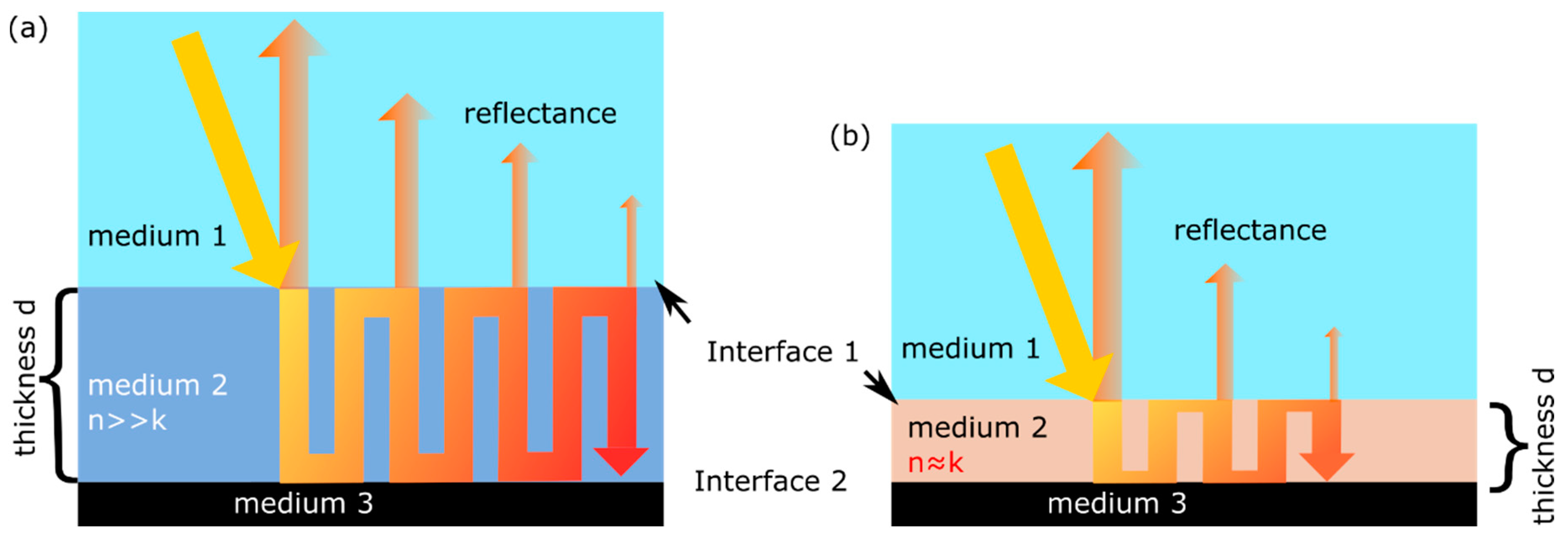
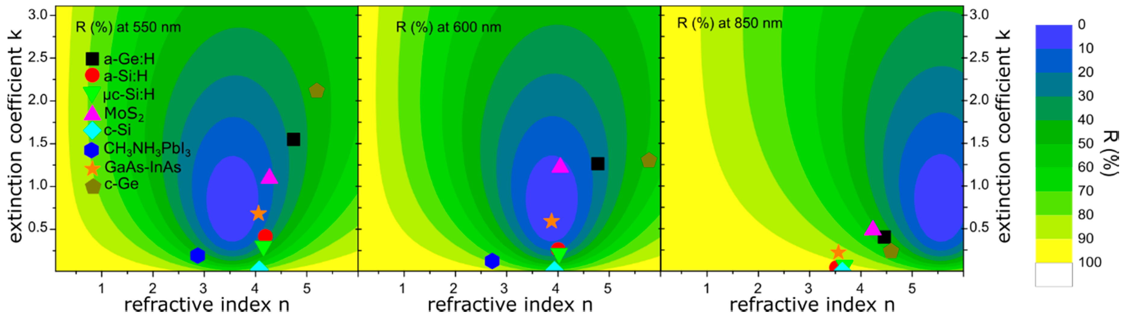
3. Nano Cavity PV
3.1. Fundamentals of Cavity Enhanced Light Absorption
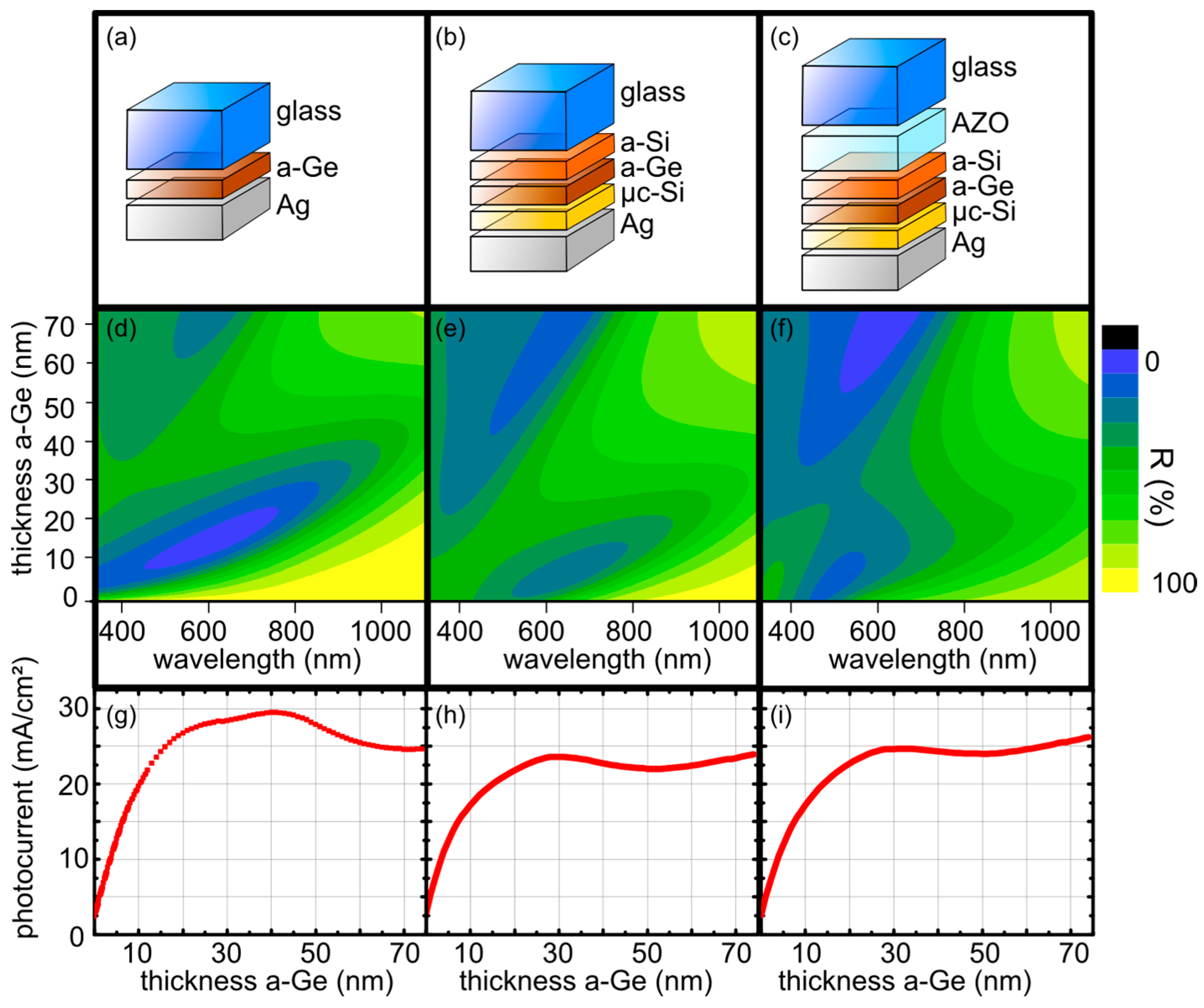
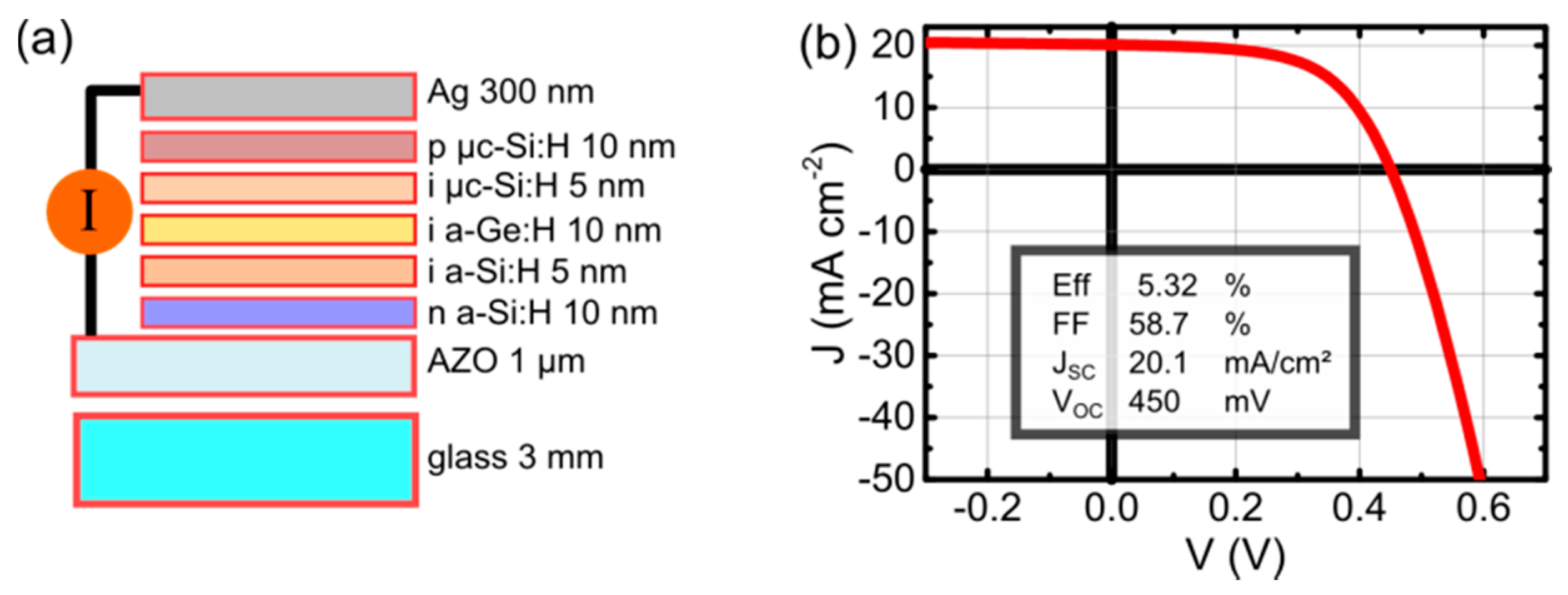
3.2. Amorphous Germanium Solar Cell
3.3. Applications for Photovoltaics with Ultrathin Absorbers
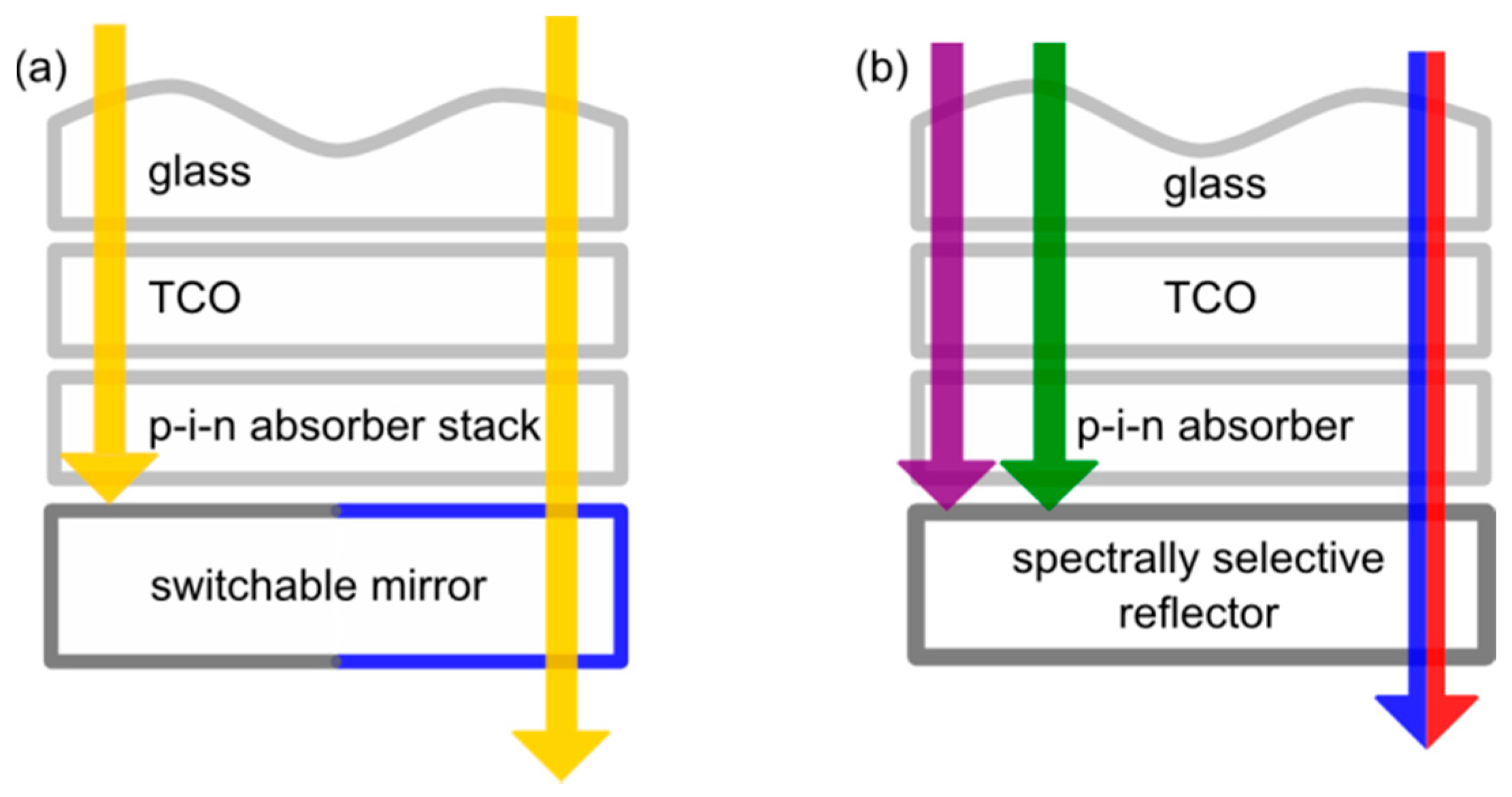
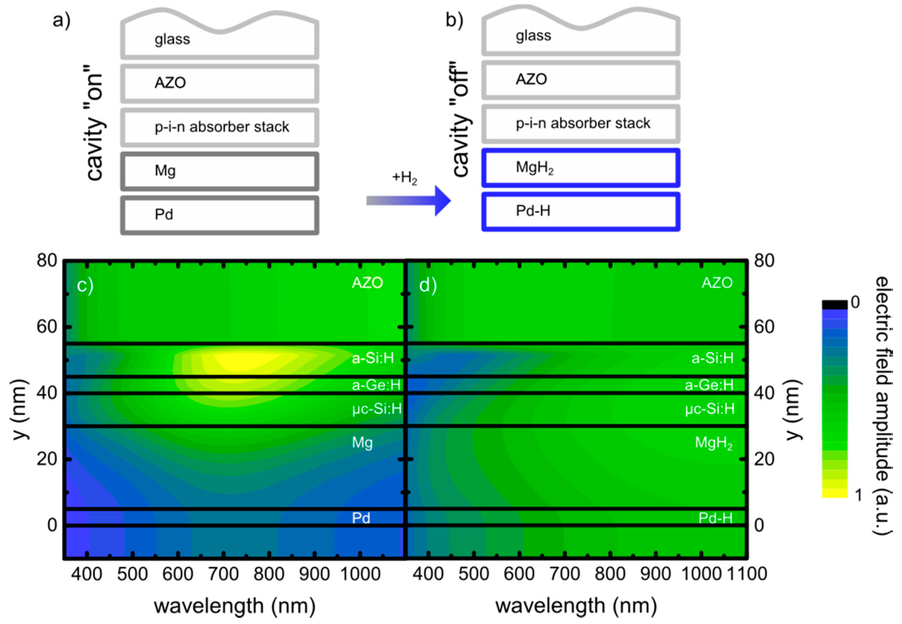
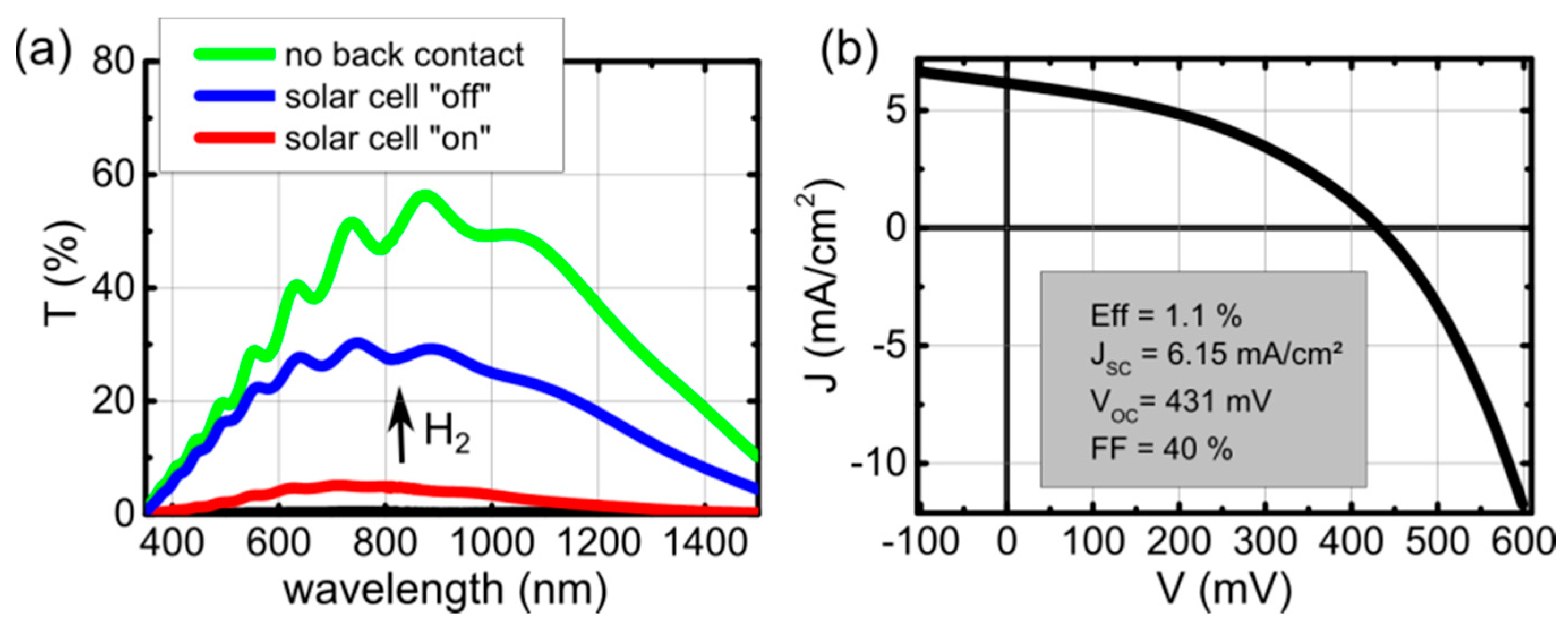
4. Switchable Photovoltaic Windows
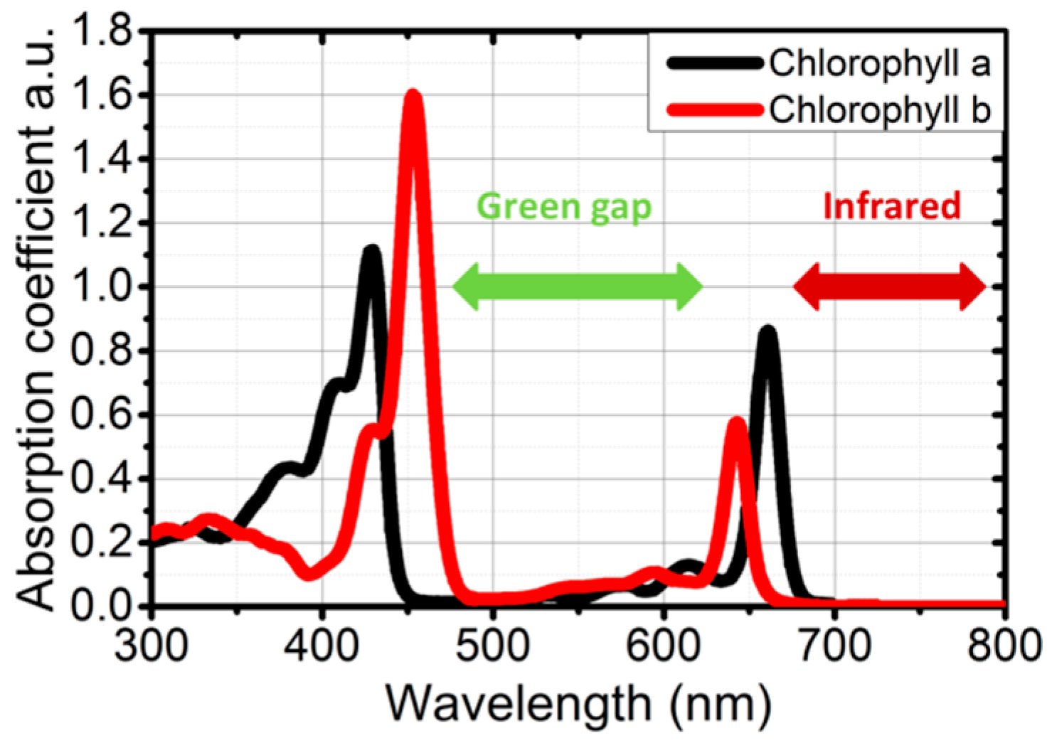
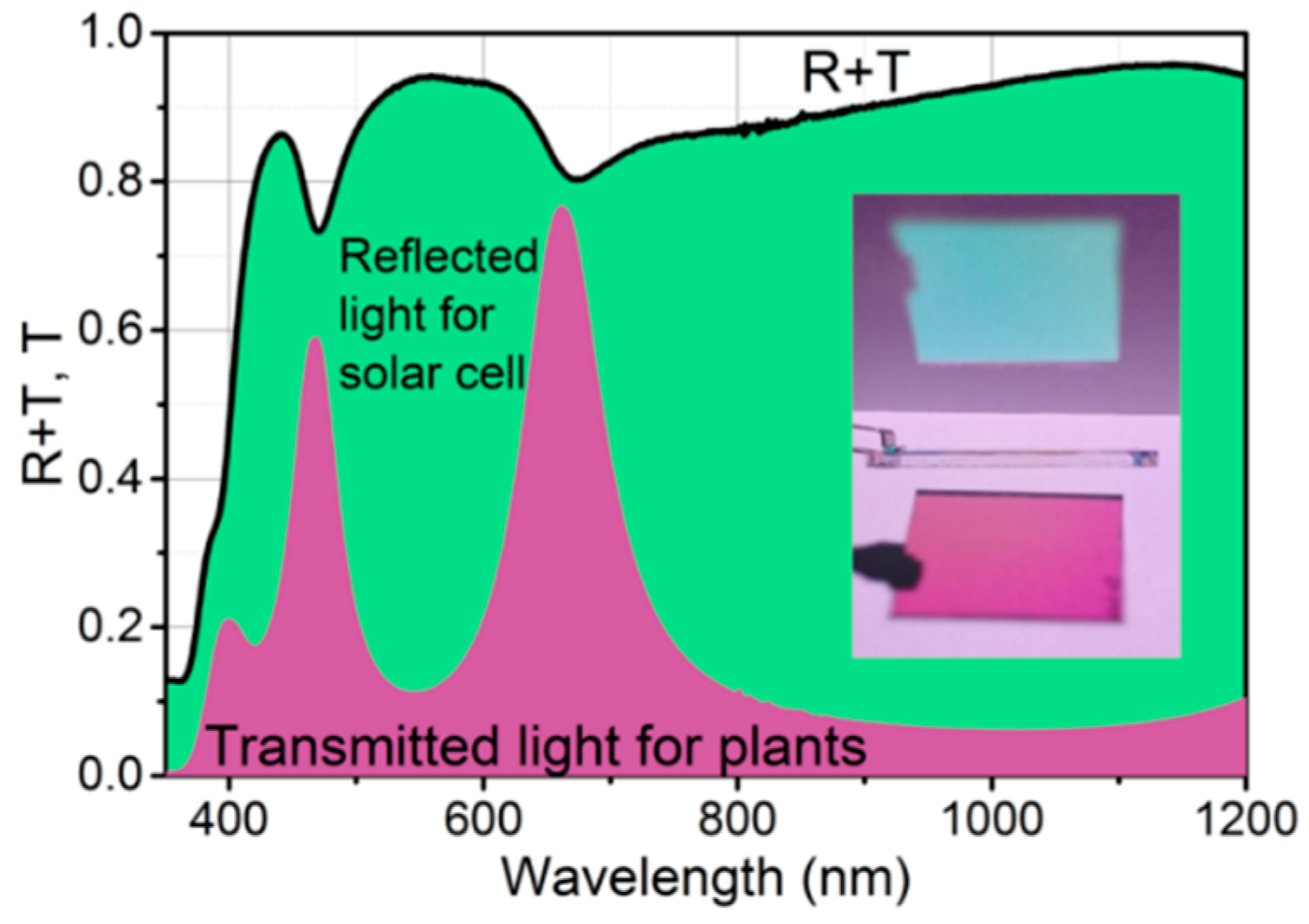
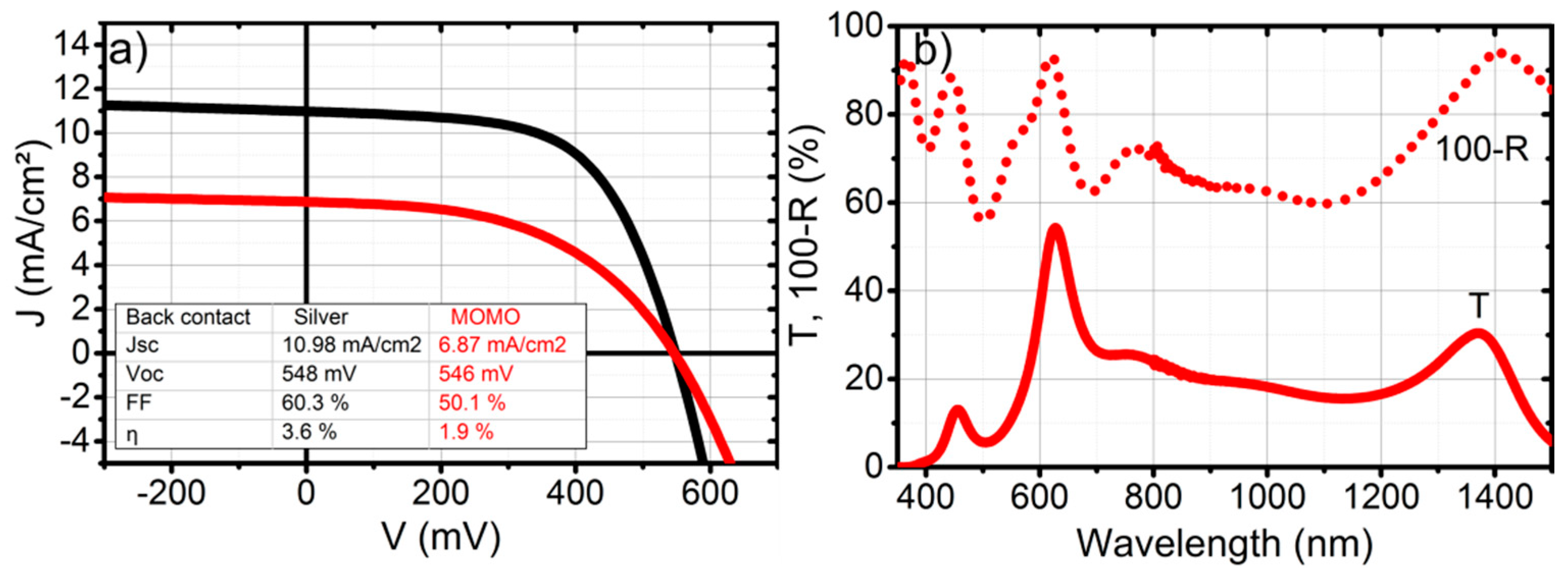
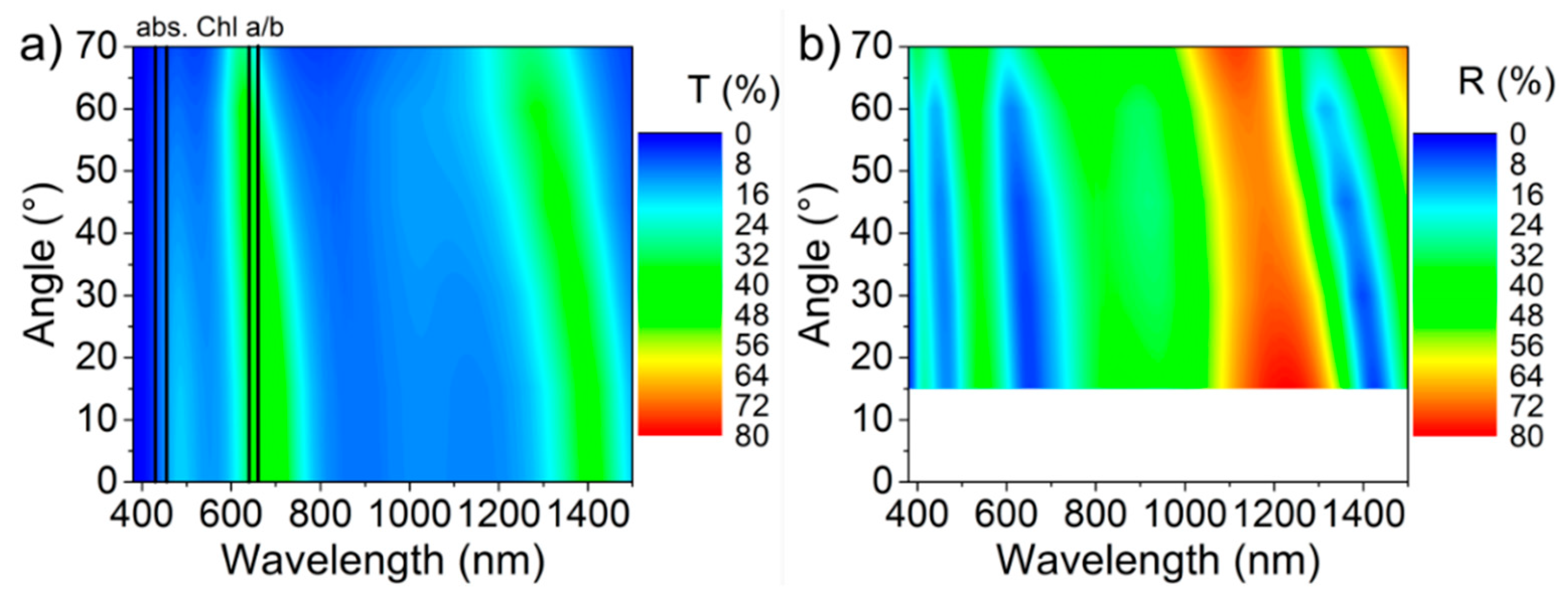
5. Spectrally Selective Solar Cells
6. Conclusions
Author Contributions
Funding
Acknowledgments
Conflicts of Interest
References
- Shah, A.V.; Schade, H.; Vanecek, M.; Meier, J.; Vallat-Sauvain, E.; Wyrsch, N.; Kroll, U.; Droz, C.; Bailat, J. Thin-film silicon solar cell technology. Prog. Photovolt. 2004, 12, 113–142. [Google Scholar] [CrossRef]
- Scheer, R.; Schock, H.-W. Chalcogenide Photovoltaics; Wiley-VCH: Weinheim, Germany, 2011. [Google Scholar]
- Unlu, M.S.; Strite, S. Resonant-cavity enhanced photonic devices. J. Appl. Phys. 1995, 78, 607–639. [Google Scholar] [CrossRef]
- Callahan, D.M.; Munday, J.N.; Atwater, H.A. Solar cell light trapping beyond the ray optic limit. Nano Lett. 2012, 12, 214–218. [Google Scholar] [CrossRef] [PubMed]
- Steenhoff, V.; Juilfs, M.; Ravekes, R.E.; Ahrlich, M.; Kellermann, M.; Siepmann, O.; Vehse, M.; Agert, C. Optimized optical field profile in resonant-cavity-enhanced a-Ge:H nanoabsorber solar cells for tandem cell application. IEEE J. Photovolt. 2017, 7, 3–10. [Google Scholar] [CrossRef]
- Steenhoff, V.; Theuring, M.; Vehse, M.; von Maydell, K.; Agert, C. Ultrathin resonant-cavity-enhanced solar cells with amorphous germanium absorbers. Adv. Opt. Mater. 2015, 3, 182–186. [Google Scholar] [CrossRef]
- Lattyak, C.; Steenhoff, V.; Gehrke, K.; Vehse, M.; Agert, C. Two-dimensional absorbers for solar windows: A simulation. Z. für Nat. A 2019, 74, 683–688. [Google Scholar] [CrossRef]
- Furchi, M.; Urich, A.; Pospischil, A.; Lilley, G.; Unterrainer, K.; Detz, H.; Klang, P.; Andrews, A.M.; Schrenk, W.; Strasser, G.; et al. Microcavity-integrated graphene photodetector. Nano Lett. 2012, 12, 2773–2777. [Google Scholar] [CrossRef]
- Liang, S.; Ma, Z.; Wu, G.; Wei, N.; Huang, L.; Huang, H.; Liu, H.; Wang, S.; Peng, L.M. Microcavity-integrated carbon nanotube photodetectors. ACS Nano 2016, 10, 6963–6971. [Google Scholar] [CrossRef]
- Sreekanth, K.V.; ElKabbash, M.; Caligiuri, V.; Singh, R.; De Luca, A.; Strangi, G. Realization of Point-of-Darkness and Extreme Phase Singularity in Nanophotonic Cavities. In New Directions in Thin Film Nanophotonics; Springer: Singapore, 2019; pp. 29–44. [Google Scholar]
- Li, Z.Y.; Butun, S.; Aydin, K. Large-area, lithography-free super absorbers and color filters at visible frequencies using ultrathin metallic films. ACS Photonics 2015, 2, 183–188. [Google Scholar] [CrossRef]
- Park, C.S.; Shrestha, V.R.; Lee, S.S.; Choi, D.Y. Trans-reflective color filters based on a phase compensated etalon enabling adjustable color saturation. Sci. Rep. 2016, 6, 25496. [Google Scholar] [CrossRef]
- Steenhoff, V.; Neumuller, A.; Sergeev, O.; Vehse, M.; Agert, C. Integration of a-Ge:H nanocavity solar cells in tandem devices. Sol. Energ. Mat. Sol. C. 2016, 145, 148–153. [Google Scholar] [CrossRef]
- Wang, Y.X.; Shen, P.; Liu, J.S.; Xue, Y.R.; Wang, Y.F.; Yao, M.N.; Shen, L. Recent advances of organic solar cells with optical microcavities. Sol. RRL 2019, 3, 1900181. [Google Scholar] [CrossRef]
- Lee, K.T.; Lee, J.Y.; Seo, S.Y.; Guo, L.J. Colored ultrathin hybrid photovoltaics with high quantum efficiency. Light: Sci. Appl. 2014, 3, e215. [Google Scholar] [CrossRef]
- Steenhoff, V.; Osterthun, N.; Gehrke, K.; Vehse, M.; Agert, C. Nanoabsorbers for PV New Potential Applications. In Proceedings of the 35th European Photovoltaic Solar Energy Conference and Exhibition, Brussels, Belgium, 24–28 September 2018; pp. 51–54. [Google Scholar]
- Kats, M.A.; Blanchard, R.; Genevet, P.; Capasso, F. Nanometre optical coatings based on strong interference effects in highly absorbing media. Nat. Mater. 2013, 12, 20–24. [Google Scholar] [CrossRef]
- Kats, M.A.; Sharma, D.; Lin, J.; Genevet, P.; Blanchard, R.; Yang, Z.; Qazilbash, M.M.; Basov, D.N.; Ramanathan, S.; Capasso, F. Ultra-thin perfect absorber employing a tunable phase change material. Appl. Phys. Lett. 2012, 101, 221101. [Google Scholar] [CrossRef]
- Yim, C.Y.; O’Brien, M.; McEvoy, N.; Winters, S.; Mirza, I.; Lunney, J.G.; Duesberg, G.S. Investigation of the optical properties of MoS2 thin films using spectroscopic ellipsometry. Appl. Phys. Lett. 2014, 104, 103114. [Google Scholar] [CrossRef]
- Schinke, C.; Peest, P.C.; Schmidt, J.; Brendel, R.; Bothe, K.; Vogt, M.R.; Kroger, I.; Winter, S.; Schirmacher, A.; Lim, S.; et al. Uncertainty analysis for the coefficient of band-To-Band absorption of crystalline silicon. AIP Adv. 2015, 5, 067168. [Google Scholar] [CrossRef]
- Leguy, A.M.A.; Hu, Y.; Campoy-Quiles, M.; Alonso, M.I.; Weber, O.J.; Azarhoosh, P.; van Schilfgaarde, M.; Weller, M.T.; Bein, T.; Nelson, J.; et al. Reversible hydration of CH3NH3PbI3in films, single crystals, and solar cells. Chem. Mater. 2015, 27, 3397–3407. [Google Scholar] [CrossRef]
- Adachi, S. Optical dispersion relations for GaP, GaAs, GaSb, InP, InAs, InSb, AlxGa1−xAs, and In1−xGaxAsyP1−y. J. Appl. Phys. 1989, 66, 6030–6040. [Google Scholar] [CrossRef]
- Nunley, T.N.; Fernando, N.S.; Samarasingha, N.; Moya, J.M.; Nelson, C.M.; Medina, A.A.; Zollner, S. Optical constants of germanium and thermally grown germanium dioxide from 0.5 to 6.6 eV via a multisample ellipsometry investigation. J. Vac. Sci. Technol. B 2016, 34. [Google Scholar] [CrossRef]
- Lattyak, C.; Ravekes, R.E.; Steenhoff, V.; Vehse, M.; Agert, C. Ultrathin resonant-cavity-enhanced amorphous germanium solar cells on ZnO honeycomb electrodes. IEEE J. Photovolt. 2018, 8, 3–7. [Google Scholar] [CrossRef]
- Steenhoff, V.; Juilfs, M.; Ravekes, R.E.; Vehse, M.; Agert, C. Resonant-cavity-enhanced a-Ge:H nanoabsorber solar cells for application in multijunction devices. Nano Energy 2016, 27, 658–663. [Google Scholar] [CrossRef]
- Osterthun, N.; Steenhoff, V.; Neugebohrn, N.; Gehrke, K.; Vehse, M.; Agert, C. Spectrally selective solar cells for simultaneous use of photosynthesis and photovoltaics. In Proceedings of the 35th European Photovoltaic Solar Energy Conference and Exhibtion, Brussels, Belgium, 24–28 September 2018; pp. 180–183. [Google Scholar]
- Osterthun, N.; Neugebohrn, N.; Gehrke, K.; Vehse, M.; Agert, C. Angle-dependent optical performance of spectrally selective solar cells for building intregrated applications. In Proceedings of the 36th European Photovoltaic Solar Energy Conference and Exhibition, Marseille, France, 9–13 September 2019; pp. 1775–1779. [Google Scholar] [CrossRef]
- Cao, D.; Xu, C.; Lu, W.Y.; Qin, C.X.; Cheng, S. Sunlight-driven photo-thermochromic smart windows. Sol. Rrl. 2018, 2, 1870163. [Google Scholar] [CrossRef]
- Kwon, H.K.; Lee, K.T.; Hur, K.; Moon, S.H.; Quasim, M.M.; Wilkinson, T.D.; Han, J.Y.; Ko, H.; Han, I.K.; Park, B.; et al. Optically switchable smart windows with integrated photovoltaic devices. Adv. Energy Mater. 2015, 5, 1401347. [Google Scholar] [CrossRef]
- Murray, J.; Ma, D.K.; Munday, J.N. Electrically controllable light trapping for self-powered switchable solar windows. ACS Photonics 2017, 4, 1–7. [Google Scholar] [CrossRef]
- Wheeler, L.M.; Moore, D.T.; Ihly, R.; Stanton, N.J.; Miller, E.M.; Tenent, R.C.; Blackburn, J.L.; Neale, N.R. Switchable photovoltaic windows enabled by reversible photothermal complex dissociation from methylammonium lead iodide. Nat. Commun. 2017, 8, 1722. [Google Scholar] [CrossRef]
- Hikmet, R.A.M.; Kemperman, H. Electrically switchable mirrors and optical components made from liquid-Crystal gels. Nature 1998, 392, 476–479. [Google Scholar] [CrossRef]
- Tajima, K.; Yamada, Y.; Bao, S.; Okada, M.; Yoshimura, K. Near colorless all-solid-state switchable mirror based on magnesium-titanium thin film. J. Appl. Phys. 2008, 103, 013512. [Google Scholar] [CrossRef]
- Tajima, K.; Yamada, Y.; Bao, S.; Okada, M.; Yoshimura, K. High durability of clear transparency all-solid-state switchable mirror based on magnesium–titanium thin film. Appl. Phys. Express 2008, 1, 067007. [Google Scholar] [CrossRef]
- Götz, M.; Lengert, M.; Osterthun, N.; Gehrke, K.; Vehse, N.; Agert, C. Switchable photocurrent generation in an ultra-thin resonant cavity solar cell. ACS Photonics 2020. under review. [Google Scholar]
- Palm, K.J.; Murray, J.B.; Narayan, T.C.; Munday, J.N. Dynamic optical properties of metal hydrides. ACS Photonics 2018, 5, 4677–4686. [Google Scholar] [CrossRef]
- Jung, H.; Cho, S.; Lee, W. A catalytic effect on hydrogen absorption kinetics in Pd/Ti/Mg/Ti multilayer thin films. J. Alloy Compd. 2015, 635, 203–206. [Google Scholar] [CrossRef]
- Yu, C.; Xu, S.Z.; Yao, J.X.; Han, S.W. Recent advances in and new perspectives on crystalline silicon solar cells with carrier-selective passivation contacts. Crystals 2018, 8, 430. [Google Scholar] [CrossRef]
- Goetzberger, A.; Zastrow, A. On the coexistence of solar-energy conversion and plant cultivation. Int. J. Sol. Energy 1982, 1, 55–69. [Google Scholar] [CrossRef]
- Dupraz, C.; Marrou, H.; Talbot, G.; Dufour, L.; Nogier, A.; Ferard, Y. Combining solar photovoltaic panels and food crops for optimising land use: Towards new agrivoltaic schemes. Renew. Energy 2011, 36, 2725–2732. [Google Scholar] [CrossRef]
- Weselek, A.; Ehmann, A.; Zikeli, S.; Lewandowski, I.; Schindele, S.; Högy, P. Agrophotovoltaic systems: Applications, challenges, and opportunities. A review. Agron. Sustain. Dev. 2019, 39. [Google Scholar] [CrossRef]
- Elamri, Y.; Cheviron, B.; Lopez, J.-M.; Dejean, C.; Belaud, G. Water budget and crop modelling for agrivoltaic systems: Application to irrigated lettuces. Agric. Water Manag. 2018, 208, 440–453. [Google Scholar] [CrossRef]
- Marrou, H.; Dufour, L.; Wery, J. How does a shelter of solar panels influence water flows in a soil–crop system? Eur. J. Agron. 2013, 50, 38–51. [Google Scholar] [CrossRef]
- Loik, M.E.; Carter, S.A.; Alers, G.; Wade, C.E.; Shugar, D.; Corrado, C.; Jokerst, D.; Kitayama, C. Wavelength-selective solar photovoltaic systems: Powering greenhouses for plant growth at the food-energy-water nexus. Earth’s Future 2017, 5, 1044–1053. [Google Scholar] [CrossRef]
- Allardyce, C.S.; Fankhauser, C.; Zakeeruddin, S.M.; Grätzel, M.; Dyson, P.J. The influence of greenhouse-Integrated photovoltaics on crop production. Solar Energy 2017, 155, 517–522. [Google Scholar] [CrossRef]
- Shi, H.; Xia, R.; Zhang, G.; Yip, H.-L.; Cao, Y. Spectral engineering of semitransparent polymer solar cells for greenhouse applications. Adv. Energy Mater. 2019, 9, 1803438. [Google Scholar] [CrossRef]
- Lichtenthaler, H.K.; Buschmann, C. Chlorophylls and carotenoids: Measurement and characterization by UV-VIS spectroscopy. Curr. Protoc. Food Anal. Chem. 2001, 1, F4. 3.1–F4. 3.8. [Google Scholar] [CrossRef]
- Heldt, H.-W.; Piechulla, B. Plant Biochemistry, 4th ed.; Academic Press: London, UK, 2010; pp. 47–48. [Google Scholar]
- Helfreich, S. Absorption spectrum of chlorophyll a and chlorophyll b. Graph, posted 19 May 2018. Available online: https://commons.wikimedia.org/wiki/File:Chlorophyll_Absorption_Spectrum.svg (accessed on 28 February 2020).
- Detweiler, A.M.; Mioni, C.E.; Hellier, K.L.; Allen, J.J.; Carter, S.A.; Bebout, B.M.; Fleming, E.E.; Corrado, C.; Prufert-Bebout, L.E. Evaluation of wavelength selective photovoltaic panels on microalgae growth and photosynthetic efficiency. Algal Res. 2015, 9, 170–177. [Google Scholar] [CrossRef]
- Lee, K.T.; Han, S.Y.; Li, Z.; Baac, H.W.; Park, H.J. Flexible high-color-purity structural color filters based on a higher-order optical resonance suppression. Sci. Rep. 2019, 9, 14917. [Google Scholar] [CrossRef]
- Allen, T.G.; Bullock, J.; Yang, X.; Javey, A.; De Wolf, S. Passivating contacts for crystalline silicon solar cells. Nat. Energy 2019, 4, 914–928. [Google Scholar] [CrossRef]
- Duell, M.; Ebert, M.; Muller, M.; Li, B.; Koch, M.; Christian, T.; Perdichizzi, R.F.; Marion, B.; Kurtz, S.; Doble, D.M. Impact of structured glass on light transmission, temperature and power of PV modules. In Proceedings of the 25th European Photovoltaic Solar Energy Conference and Exhibition, Valencia, Spain, 6–10 September 2010; pp. 3867–3872. [Google Scholar]
- Chee, K.W.A.; Tang, Z.; Lü, H.; Huang, F. Anti-Reflective structures for photovoltaics: Numerical and experimental design. Energy Rep. 2018, 4, 266–273. [Google Scholar] [CrossRef]


| Layer | Chamber | Pressure (mbar) | Power (W) | SiH4 (sccm) | GeH4 (sccm) | H2 (sccm) | B2H6 (sccm) | PH3 (sccm) | Time (s) |
|---|---|---|---|---|---|---|---|---|---|
| n a-Si | 3 | 4 | 70 | 20 | – | 450 | – | 18 | 48 |
| i a-Si | 3 | 4 | 70 | 34.7 | – | 300 | – | – | 26 |
| i a-Ge | 2 | 1.5 | 750 | 6 | 286 | – | – | x | |
| i µc-Si | 1 | 11 | 450 | 20.4 | – | 2000 | – | – | 14 |
| p µc-Si | 1 | 10 | 700 | 6 | – | 2000 | 4 | – | 42 |
| Hydrogen passivation | 1,2,3 | 4 | 70 | – | – | 600 | – | – | 60 |
| Process Parameter | Ag | AZO |
|---|---|---|
| Power [kW] | 0.2 | 1 |
| Pressure [mBar] | 8 × 10⁻³ | 6 × 10⁻³ |
| Distance target-substrate [mm] | 70 | 75 |
| Gas flow Ar/O2 [sccm] | 60/– | 100/10 |
| Deposition rate [nm/s] | 1 | 1.45 |
| Material | Voltage (kV) | Current (mA) | Rate (nm/s) |
|---|---|---|---|
| Ag | 8 | 35 | 1 |
| Mg | 6 | 2.9 | 0.5 |
| Pd | 8 | 49 | 0.05 |
| MoOx | 6 | 5.5 | 0.03 |
© 2020 by the authors. Licensee MDPI, Basel, Switzerland. This article is an open access article distributed under the terms and conditions of the Creative Commons Attribution (CC BY) license (http://creativecommons.org/licenses/by/4.0/).
Share and Cite
Götz, M.; Osterthun, N.; Gehrke, K.; Vehse, M.; Agert, C. Ultrathin Nano-Absorbers in Photovoltaics: Prospects and Innovative Applications. Coatings 2020, 10, 218. https://doi.org/10.3390/coatings10030218
Götz M, Osterthun N, Gehrke K, Vehse M, Agert C. Ultrathin Nano-Absorbers in Photovoltaics: Prospects and Innovative Applications. Coatings. 2020; 10(3):218. https://doi.org/10.3390/coatings10030218
Chicago/Turabian StyleGötz, Maximilian, Norbert Osterthun, Kai Gehrke, Martin Vehse, and Carsten Agert. 2020. "Ultrathin Nano-Absorbers in Photovoltaics: Prospects and Innovative Applications" Coatings 10, no. 3: 218. https://doi.org/10.3390/coatings10030218
APA StyleGötz, M., Osterthun, N., Gehrke, K., Vehse, M., & Agert, C. (2020). Ultrathin Nano-Absorbers in Photovoltaics: Prospects and Innovative Applications. Coatings, 10(3), 218. https://doi.org/10.3390/coatings10030218