Characterization and Wear Response of Magnetron Sputtered W–B and W–Ti–B Coatings on WC–Co Tools


Abstract
1. Introduction
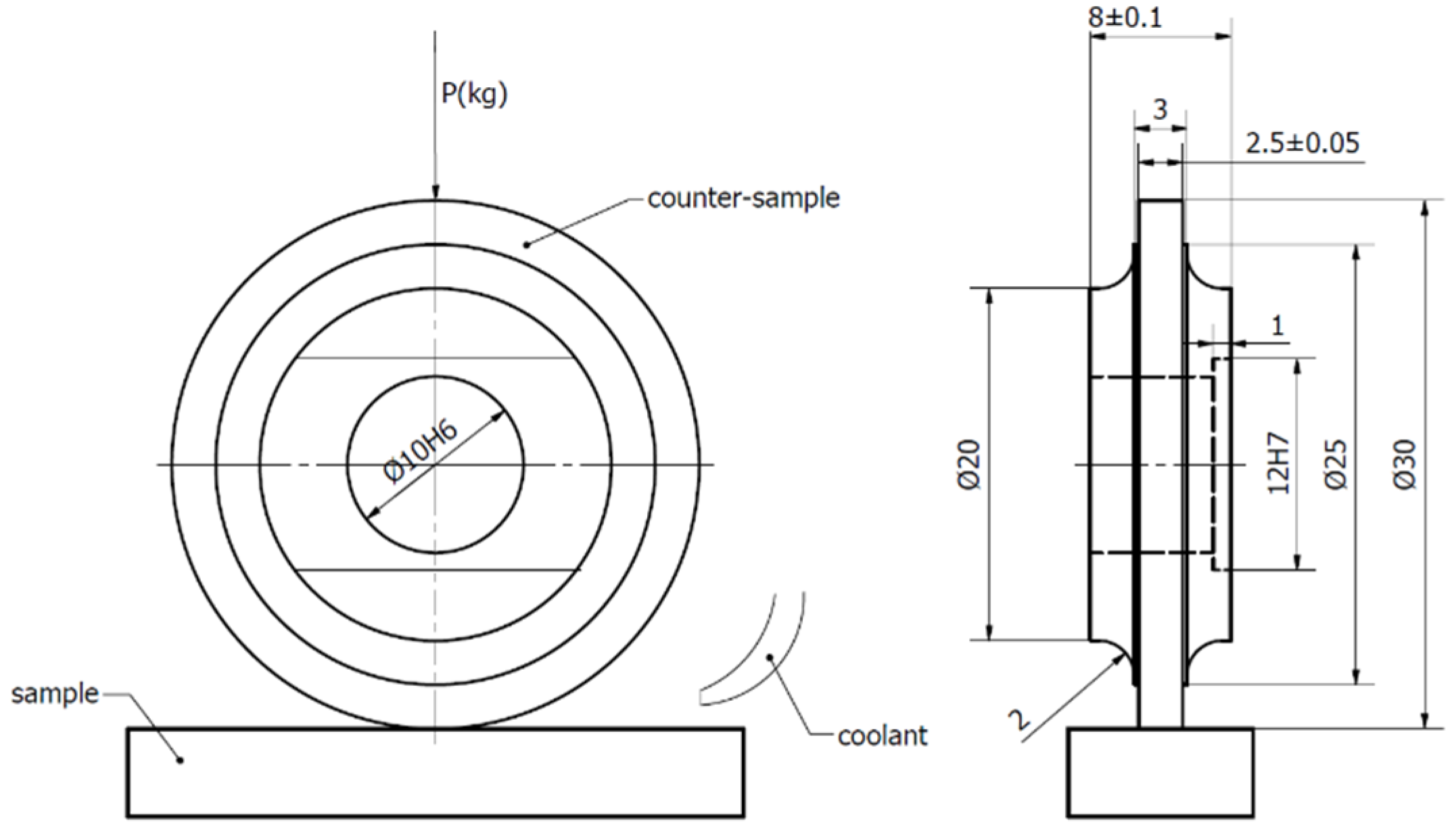
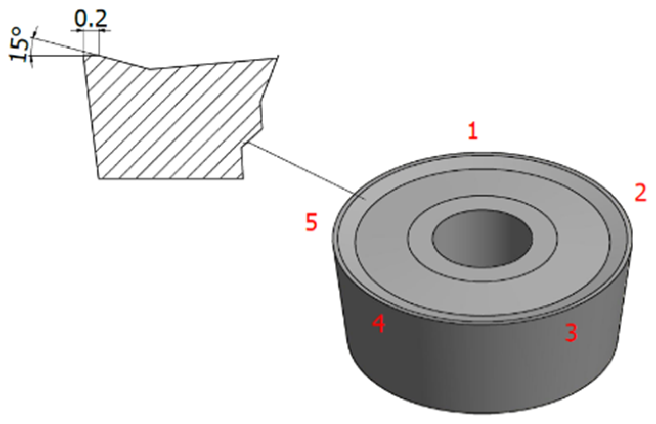
2. Experimental Procedure
3. Results and Discussion
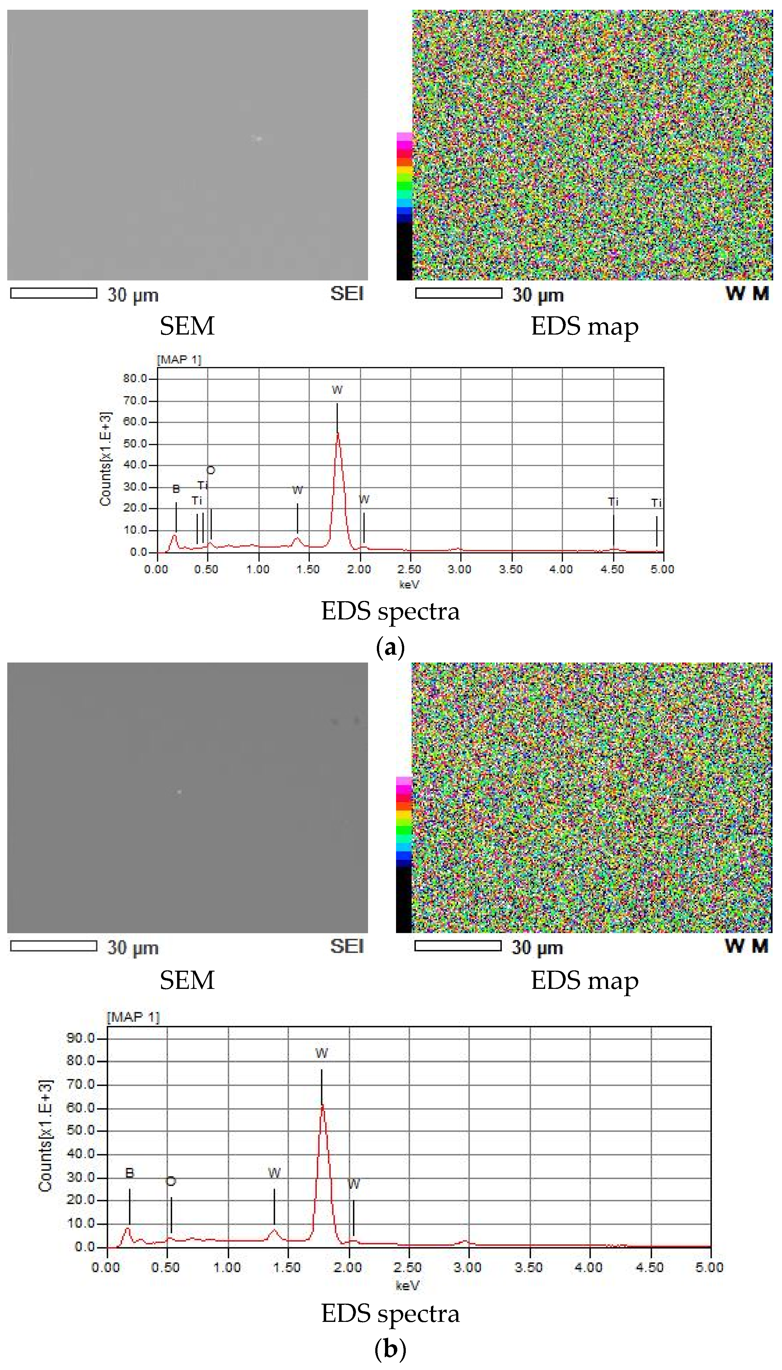
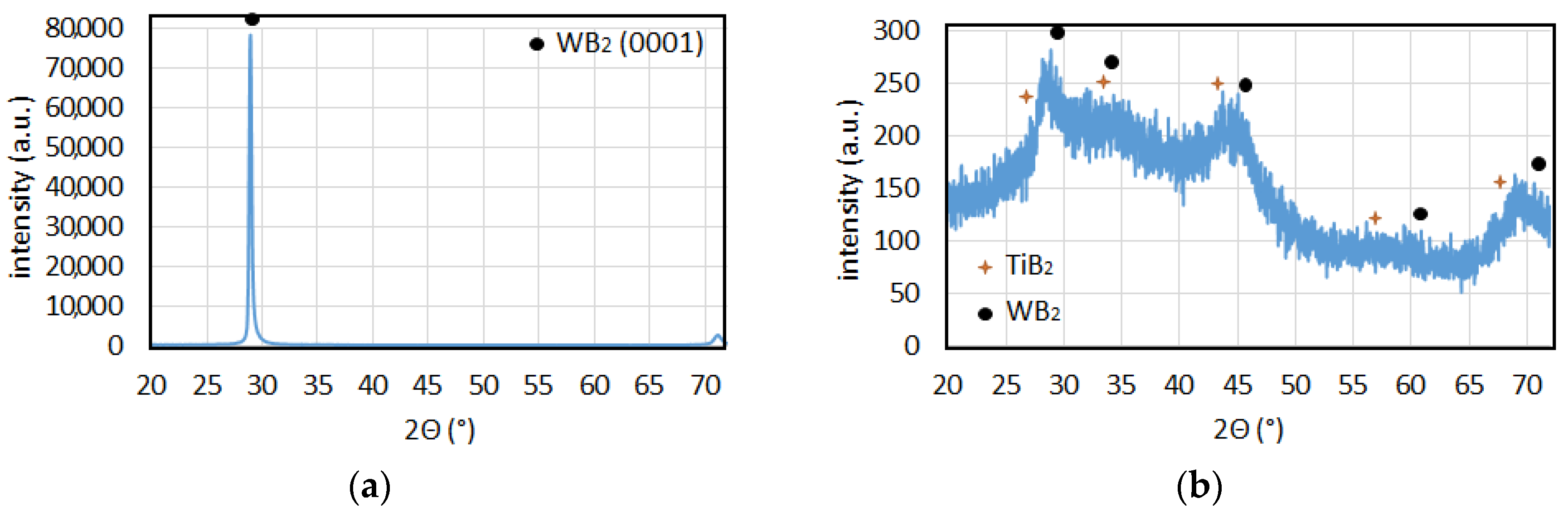
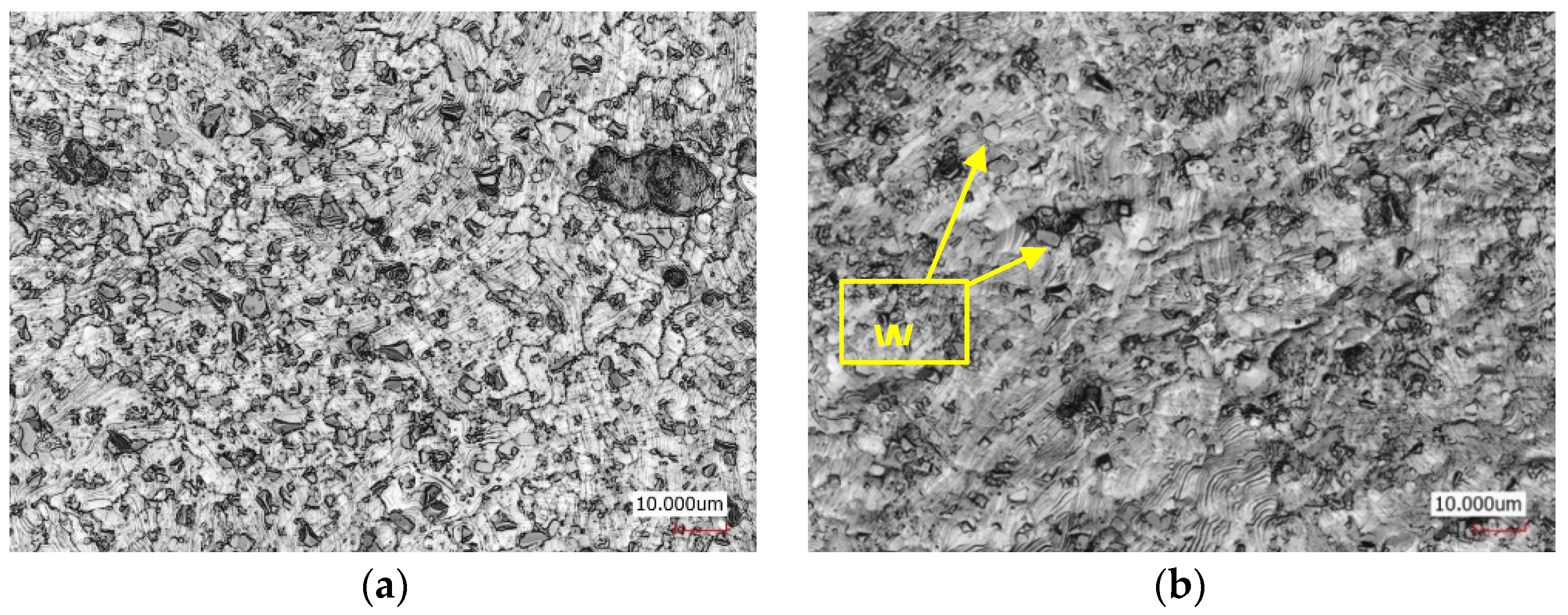
3.1. Microstructure
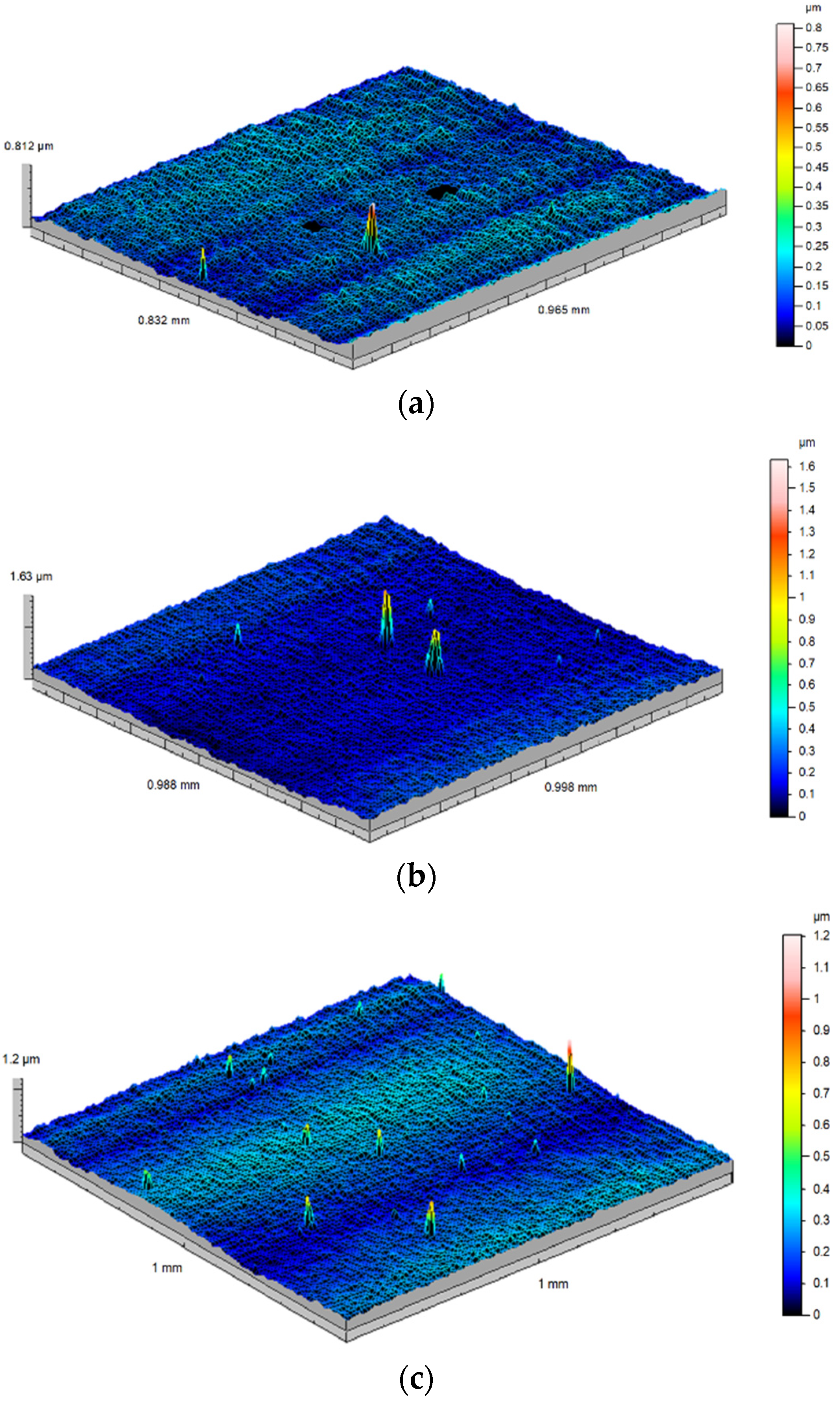
3.2. Surface Topography
3.3. Microhardness
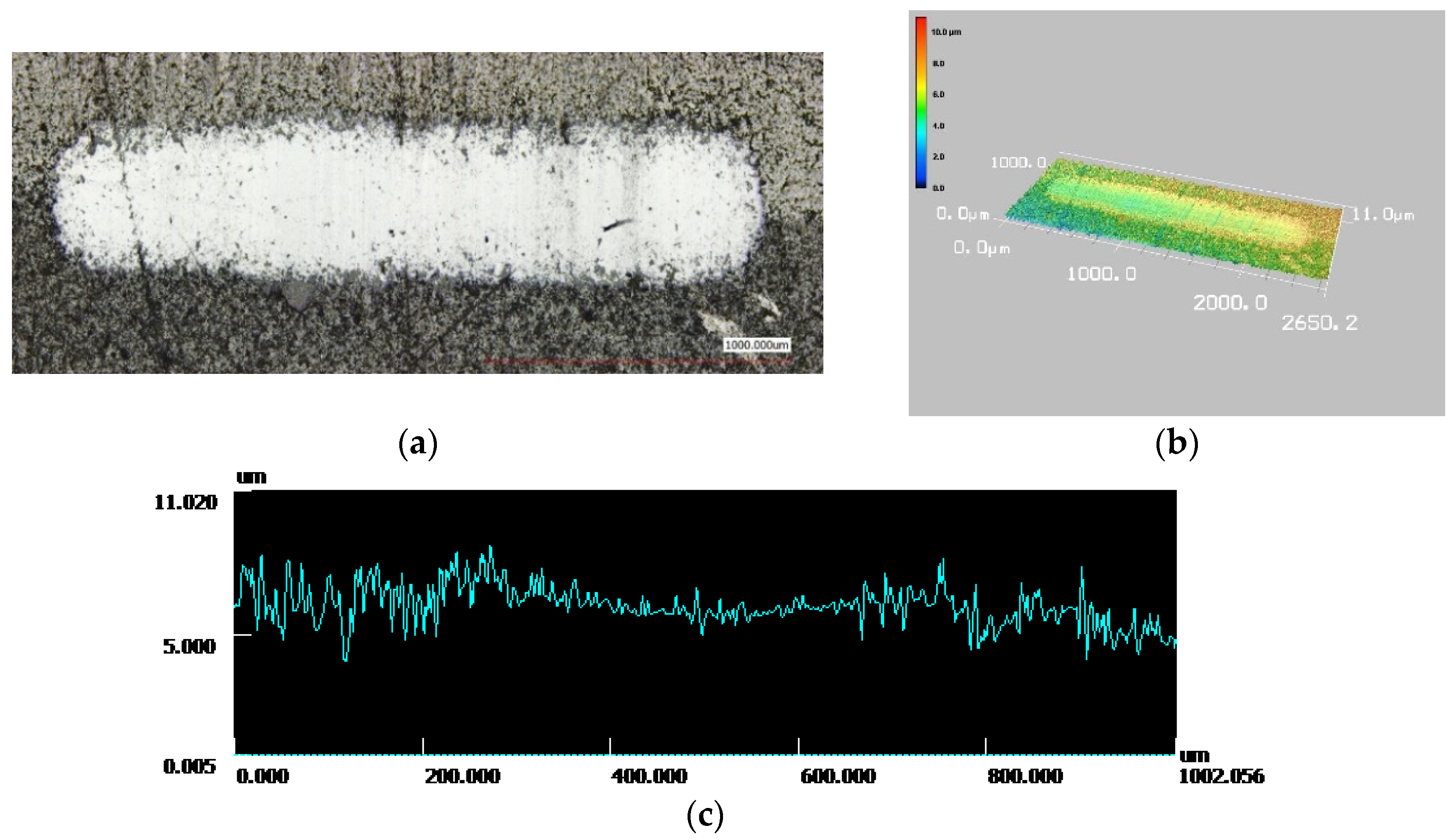
3.4. Wear Test
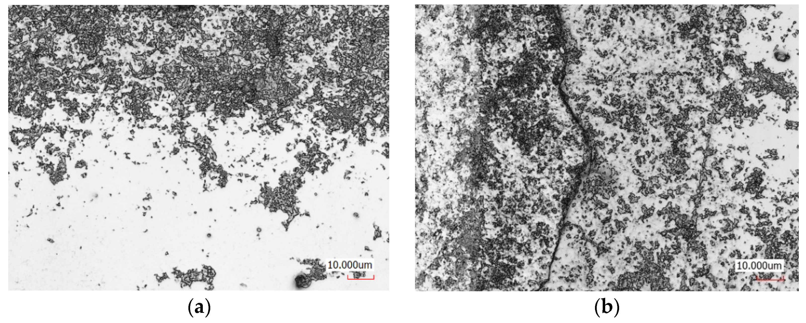
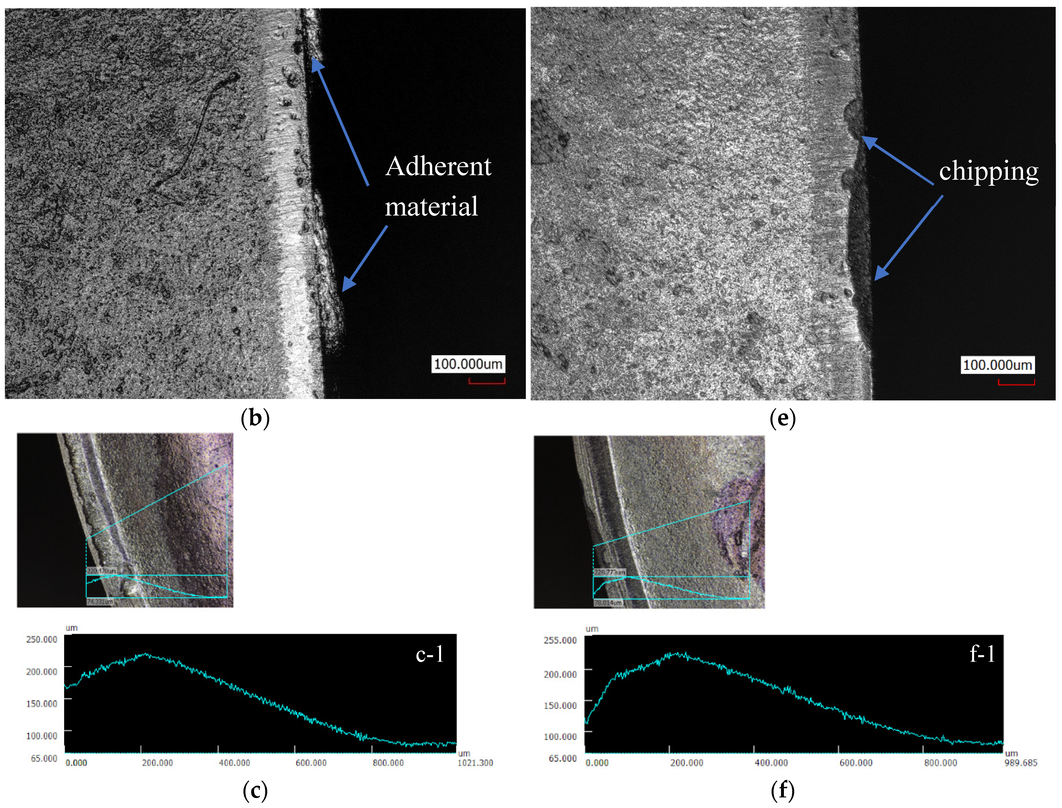
3.5. Turning Test
4. Conclusions
- W–B and W–Ti–B coatings deposited on WC–Co substrate are smooth and very hard. However, titanium alloy films with hardness of 3630 ± 260 HV0.02 are characterized by lower adhesion to the substrate, which influences the wear mechanism.
- The wear test at semi-dry sliding friction revealed 40% better wear resistance for W–B coating compared to WC–Co and W–Ti–B coating. In case of the W–Ti–B film, delamination and cracking were noted.
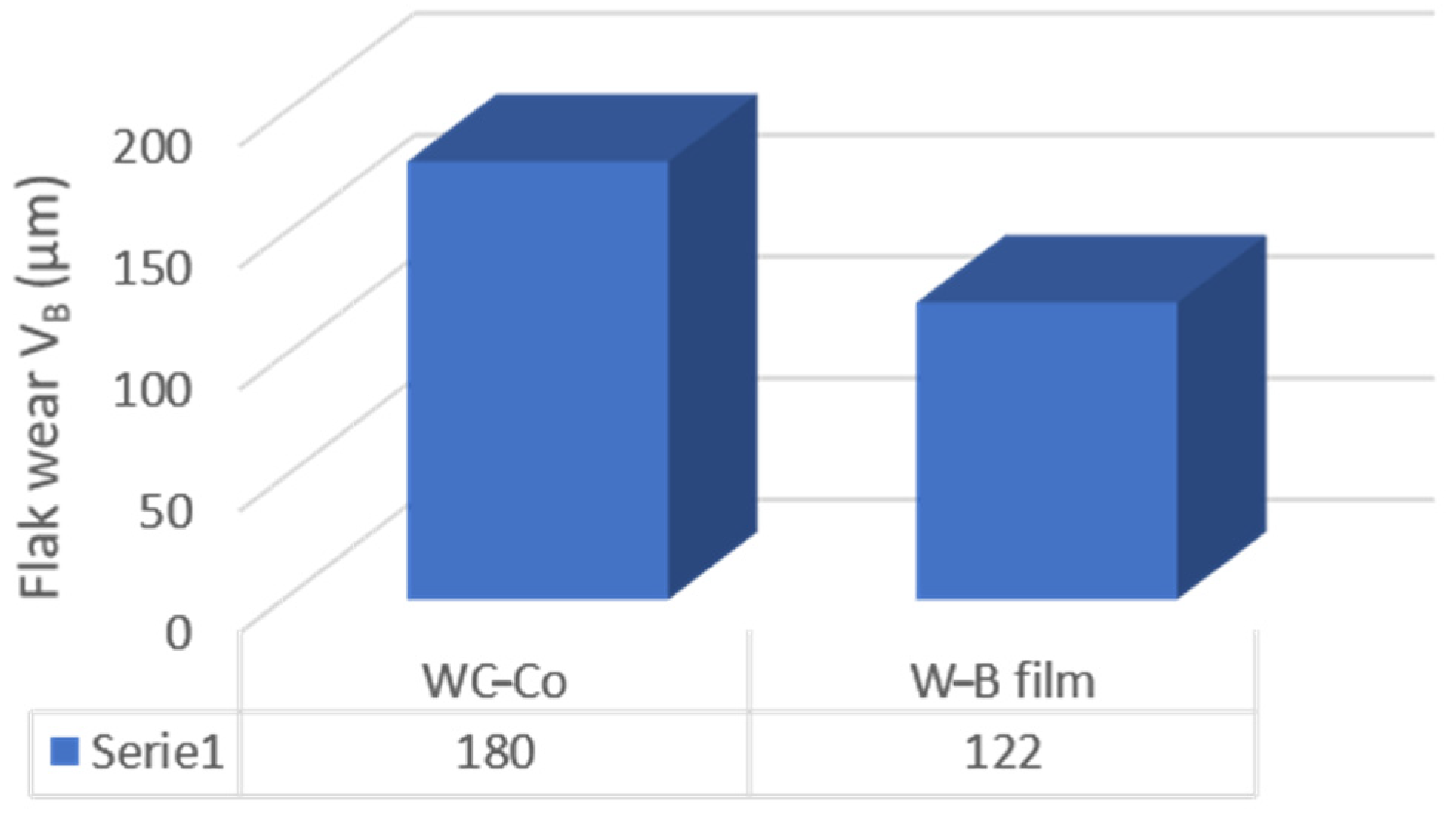
- In the turning test of difficult-to-cut 304 stainless steel, the W–B coated tool showed better wear resistance than the uncoated tool.
- Flank wear was smaller by 30% when W–B film was applied, compared to uncoated WC–Co insert. Additionally, coating prevented chipping of the edge during cutting in tested conditions.
- W–B film deposited by magnetron sputtering has great potential as a coating for cutting tools for difficult-to-cut materials, but it is necessary to carry out more tests under various cutting conditions.
Author Contributions
Funding
Conflicts of Interest
References
- Yumashev, A. Mikhaylov Development of polymer film coatings with high adhesion to steel alloys and high wear resistance. Polym. Compos. 2020, 41, 2875–2880. [Google Scholar] [CrossRef]
- Fuger, C.; Moraes, V.; Hahn, R.; Bolvardi, H.; Polcik, P.; Riedl, H.; Mayrhofer, P.H. Influence of Tantalum on phase stability and mechanical properties of WB2. MRS Commun. 2019, 9, 375–380. [Google Scholar] [CrossRef]
- Alishahi, M.; Mirzaei, S.; Souček, P.; Zábranský, L.; Buršíková, V.; Stupavská, M.; Peřina, V.; Balázsi, K.; Czigány, Z.; Vašina, P. Evolution of structure and mechanical properties of hard yet fracture W–B–C coatings with varying C/W ratio. Surf. Coat. Technol. 2018, 340, 103–111. [Google Scholar] [CrossRef]
- Moscicki, T.; Psiuk, R.; Slominska, H.; Levintant-Zayonts, N.; Garbiec, D.; Pisarek, M.; Bazarnik, P.; Nosewicz, S.; Chrzanowska-Giżyńska, J. Influence of overstoichiometric boron and titanium addition on the properties of RF magnetron sputtered tungsten borides. Surf. Coat. Technol. 2020, 390, 125689. [Google Scholar] [CrossRef]
- Chrzanowska, J.; Hoffman, J.; Denis, P.; Giżyński, M.; Mościcki, T. The effect of process parameters on rhenium diboride films deposited by PLD. Surf. Coat. Technol. 2015, 277, 15–22. [Google Scholar] [CrossRef]
- Wicher, B.; Chodun, R.; Trzciński, M.; Lachowski, A.; Kubiś, M.; Nowakowska-Langier, K.; Zdunek, K. Design of pulsed neon injection in the synthesis of W–B–C films using magnetron sputtering from a surface-sintered single powder cathode. Thin Solid Film. 2020, 716, 138426. [Google Scholar] [CrossRef]
- Berger, M.; Coronel, E.; Olsson, E. Microstructure of d.c. magnetron sputtered TiB2 coatings. Surf. Coat. Technol. 2004, 185, 240–244. [Google Scholar] [CrossRef]
- Pierson, J.; Belmonte, T.; Michel, H. Low temperature growth mechanisms of zirconium diboride films synthesised in flowing microwave Ar–BCl3 post discharges. Surf. Coat. Technol. 1999, 116–119, 1049–1054. [Google Scholar] [CrossRef]
- Dearnley, P.; Schellewald, M.; Dahma, K. Characterisation and wear response of metal-boride coated WC–Co. Wear 2005, 259, 861–869. [Google Scholar] [CrossRef]
- Chrzanowska-Giżyńska, J.; Denis, P.; Woźniacka, S.; Kurpaska, Ł. Mechanical properties and thermal stability of tungsten boride films deposited by radio frequency magnetron sputtering. Ceram. Int. 2018, 44, 19603–19611. [Google Scholar] [CrossRef]
- Chrzanowska, J.; Kurpaska, Ł.; Giżyński, M.; Hoffman, J.; Szymański, Z.; Mościcki, T. Fabrication and characterization of superhard tungsten boride layers. Ceram. Int. 2016, 42, 12221–12230. [Google Scholar] [CrossRef]
- Jiang, C.; Pei, Z.; Liu, Y.; Xiao, J.; Gong, J.; Sun, C. Preparation and characterizationof superhard AlB2-type WB2 nanocomposite coatings. Phys. Status Solidi A 2013, 210, 1221–1227. [Google Scholar] [CrossRef]
- Paiva, J.; Shalaby, M.; Chowdhury, M.; Shuster, L.; Chertovskikh, S.; Covelli, D.; Junior, E.L.; Stolf, P.; Elfizy, A.; Brok, C.S.; et al. Tribological and wear performance of carbide tools with TiB2 PVD coating under varying machining conditions of TiAl6V4 aerospace alloy. Coatings 2017, 7, 187. [Google Scholar] [CrossRef]
- Euchner, H.; Mayrhofer, P.; Riedl, H.; Klimashin, F.; Limbeck, A.; Polcik, P.; Kolozsvari, S. Solid solution hardening of vacancy stabilized TixW1−xB2. Acta Mater. 2015, 101, 55–61. [Google Scholar] [CrossRef]
- Sobol, O.; Dub, S.; Pogrebnjak, A.; Mygushchenko, R.; Postelnyk, A.; Zvyagolsky, A.; Tolmachova, G. The effect of low titanium content on the phase composition, structure, and mechanical properties of magnetron sputtered WB2–TiB2 films. Thin Solid Film. 2018, 662, 137–144. [Google Scholar] [CrossRef]
- Chrzanowska-Giżyńska, J.; Denis, P.; Giżyński, M.; Kurpaska, Ł.; Mihailescu, I.; Ristoscu, C.; Szymański, Z.; Mościcki, T. Thin WBx and WyTi1−yBx films deposited by combined magnetron sputtering and pulsed laser deposition technique. Appl. Surf. Sci. 2019, 478, 505–513. [Google Scholar] [CrossRef]
- Wang, H.; Wang, B.; Li, S.; Xue, Q.; Huang, F. Toughening magnetron sputtered TiB2 coatings by Ni addition. Surf. Coat. Technol. 2013, 232, 767–774. [Google Scholar] [CrossRef]
- Newirkowez, A.; Cappi, B.; Telle, R.; Schmidt, H. (Ti,W,Cr)B2 coatings produced by dc magnetron sputtering. Thin Solid Film. 2012, 520, 1775–1778. [Google Scholar] [CrossRef]
- Sobol, O.; Grigoryev, O.; Kunitsky, Y.; Dub, S.; Podtelezhnikov, A.; Stetsenko, A. Peculiarities of structure state and mechanical characteristics in ion-plasma condensates of quasibinary system borides W2B5–TiB2. Sci. Sinter. 2006, 38, 63–72. [Google Scholar] [CrossRef]
- Smolik, J.; Kacprzńska-Gołacka, J.; Sowa, S.; Piasek, A. The analysis of resistance to brittle cracking of tungsten doped TiB2 coatings obtained by magnetron sputtering. Coatings 2020, 10, 807. [Google Scholar] [CrossRef]
- Smolik, J.; Mazurkiewicz, A.; Garbacz, H.; Kopia, A. Tungsten doped TiB2 coatings obtained by magnetron sputtering. J. Mach. Constr. Maint. 2018, 4, 27–32. [Google Scholar]
- Musil, J. Flexible hard nanocomposite coatings. RSC Adv. 2015, 5, 60482–60495. [Google Scholar] [CrossRef]
- Moscicki, T.; Radziejewska, J.; Hoffman, J.; Chrzanowska, J.; Levintant-Zayonts, N.; Garbiec, D.; Szymanski, Z. WB2 to WB3 phase change during reactive spark plasma sintering and pulsed laser ablation/deposition processes. Ceram. Int. 2015, 41, 8273–8281. [Google Scholar] [CrossRef]
- ISO 4288 Geometrical Product Specifications (GPS)—Surface Texture: Profile Method—Rules and Procedures for the Assessment of Surface Texture; International Organization for Standardization (ISO): Geneva, Switzerland, 1 August 1996.
- ISO 11562 Geometrical Product Specifications (GPS)—Surface Texture: Profile Method—Metrological Characteristics of Phase Correct Filters; International Organization for Standardization (ISO): Geneva, Switzerland, 1 December 1996.
- T-MaxⓇ P Insert for Turning RCMX 12 04 00 H13A (SANDVIK Coromant ). Available online: https://www.sandvik.coromant.com/en-gb/products/pages/productdetails.aspx?c=rcmx%2012%2004%2000%20h13a (accessed on 15 December 2020).
- Humphrey, G.L. The heats of formation of TiO, Ti2O3, Ti3O5 and TiO2 from combustion calorimetry. J. Am. Chem. Soc. 1951, 73, 1587–1590. [Google Scholar] [CrossRef]
- Shovkoplyas, O.A.; Sobol, O.V. Influence of thermal and radiation effects on the phase composition, structure and stress-strain state of Ti–W–B system coatings deposited from ion-atomic fluxes. J. Nano-Electron. Phys. 2014, 6, 02024. [Google Scholar]
- Moraes, V.; Riedl, H.; Fuger, C.; Polcik, P.; Bolvardi, H.; Holec, D.; Mayrhofer, P. Ab initio inspired design of ternary boride thin films. Sci. Rep. 2018, 8, 9288. [Google Scholar] [CrossRef]
- Jonsson, B.; Hogmark, S. Hardness measurement of thin films. Thin Solid Film. 1984, 114, 257–269. [Google Scholar] [CrossRef]
- Zhao, F.; Tao, Q.; You, C.; Ye, M.; Li, L.; Han, Y.; Dong, S.; Wang, X.; Cui, T.; Zhu, P. Enhanced hardness in tungsten–substituted molybdenum diboride solid solutions by local symmetry reduction. Mater. Chem. Phys. 2020, 251, 123188. [Google Scholar] [CrossRef]
- Bakhit, B.; Palisatis, J.; Wu, Z.; Sortica, M.; Primetzhofer, D.; Persson, P.; Rosen, J.; Hultman, L.; Petrov, I.; Greene, J.; et al. Age hardening in superhard ZrB2-rich Zr1−xTaxBy thin films. Scr. Mater. 2021, 191, 120–125. [Google Scholar] [CrossRef]


| Composition | WBy | W1−xTixBy | ||
|---|---|---|---|---|
| Mass % | Atom % | Mass % | Atom % | |
| B | 12.0 | 67.2 | 14.1 | 68.3 |
| W | 86.9 | 28.7 | 81.1 | 23.1 |
| Ti | 0 | 0 | 3.2 | 3.5 |
| O | 1.1 | 4.1 | 1.6 | 5.1 |
| y = B/(W + Ti) | – | 2.3 | – | 2.6 |
| x = Ti/(W + Ti) | – | 0 | – | 0.1 |
| Roughness Parameters (μm) | WC | W–B | W–Ti–B |
|---|---|---|---|
| Ra | 0.022 | 0.029 | 0.038 |
| Rq | 0.026 | 0.036 | 0.043 |
| Rp | 0.069 | 0.119 | 0.096 |
| Rv | 0.066 | 0.089 | 0.090 |
| Rz | 0.134 | 0.208 | 0.145 |
| Sm | 5.4 | 6.3 | 4.5 |
| Roughness Parameters (μm) | WC | W–B | W–Ti–B |
|---|---|---|---|
| Sa | 0.026 | 0.045 | 0.043 |
| Sp | 0.667 | 1.470 | 1.010 |
| Sv | 0.144 | 0.166 | 0.208 |
| Sz | 0.809 | 0.906 | 0.925 |
| Insert | Roughness Parameters (μm) | |||
|---|---|---|---|---|
| Ra (µm) | Rz (µm) | Rq (µm) | Rv (µm) | |
| WC–Co | 0.43 | 3.00 | 0.55 | 1.46 |
| W–B | 0.32 | 2.30 | 0.41 | 1.14 |
| Sample Material | Volume of Loss Material (106 μm3) | Mean Value | ||||
|---|---|---|---|---|---|---|
| 1 | 2 | 3 | 4 | 5 | ||
| WC–Co | 1.06 | 0.941 | 1.217 | 1.089 | 0.978 | 1.057 |
| W–B film on WC–Co | 0.598 | 0.466 | 0.496 | 1.011 | 0.620 | 0.638 |
| W–Ti–B film on WC–Co | 1.106 | 0.897 | 1.276 | 1.197 | 1.820 | 1.259 |
| No Test | VB (μm) | |
|---|---|---|
| WC–Co | W–B Film | |
| 1 | 160 | 104 |
| 2 | 184 | 103 |
| 3 | 172 | 145 |
| 4 | 218 | 115 |
| 5 | 167 | 141 |
| Mean value | 180 | 122 |
| Std. dev. | 22.9 | 20.1 |
Publisher’s Note: MDPI stays neutral with regard to jurisdictional claims in published maps and institutional affiliations. |
© 2020 by the authors. Licensee MDPI, Basel, Switzerland. This article is an open access article distributed under the terms and conditions of the Creative Commons Attribution (CC BY) license (http://creativecommons.org/licenses/by/4.0/).
Share and Cite
Radziejewska, J.; Psiuk, R.; Mościcki, T. Characterization and Wear Response of Magnetron Sputtered W–B and W–Ti–B Coatings on WC–Co Tools. Coatings 2020, 10, 1231. https://doi.org/10.3390/coatings10121231
Radziejewska J, Psiuk R, Mościcki T. Characterization and Wear Response of Magnetron Sputtered W–B and W–Ti–B Coatings on WC–Co Tools. Coatings. 2020; 10(12):1231. https://doi.org/10.3390/coatings10121231
Chicago/Turabian StyleRadziejewska, Joanna, Rafał Psiuk, and Tomasz Mościcki. 2020. "Characterization and Wear Response of Magnetron Sputtered W–B and W–Ti–B Coatings on WC–Co Tools" Coatings 10, no. 12: 1231. https://doi.org/10.3390/coatings10121231
APA StyleRadziejewska, J., Psiuk, R., & Mościcki, T. (2020). Characterization and Wear Response of Magnetron Sputtered W–B and W–Ti–B Coatings on WC–Co Tools. Coatings, 10(12), 1231. https://doi.org/10.3390/coatings10121231