Article

Electrical Conductivity and Optical Properties of Nanoscale Titanium Films on Sapphire for Localized Plasmon Resonance-Based Sensors

1
Integrated Optics and Microwave Photonics Laboratory, Tomsk State University of Control Systems and Radioelectronics (TUSUR), 40 Lenin Avenue, 634050 Tomsk, Russia
2
Laboratory for Radiation and Plasma Technologies, Tomsk Polytechnic University, 30 Lenin Avenue, 634050 Tomsk, Russia
3
Laboratory of Radiophotonics, V.E. Zuev Institute of Atmospheric Optics SB RAS, 1 Academician Zuev Square, 634055 Tomsk, Russia
*
Author to whom correspondence should be addressed.
Coatings 2020, 10(12), 1165; https://doi.org/10.3390/coatings10121165
Submission received: 26 October 2020 / Revised: 26 November 2020 / Accepted: 27 November 2020 / Published: 28 November 2020
(This article belongs to the Section Thin Films)

Abstract

:
The developing area of plasmonics has led to the possibility of creating a new type of high-speed, high-sensitivity optical sensor for biological environment analysis. The functional layer of such biosensors are nanoscale films of noble metals. In this work we suggest using a thin film of titanium as a functional layer. This paper presents the results of the research on electrical and optical characteristics of 5 to 80 nm thick titanium films deposited on sapphire substrates by magnetron sputtering. It is shown that surface plasmon resonance is consistently observed in the investigated titanium films and the theoretical grounds of surface plasmon resonance excitement is given. In structures with titanium films less than 15 nm thick, local plasmon resonance is observed along with surface plasmon resonance. Local plasmon resonance is more sensitive to the surface state of a thin film of titanium, which on the one hand increases the sensitivity of a biosensor, and on the other hand imposes restrictions on the parameters of nanoscale films.

1. Introduction

There has recently been increased scientific and applied interest in surface plasmons: collective vibrations of metal conduction electrons excited by an electromagnetic wave of light radiation at the interface with a dielectric [1,2,3,4,5]. The excitement of surface plasmon resonance is accompanied by the increased luminescence of the medium, absorption of light radiation, Raman scattering, etc. One of the promising applications of systems where surface plasmon resonance is excited is optical sensors for biological medium analysis [2,3,4,5]. The prospects of optical sensors based on surface plasmon resonance are caused by their non-invasiveness, speed, high sensitivity, availability, and simplicity [2,5].
The functional metal layer of surface plasmon resonance-based optical biosensors is almost always made of nanosize films of noble metals [4,5]. The use of less precious inert metals can extend the applicability and availability of surface plasmon resonance-based biological sensors.
Titanium thin films are a promising material for the creation of biomedical sensory devices for plasmonics and radio photonics, including superconductive ones operating at terahertz frequencies [1,6]. Titanium films have unique electrical, optical, and catalytic characteristics, as well as high adhesiveness to most metallic, inorganic, and organic materials. There are practically no reports on the development of optical biosensors based on surface plasmon resonance.
The purpose of this work is to analyze the electrical and optical properties of thin titanium films deposited on sapphire substrates by magnetron sputtering for the subsequent use of the films in optical devices for plasmonics and radio photonics.

2. Materials and Methods

The technological advantage of titanium is caused by the variety of methods of obtaining its thin layers with thicknesses from tens of micrometers to single nanometers. The methods of thermal and magnetron vacuum sputtering are the most widespread. Films deposited by thermal sputtering have high electrical conductivity close to that of high purity titanium but low adhesion strength. In addition, the surface plasmon resonance of such films is shifted to the ultraviolet spectrum area, which makes their application in optical sensors more difficult [6,7,8].
The thin films of titanium described in this paper were deposited by magnetron sputtering on 650 μm thick one-sided polished sapphire substrates for LED applications (Monocrystal, Stavropol, Russia). The orientation of the polished substrate surface was C-axis (0001), with the roughness value not exceeding 0.3 nm and the roughness of its backside of 0.8 to 1.2 μm.
The deposition of nanometer layers of titanium on the substrates was carried out under the following conditions. Magnetron sputtering of a 700 mm × 100 mm × 5 mm 99.99%-pure titanium target was done using 99.99%-pure argon. Residual gas pressure in the vacuum chamber was 3 × 10⁻³ Pa. Working gas pressure was maintained at 2.5 × 10⁻³ Pa. The substrate was a distance of 10 cm from the target surface. The magnetron sputtering system was powered by a unit that generated 133 kHz impulses of direct current. Before the film deposition, the substrate surface was cleaned by an ion beam. The accelerating voltage of the closed drift ion source was 3 kV.
The adhesion of titanium films each with a thickness of 100 nm were applied to sapphire substrates according to the described technology at the level of 6 MPa.
A quartz sensor was used to control the thickness of the film while the changes in its resonance frequency were monitored by a Micron-5 meter (Izovac, Minsk, Republic of Belarus).
The control of the films’ surface relief was carried out by the means of electronic, atomic force, and scanning probe microscopy. The control of the samples’ specific resistance was carried out using a four-probe method. The optical properties were measured with a UV-2700 spectrometer (Shimadzu, Kyoto, Japan) and Ellipse 1981 SAG spectral ellipsometric complex (Institute of Semiconductor Physics, Novosibirsk, Russia).

3. Results

Using the described technology, a series of samples with thicknesses from 5 to 80 nm was produced for these studies with five pieces of each thickness value. In this study, the values of measured parameters of thin titanium films were averaged for samples of each thickness value, respectively.
The first measured parameter of the researched samples was their electrical resistivity. Figure 1 presents experimental data on how the electrical resistivity of thin films deposited by thermal (1) and magnetron (2) sputtering depends on their thickness. The electrical resistivity of films deposited by magnetron sputtering was significantly higher than that of films deposited by thermal evaporation [9]. This difference is due to the composition, defect, and structure of the films [10]. The films obtained by magnetron sputtering were solid but have a “lumpy” texture [11]. The diameter of the “bumps” in 5 to 15 nm thick films varied from several to hundreds of nm (Figure 2b), while their height did not exceed 15 nm (Figure 2b).
Numerous studies show that, at a film thickness of 1 to 10 nm, island embryos are formed, mainly of spherical shape, and they grow with the increasing thickness of a film, transforming into five-hex prisms [11,12,13,14]. It was discovered by X-ray diffraction methods that the titanium films obtained by magnetron sputtering are crystalline, regardless of the substrate material (silicon, quartz, or sapphire), and grow in the direction (0001) perpendicular to the substrate surface [13].
When analyzing optical properties, the concept of relative complex permittivity is used. The change of the imaginary part of the material’s relative permittivity (ε2), depending on the frequency (ω), along with the change of its electrical conductivity occurs in accordance with the Drude Equation [15]:
ε 2 = ε 1 4 i π c σ ω = ( 1 ω p 2 ω 2 ) ,
where ε1 is the real part of the material’s relative permittivity, c is the speed of light, σ is the electrical conductivity of titanium, i is the imaginary unit, and ωp is the plasmon resonance frequency. In this case, the second term of the Equation (1), which gives the main contribution to the imaginary part of the relative complex permittivity (absorption index), by its modulus, can significantly exceed the real part, and the relative permittivity can take negative values. A case is of interest when the plasmon resonance frequency is equal to that of laser radiation, with ε2 = 0 [16]. Plasmon resonance frequency in this case is:
ω p = ω = e N m n ε 0
where N is the concentration of free electrons, mn* is the effective mass of electrons, and ε0 is the electric constant.
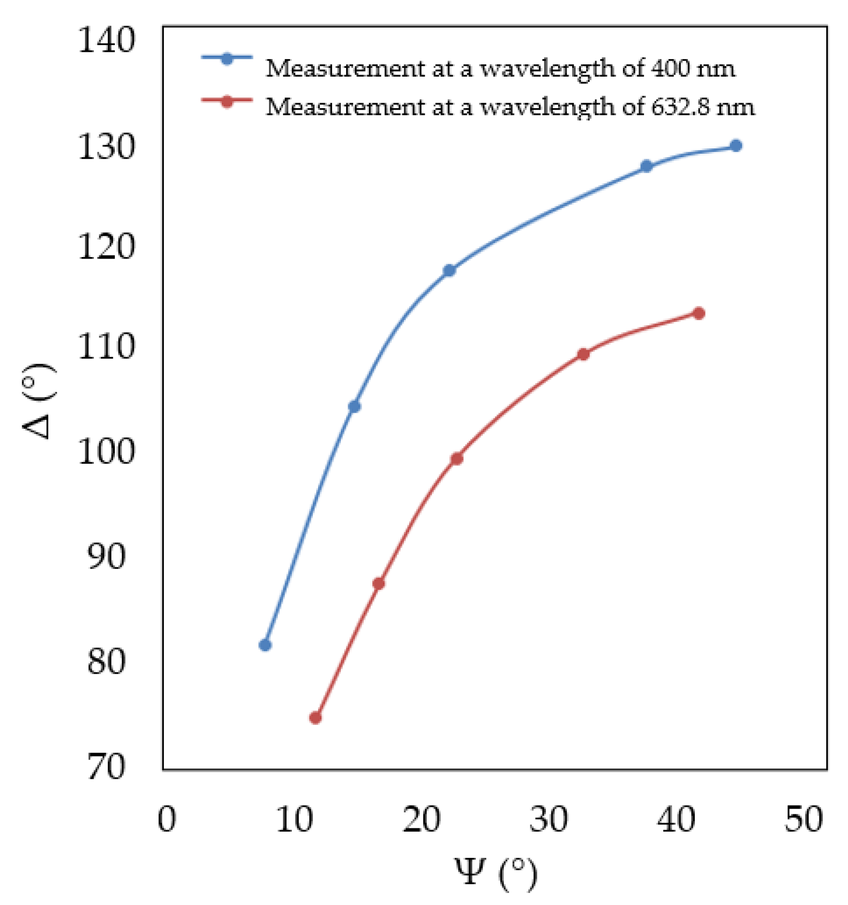
In this paper, the relative complex permittivity of films was measured in the wavelength range from 350 to 1100 nm by the means of a spectral ellipsometer: by registering the main ellipsometric parameters Ψ and Δ. As we know, these parameters carry integral information about both optical parameters and the geometry of films. The results are shown in Figure 3.
The obtained dependencies at the wavelength of 632.8 nm practically coincide with the data obtained in [17], which testifies to the reproducibility of the method for film production and similarity of technological equipment for titanium film deposition. To determine the complex refractive index, the inverse problem of ellipsometry was solved: an absorbing film on the surface of a nonabsorbing substrate with known optical characteristics. The following values for the complex refractive index (n) were obtained using this approach: n = 1.9 − 2.5i at a wavelength of 632.8 nm and n = 1.59 − 2.1i at a wavelength of 400 nm, where i is the imaginary unit.
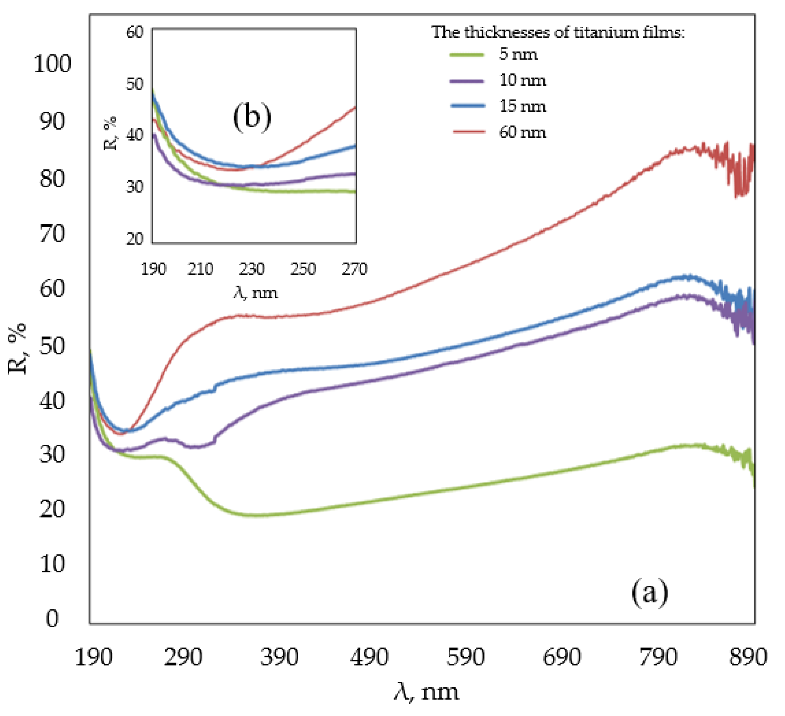
It is known that the plasmon resonance wavelength in monolithic titanium samples is 160 to 170 nm, which is in the vacuum ultraviolet. In a thin-film material, plasma resonance shifts towards longer wavelengths, in the range of 220–240 nm. To determine the wavelength of plasmon resonance in nanometer films of titanium, reflection spectra of the investigated samples were obtained (Figure 4).
The obtained reflection spectra of thin films of titanium on sapphire structures allowed the observation of surface plasmon resonance in thick films of titanium on the sapphire surface, plasmon resonance was observed at wavelengths of 230 to 240 nm, while in monolithic samples the resonance was observed at wavelengths of 160 to 170 nm, which indicates a lower concentration of conduction electrons. With decreasing thickness, the volume plasmon resonance shifted towards longer wavelengths [18,19,20].

4. Discussion

When the film thickness is less than 15 nm, a band associated with surface plasmon resonance in individual titanium “nanobumps” appeared in the reflection spectrum (Figure 4). Localized surface plasmon, in this case, was a collective electronic excitation of metallic nanoparticles smaller than the wavelength of the excitation electromagnetic radiation. It is known that the vibration frequencies of localized surface plasmon and surface plasmon are less than those of bulk plasmon by √3 and √2 times respectively [1].
The reflection and scattering of optical radiation by nanoparticles in thin films of titanium under the study can be described by means of the Mie theory [21]. The total effective section of the extinction (Cext) is determined with a formula:
C e x t = 24 π 2 R ε m 3 2 λ ( ε 2 ( ε 1 + 2 ε m ) 2 + ε 2 2 )
where εm is the real part of the dielectric constant of the substrate, ε1 and ε2 are the real and the imaginary part of the dielectric constant of the nanoparticle’s material, R is the radius of the nanoparticle, and λ is the wavelength of the falling light. Based on the ratio (1), local plasmon resonance in a particle occurs when ε1 = −2εm.
When the frequency of the external field coincided with that of the localized surface plasmon, a resonance occurred, resulting in a sharp strengthening of the field on the particle’s surface and an increase in the extinction Section (3) [22]. Since the spread of the “bumps” of the examined titanium films was quite large in size (Figure 2), the measured spectrum of local plasmon resonance (Figure 4) had a large width and covered the range of wavelengths from 290 to 700 μm. Therefore, to excite plasmon resonance in a narrow wavelength range to create highly sensitive optical biological sensors, along with the choice of the type of plasmon material and its thickness, it is necessary to further develop the technology of its deposition on the substrates to ensure optimal texture surface.

5. Conclusions

Surface plasmon resonance is consistently observed in the nanosize films of titanium. As the thickness of the film decreases, the band of test plasmon resonance shifts towards longer wavelengths. This is due to a decrease in the concentration of conduction electrons. Research of structures with thin films of titanium on sapphire substrate has shown that local plasmon resonance, along with surface plasmon resonance, is also observed in structures with titanium films of thickness less than 15 nm. Reflection spectra of structures with thin titanium film on sapphire (Figure 4) showed that local plasmon resonance is more sensitive to the surface state of a thin titanium film. However, at thicknesses at the single nanometer level, the local plasmon resonance spectrum is wider and less informative. Thus, titanium films with a thickness of 10 nm are the most promising for the creation of optical biomedical sensor devices in plasmonics.

Author Contributions

Conceptualization, S.S. and D.B.; methodology, S.S. and D.B.; validation, Y.Z.; formal analysis, S.S.; investigation, K.K. and S.S.; resources, I.Y.; data curation, Y.Z.; writing—original draft preparation, S.S.; writing—review and editing, Y.Z.; supervision, S.S.; project administration, I.Y. All authors have read and agreed to the published version of the manuscript.

Funding

The work was carried out with financial support from the Ministry of Science and Higher Education of the Russian Federation (Project name: Theoretical and experimental studies of ultra-wideband optoelectronic devices of fiber-optic information systems and microwave photonics based on photonic integrated circuits own development; Agreement No. 075-03-2020-237/1 from 5 March 2020; project number FEWM-2020-0040). The experimental results were obtained by the team from the Integrated Optics and Microwave Photonics Laboratory of the Tomsk State University of Control Systems and Radioelectronics using equipment of the “Impulse” center of collective usage (registration number 200568).

Conflicts of Interest

The authors declare no conflict of interest.

References

  1. Pompa, P.P.; Martiradonna, L.; Torre, A.D.; Sala, F.D.; Manna, L.; de Vittorio, M.; Calabi, F.; Cingolani, R.; Rinaldi, R. Metal-enhanced fluorescence of colloidal nanocrystals with nanoscale control. Nat. Nanotechnol. 2006, 1, 126–130. [Google Scholar] [CrossRef] [PubMed]
  2. Nepomnyashchaya, E.; Velichko, E.; Aksenov, E.; Bogomaz, T. Optoelectronic method for analysis of biomolecular interaction dynamics. IOP J. Phys. Conf. Ser. 2014, 541, 1–5. [Google Scholar] [CrossRef] [Green Version]
  3. Adam, P.M.; Salomon, L.M.; de Fornel, F.; Goudonnet, J.P. Determination of the spatial extension of the surface-plasmon evanescent field of a silver film with a photon scanning tunneling microscope. Phys. Rev. B 1993, 48, 268–283. [Google Scholar] [CrossRef] [PubMed]
  4. Mamichev, D.A.; Kuznetsov, I.A.; Maslova, N.E.; Zanaveskin, M.L. Optical sensors based on surface plasmon resonance for high-sensitive biochemical analysis. Mol. Med. 2012, 6, 19–27. (In Russian) [Google Scholar]
  5. Daghestani, H.N.; Day, B.W. Theory and applications of surface plasmon resonance, resonant mirror, resonant waveguide grating, and dual polarization interferometry biosensors. Sensors 2010, 10, 9630–9646. [Google Scholar] [CrossRef]
  6. Gandini, C.; Lacquaniti, C.; Monticone, E.; Portesi, C.; Rajteri, M.; Rastello, M.L.; Pasca, E.; Ventura, G. Correlation of critical temperatures and electrical properties in titanium films. Int. J. Mod. Phys. B 2003, 17, 948–952. [Google Scholar] [CrossRef]
  7. Minz, R.A.; Pal, S.S.; Chopra, A.; Bargujar, S.; Bhatnagar, R.; Sinha, R.K. Magnetron sputtering coated optical fiber probe designs for surface plasmon resonance sensor. IEEE J. Sel. Top. Quantum Electron. 2017, 23, 1–7. [Google Scholar] [CrossRef]
  8. Rakić, A.D.; Djurišić, A.B.; Elazar, J.M.; Majewski, M.L. Optical properties of metallic films for vertical-cavity optoelectronic devices. Appl. Opt. 1998, 37, 5271–5283. [Google Scholar] [CrossRef]
  9. Igasaki, Y.; Mitsuhashi, H. Crystal structures and electrical properties of titanium films evaporated in high vacuum. Thin Solid Films 1998, 5, 33–42. [Google Scholar] [CrossRef]
  10. Danilina, T.I.; Troyan, P.E.; Sakharov, Y.V.; Zhidik, Y.S. Ion-plasma methods to obtain nanostructures. Proc. TUSUR Univ. 2017, 20, 40–45. [Google Scholar] [CrossRef]
  11. Matveev, V.A.; Pleshanov, N.K.; Gerashchenko, O.V.; Bayramukov, V.Y. Complex study of titanium nano-films prepared by magnetron sputtering. J. Surf. Investig. X-ray Synchrotron Neutron Tech. 2014, 8, 991–996. [Google Scholar] [CrossRef]
  12. Dervaux, J.; Cormier, P.-A.; Moskovkin, P.; Douheret, O.; Konstantinidis, S.; Lazzaroni, R.; Lucas, S.; Snyders, R. Synthesis of nanostructured Ti thin films by combining glancing angle deposition and magnetron sputtering: A joint experimental and modeling study. Thin Solid Films 2017, 636, 644–657. [Google Scholar] [CrossRef]
  13. Smirnov, S.V.; Chistoedova, L.A.; Litvinova, V.A. Frame and properties of pellicles of tantalum obtained by a magnetron sputtering. Proc. TUSUR Univ. 2005, 4, 80–83. (In Russian) [Google Scholar]
  14. Lyahov, I.G.; Bulah, K.V.; Il’in, A.S. The investigation of the microstructure of titanium thin films for cryogenic detectors with various modes of magnetron sputtering. J. Radio Electron. 2012, 9, 1–13. (In Russian) [Google Scholar]
  15. Grosse, P. Freie Elektronen in Festkörpern; Springer: Berlin/Heidelberg, Germany, 1979; p. 296. [Google Scholar] [CrossRef]
  16. Kralkina, E.A.; Nekliudova, P.A.; Nikonov, A.M.; Vavilin, K.V.; Zadiriev, I.I. Properties of titanium coatings deposited in a magnetron discharge with ion assistance using an inductive RF discharge in a magnetic field. Appl. Phys. 2019, 4, 41–46. (In Russian) [Google Scholar]
  17. Bogolyubova, S.; Polyakova, E.; Rezvyi, R. Ellipsometric methods for control of parameters of materials and radioelectronics structures. Radio Ind. 2016, 26, 59–62. [Google Scholar] [CrossRef] [Green Version]
  18. Abelès, F. Optical properties of metallic films. Phys. Thin Films 1971, 6, 151–204. [Google Scholar] [CrossRef]
  19. Chang-Hasnain, J.C.; Harbison, J.B.; Hasnain, G.; Von Lehmen, A.C.; Florez, L.T.; Stoffel, N.G. Dynamic, polarization, and transverse mode characteristics of vertical cavity surface emitting lasers. IEEE J. Quantum Electron. 1991, 27, 1402–1409. [Google Scholar] [CrossRef]
  20. Ordal, M.A.; Long, L.L.; Bell, R.J.; Bell, S.E.; Bell, R.R.; Alexander, R.W.; Ward, C.A. Optical properties of the metals Al, Co, Cu, Au, Fe, Pb, Ni, Pd, Pt, Ag, Ti, and W in the infrared and far infrared. Appl. Opt. 1983, 22, 1099–1119. [Google Scholar] [CrossRef]
  21. Mie, G. Contributions to the optics of turbid media, particularly of colloidal metal solutions. Ann. Phys. 1908, 25, 377–445. [Google Scholar] [CrossRef]
  22. Ni, E.; Jiang, X. Microwave measurement of the permittivity for high dielectric constant materials using an extra-cavity evanescent waveguide. Rev. Sci. Instrum. 2002, 73, 3997–4002. [Google Scholar] [CrossRef]
Figure 1. The dependency of the electrical resistivity of titanium thin films, deposited by heat vaporizing [9] and by magnetron sputtering, on their thickness.
Coatings 10 01165 g001
Figure 2. An electron-microscopic image of a 10 nm thick titanium film surface: (a) an SEM image; (b) an SPM image.
Coatings 10 01165 g002
Figure 3. A Ψ-Δ diagram for titanium films of different thicknesses (the dots on the dependencies correspond to the thicknesses of titanium films of 5 to 60 nm).
Coatings 10 01165 g003
Figure 4. (a) Reflection spectra of structures of thin titanium film on sapphire; (b) the insert shows the increased reflection spectrum for the initial wavelength range.
Coatings 10 01165 g004
Publisher’s Note: MDPI stays neutral with regard to jurisdictional claims in published maps and institutional affiliations.