Article

Two-Dimensional As/BlueP van der Waals Hetero-Structure as a Promising Photocatalyst for Water Splitting: A DFT Study

1
Faculty of Physics and Electronic Science, Hubei University, Wuhan 430062, China
2
Shenzhen Key Laboratory of Advanced Thin Films and Applications, College of Physics and Optoelectronic Engineering, Shenzhen University, Shenzhen 518060, China
*
Authors to whom correspondence should be addressed.
The authors contributed equally to this work.
Coatings 2020, 10(12), 1160; https://doi.org/10.3390/coatings10121160
Submission received: 5 November 2020 / Revised: 23 November 2020 / Accepted: 26 November 2020 / Published: 27 November 2020

Abstract

:
Constructing van der Waals (vdW) hetero-structure by stacking different two-dimensional (2D) materials has become an effective method for designing new-type and high-quality electronic and optoelectronic nano-devices. In this work, we designed a 2D As/BlueP vdW hetero-structure by stacking monolayer arsenene (As) and monolayer blue phosphorous (BlueP) vertically, which were recently implemented in experiments, and investigated its structural, electronic, and photocatalytic water splitting properties by using the standard first principles calculation method with HSE06 hybrid exchange-correlation functional. Numerical results show that the As/BlueP vdW hetero-structure is structural robust, even at room temperature. It presents semi-conducting behavior, and the conduction band minimum (CBM) and the valence band maximum (VBM) are dominated by BlueP and As, respectively. The typical type-II band alignment predicts the potential application of the hetero-structure in highly efficient optoelectronics and solar energy conversion. Moreover, the CBM and the VBM straddle the redox potentials of water in acid environment, predicting the possibility of the As/BlueP hetero-structure as a 2D photocatalyst for water splitting. When an in-plane strain is applied, the band edges and, further, the optoelectronic properties of the hetero-structure can be effectively tuned. Especially, when tensile strain is equal to 4.5%, the optical absorption spectrum is effectively broadened in a visible light region, which will largely improve its photocatalytic efficiency, although the pH value of the solution range reduction. This work provides theoretical evidence that the As/BlueP hetero-structure has potential application as a 2D photocatalyst in water splitting.

1. Introduction

With the rapid growth of society development and increasing population, the energy requirements will absolutely increase. Currently, our daily energy mostly depends on the fossil energy, which originates from a series of environment problems, like air pollution and global warming. The exploration of clean and renewable green energy is becoming increasingly important [1]. Hydrogen is considered to be the most promising clean energy, which exists in water in large quantities and has the advantages of high calorific value, zero emission of carbon dioxide, and abundant reserves [2,3]. How to decompose hydrogen from water has become a research focus in recent decades. Two dimensional (2D) materials have attracted extensive attention due to their intriguing physical and chemical properties, and they have presented numerous potential application prospects in nanoelectronics, spintronics, and optoelectronics [4,5,6,7,8,9]. Recently, exploring the photocatalytic applications of 2D semiconducting materials, especially in water splitting, has become a hot research area, and lots of theoretical and experimental works have been carried out in order to explore the photocatalytic mechanism and detect new 2D materials [10,11,12,13,14]. When sunlight with energy larger than the band gap irradiates on the 2D semiconducting materials, electrons are excited from the valence band to the conduction band to form electron-hole pairs, and hydrogen and oxygen are eventually produced by catalysis on the surface of the material. When compared to the traditional bulk optoelectronic materials, 2D semiconducting materials possess several advantages of adjustable band gap by strain engineer, short charge transfer distance, and huge surface to volume ratio, which will greatly broaden the range of absorption spectra, accelerate catalytic process, and enhance the efficiency of optical absorption [15,16,17,18]. However, the finite thickness of 2D material is also a double-edged sword, because most of the photo-generated electrons and holes are scattered among the same surface, which enhances electron-hole recombination probability and restricts the efficiency of redox reaction to produce H2 and O2 [19].
An effective method for overcoming this drawback of electron-hole recombination in 2D semiconducting materials is constructing multi-layer van der Waals (vdW) hetero-structures by stacking different monolayer semiconductors together. If the light induced electrons and holes can be generated at different layers of the hetero-structure, the probability of electron-hole recombination can be largely reduced and the catalytic efficiency will be enhanced enormously. In general, an efficient photocatalyst of 2D semiconducting hetero-structure should possess several criteria. (1) The structure should be stable at room temperature and even under stress and electric field. (2) The optimum band alignment mode of the different layers should be type-II, which is “straggered” type can effectively ensure the photo-generated electrons and holes in different layers. Moreover, the build-in electric field between different layers can drive the electrons and holes transfer along the opposite directions in order to further reduce their recombination. (3) The band gap should be larger than 1.23 eV, which is the energy difference of oxidation and reduction potentials of water splitting, and the band edges should straddle the redox potentials to ensure the coincident and repetitive occurrence of oxidation reaction and reduction reaction.
Blue phosphorous (BlueP) is a previously predicted group-V 2D material as an allotrope of celebrated black phosphorous (BlackP). It has been recently successfully fabricated by the molecular beam epitaxy (MBE) technique growth on the Au (111) substrate [20]. Previous researches indicated that monolayer BlueP has a hexagonal structure with favorable thermal stability as monolayer BlackP and higher carrier mobility than monolayer transition metal dichalcogenides (TMDCs) [21,22]. It is a semiconductor with an indirect band gap around 2.0–3.0 eV, and its band gap can be tuned by external strain and electric field [23]. Monolayer arsenic (As) is another group-V 2D material which also was synthesized recently [24]. Previous studies indicate that there are three feasible structures of monolayer As, i.e., puckered, planar, and buckled ones, in which the buckled one has the lowest cohesive energy. Similar to BlueP, monolayer buckled As also has a hexagonal crystal structure and it shows semiconducting behavior with an indirect band gap around 1.6–2.0 eV [25,26,27,28,29]. Tremendous attention has been received in order to explore and fabricate BlueP- and As-based hetero-structures, such as BlueP/BlackP [30], BlueP/Mg(OH)2 [31], BlueP/g-GaN [32,33], MoS2/As [34], and As/C3N [35], and their electronic properties and optoelectronic properties have been explored. In this respect, we build a 2D As/BlueP vdW hetero-structure and study its electronic and optical electronic properties from first principles level in this work. Especially, we focus on its photocatalytic property and explore its potential application in water splitting. There are several reasons for the research object and research direction of this work. First, monolayer As and monolayer BlueP both belong to group-V materials, and their similar hexagonal crystal structures are favorable in building hetero-structure. Secondly, both of the two monolayers are indirect band gap semiconductors, which can effectively restrict the photo-generated electron-hole recombination and it is an advantage for photocatalytic materials. Thirdly, and most importantly, the band gaps of monolayer As (~2.2 eV) and monolayer BlueP (~2.75 eV) are much larger than the redox potentials difference of water splitting (1.23 eV), which means that only the visible light in short wavelength region can be absorbed to participate the electron excitation. While for their hetero-structure, a type-II band alignment may be formed and the band gap will be reduced in view of the much lower work function of BlueP than As, which will increase the application possibility in order to accommodate photocatalysis extremely [36].
The remainder of this paper is organized, as follows. In Section 2, the parameters used in the first principles calculation of this work are introduced. In Section 3, the numerical results are presented, in turn, including the structural and electronic behaviors of monolayer As, monolayer BlueP, and the As/BlueP vdW hetero-structure, the optical absorption, and strain adjustment of the photocatalytic water splitting properties of the hetero-structure. Finally, Section 4 provides a summary.

2. Methods

All of the first principles calculations in this work were implemented by the Vienna ab initio Simulation Package (VASP) with the exchange-correlation interaction that was treated at the Heid-Scuseria-Ernzerhof (HSE06) level [37,38,39,40,41]. The geometric structures were fully optimized with the convergence criterion equal to 10−5 eV per atom for energy and 0.02 eV/Å for force. The plane-wave cut-off energy was set as 450 eV, and the k-grids in the first Brillouin zone was set as 5 × 5 × 1. A vacuum space of 30 Å was constructed in vertical direction of the plane in order to avoid the interaction between neighboring slabs. The DFT-D2 functional with Grimme correction was applied to consider the weak vdW interaction between the adjacent layers of the hetero-structure [42]. In addition, an ab initio molecular dynamics (AIMD) simulation was performed at 300 K for 10 ps with a time step of 1 fs in order to examine the structure stability of the hetero-structure [43].

3. Results and Discussion

In the following, we discuss, in turn, the structural, electronic, optoelectronic, and photocatalytic properties in water splitting of the As/BlueP hetero-structure in detail.

3.1. Structural and Electronic Properties of Monolayer As and BlueP

The structural and electronic properties of monolayer As and BlueP were first investigated before exploring the behavior of their hetero-structure. Figure 1a shows the buckled As, which has hexagonal lattice structure from top view and alternating double folded structure from side view. Figure 1b shows the schematic structure of monolayer BlueP, which possesses hexagonal lattice structure from top view and inclined zigzag structure from side view. The optimized lattice constants are 3.61 and 3.28 Å for monolayer As and BlueP, respectively. Figure 1c,d show the band structures of monolayer As and BlueP, respectively, which are based on HSE06 hybrid functional. Obviously, both monolayer As and BlueP possess indirect band gaps. For As, the conduction band minimum (CBM) is located between Γ and M points, and the valence band maximum (VBM) is located at Γ point with a band gap equal to 2.17 eV. For monolayer BlueP, both CBM and VBM are located between Γ and M points, and the band gap is equal to 2.75 eV. More detailed projected density of states (PDOS) to the dominant bands of the two monolayers are exhibited in Figure 1e,f. For monolayer As, both valence and conduction bands are mainly composed of the 4p orbital of As atoms. While, for monolayer BlueP, both valence and conduction bands are mostly derived from the 3p orbital of P atoms. All of these results of monolayer As and BlueP are in accordance with previous researches [33,44]. In this paper, we combine the two monolayers together by forming vertical semiconducting heterojunction to investigate its electronic and photoelectronic properties in the following.

3.2. Structural Stability of the As/BlueP Hetero-Structure

Figure 2a shows the unit cell of the As/BlueP vertical hetero-structure, which is assembled by stacking the 7 × 7 supercell of As (see the dash-curve rhombus in Figure 1a) and the 3 × 3 supercell of BlueP (see the dash-curve rhombus in Figure 1b) in the direction perpendicular to the plane. The optimized lattice constant of the As/BlueP hetero-structure is 9.54 Å, which corresponds to a shrinkage of ~3.0% for monolayer BlueP. The small rectification of lattice mismatch is acceptable when considering of the small error criterion in stacking hetero-structure. The equilibrium interlayer distance is relaxed equal to 3.54 Å, which is much larger than the bond lengths of As–P (roughly 2.3 Å), indicating a vdW, but not chemical interaction of the two layers of the As/Blue hetero-structure.
The binding energy Eb was first calculated in order to confirm the structural stability of the As/BlueP hetero-structure. Eb describes the combining possibility of different materials, which is defined as [45]
E b = E A s / B l u e P E A s E B l u e P
Here, EAs, EBlueP, and EAs/BlueP represent total energies of monolayer As, monolayer BlueP, and the As/BlueP hetero-structure, respectively. The calculated As/BlueP herero-structure binding energy is equal to −4.83 eV, which is much higher than the previously proposed C2N/BlueP (−2.59 eV) [46] and As/GaS (−0.17 eV) hetero-structures [47], implying the proper structural stability of the As/BlueP hetero-structure. Furthermore, an AIMD simulation was employed to further confirm the thermal stability of the hetero-structure at room temperature. As plotted in Figure 2b, the total energy remains at −660 eV with minor fluctuations under 300 K for 10 ps, indicating the robustness of the structure. The AIMD snapshot at 10 ps shows that there is no bond break and structural rebuild, except some tiny deviations, which further confirms the stability of the As/BlueP hetero-structure.

3.3. Electronic Properties of the As/BlueP Hetero-Structure

Figure 3 presents the electronic properties and charge distribution of the As/BlueP hetero-structure in both reciprocal space and real space. Figure 3a show the band structure and PDOS obtained based on HSE06 functional, which indicate an indirect band-gap semiconductor of the hetero-structure with a band gap that is equal to 1.78 eV. Especially, the semiconductor exhibits typical type-II band alignment, where the CBM that lies in Γ point is mainly contributed by 3p orbital of P atom, while the VBM located between Γ and M points is dominated by 4p orbital of As atom. Figure 3b displays the real space charge distribution at the VBM and CBM in order to further confirm the type-II band alignment. Obviously, the lowest-energy electrons and holes are dispersed in BlueP layer and As layer, respectively, which is in accordance with the information that is shown in Figure 3a.
Figure 3c presents the band edges and work function of both monolayers and the hetero-structure in order to understand the generation mechanism of the type-II band alignment. The calculated work functions of As and BlueP monolayer are 5.03 and 6.31 eV, respectively, which are in good agreement of previous reports [48,49]. Especially, the energy of VBM of monolayer As is between the energies of CBM and VBM of monolayer BlueP, while the energy of CBM of BlueP is between the energies of CBM and VBM of monolayer As, which indictaes the formation of type-II band alignment. The valence band offset (VBO) and conduction band offset (CBO), defined as the VBM and CBM difference between As and BlueP monolayers, are 1.27 and 0.69 eV, respectively. When stacking the two monolayers as a hetero-structure, the Fermi level is pushed up largely for the BlueP layer and then pulled down slightly for the As layer to the same value due to the interlayer coupling. Although VBO and CBO are reduced to 0.05 and 0.39 eV, respectively, the type-II band alignment maintains. Thus, the electrons can spontaneously transfer from the As layer to BlueP layer, and the holes transfer in the opposite direction. As a result, the accumulation of positive and negative charges induces a built-in electric field pointing from As layer to BlueP layer, which, in turn, hinders the charge transfer and finally reaches electrostatic balance inside the hetero-structure.
Furthermore, Figure 3d shows the electrostatic potential and plane-averaged differential charge density of the As/BlueP hetero-structure along the z-direction in order to present the build-in electric field and charge transfer. The different electronegativity of As and P atoms leads to the deeper potential of BlueP layer than As layer, and the 7.28 V potential difference induces a weak built-in electric field from As layer to BlueP layer. To more clearly see the charge transfer driven by this interlaminar electric filed, the plane-averaged electron density difference Δ ρ ( z ) were also calculated, which is defined as [50]
Δ ρ ( z ) = ρ A s ( z ) + ρ B l u e P ( z ) ρ A s / B l u e P ( z )
With ρAs(z), ρBlueP(z), and ρAs/BlueP(z) indicating the plane-averaged charge densities of monolayer As, monolayer BlueP and the hetero-structure, respectively. Positive Δρ(z) represents electron depletion, and negative Δρ(z) means electron accumulation. As plotted in the lower panel of Figure 3d, electrons transfer from the As layer and accumulate near the BlueP layer, which gives rise to the large potential drop at the interface of the hetero-structure, as shown in the upper panel of Figure 3d. As a typical semiconducting vertical hetero-structure with type-II band alignment, the As/BlueP hetero-structure has certain advantages in the field of high efficiency optoelectronics and solar energy conversion, because the photogenerated electrons and holes exist in different layers, which reduces the spontaneous recombination of photogenerated charges. The generation of electron-hole pairs is the first step, not only of the photocatalytic process of water splitting, but also of the solar energy conversion into electric current. Thus, next we study the optical absorption properties of the As/BlueP hetero-structure in order to evaluate its application prospect as a optoelectronic material. Next, we will mainly discuss the behavior and potential application in photocatalytic field of the As/BlueP hetero-structure in the later of this paper.

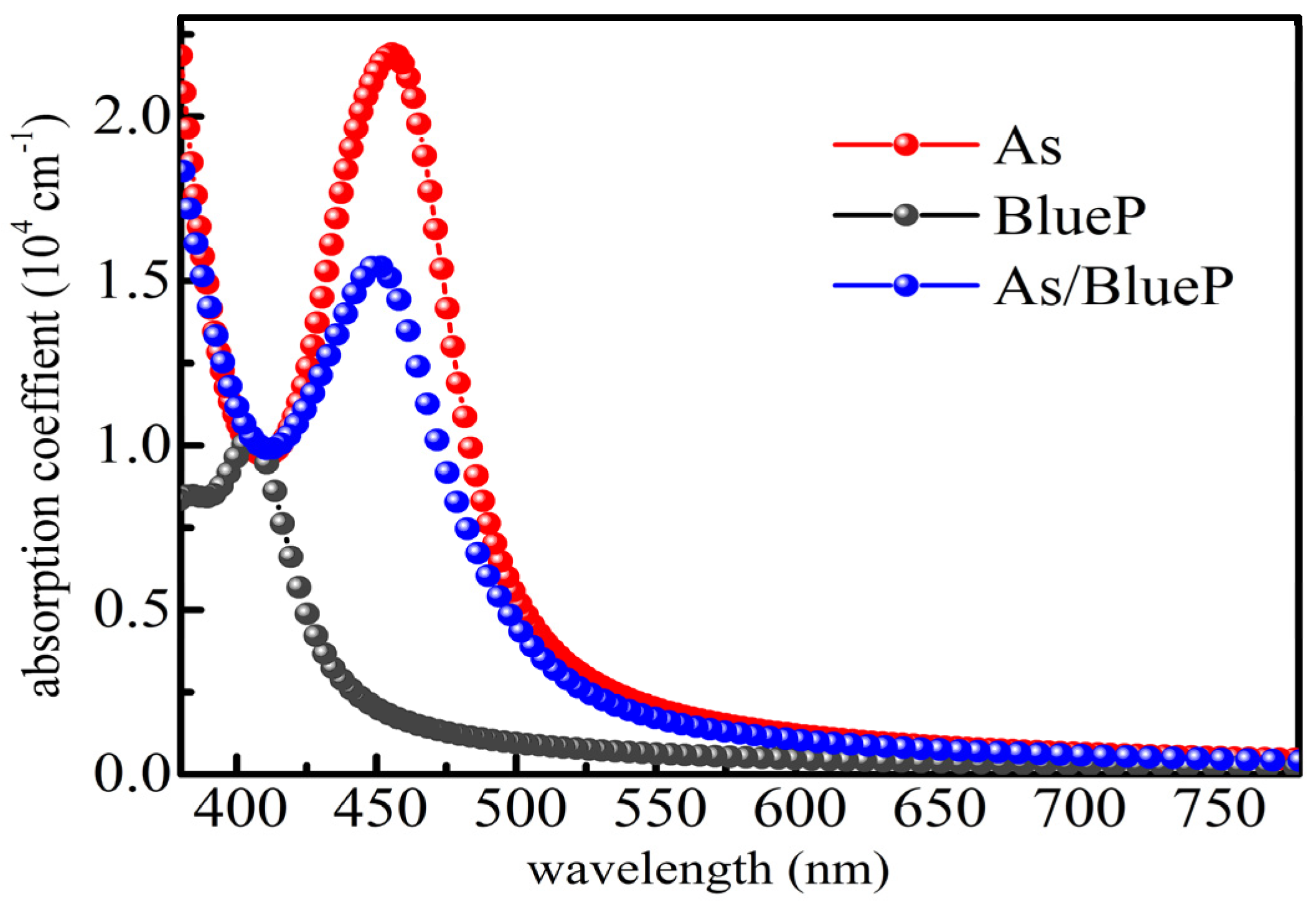
3.4. Optical Absorption Spectrum

A wide and strong optical absorption in visible light of the 2D material is crucial in generating electron-hole pairs, which is the first step for photocatalysis process of water splitting. Deduced from the frequency-dependent complex dielectric function ε(ω) = ε1(ω) + iε2(ω), the optical absorption coefficient can be calculated, as follows [51],
α ( ω ) = 2 ω [ ε 1 ( ω ) 2 + ε 2 ( ω ) 2 ε 1 ( ω ) ] 1 2
where ω is the frequency of incident light; ε1(ω) and ε2(ω) can be obtained using the Kramers–Kronig relation and summing all of the empty states in the Brillouin zone. Figure 4 shows the absorption spectrum of monolayer As, monolayer BlueP, and the As/BlueP hetero-structure.
The cut-off frequencies of the absorption spectrum are in good agreement with the band gaps shown in Figure 1 and Figure 3. Although the absorption coefficient of the As/BlueP hetero-structure is smaller than that of monolayer arsenene, it is much larger than that of monolayer BlueP. In addition, the optical absorption coefficient of the arsenene/BlueP hetero-structure is larger than the previously predicted the famous 2D g-C3N4 photocatalyst [52].

3.5. Photocatalytic Properties of the As/BlueP Hetero-Structure

For a high efficiency photocatalyst, its band edges are significantly important for redox reaction. For the water splitting reaction, the band edge alignment of the VBM and CBM must straddle the redox potentials of water. The oxidation potential and reduction potential of water splitting depends on the pH of the solution, as follows [53],
E O 2 / H 2 O o x = 5.67 + 0.059 × p H E O 2 / H 2 O r e d = 4.44 + 0.059 × p H
For a strong acid environment with pH = 0, the reduction potential level of hydrogen generation is −4.44 eV and the oxidation potential level of oxygen generation is −5.67 eV. Figure 5a illustrates the band edge alignment of the As/BlueP hetero-structure with respect to the vacuum level. The CBM of −4.03 eV is higher than the reduction potential, and the VBM of −5.86 eV is lower than the oxidation potential. When the As/BlueP hetero-structure is irradiated under sunlight, the electrons acquire enough energy to pass from the valence band to the conduction band. Additionally, then, the electron in the conduction band of the As layer can be easily stimulated in order to transfer to the conduction band of the BlueP layer due to the existence of the CBO. Nevertheless, the transmission of photo-generated holes in the BlueP layer to valence band of the As layer can be promoted by the VBO.
In addition to pH value of the solution, strain is expected to be another effective method for modulating the photocatalytic properties of the 2D semiconducting materials by adjusting its band edges and band alignment. Lots of previous researches have proved that the electronic properties of hetero-structure can be effectively improved by strain and further the photocatalytic properties, such as MoS2/WS2 [54], BlueP/Mg(OH)2 [31], and C2N/GaTe [55]. Therefore, we supply an in-layer biaxial strain to the As/BlueP hetero-structure, and the degree of deformation γ is defined as γ = (aa0)/a0, where a and a0 are the lattice constants of the structures with and without strains, respectively. Biaxial strain is applying the same γ in the periodic direction. Figure 5b shows the binding energies and band gap versus biaxial strain for the As/BlueP hetero-structure, where positive and negative γ mean tension and compression of the structure, respectively. When ε changes from −5% to 8%, the binding energy are always negative, indicating the stability of the As/BlueP vdW hetero-structure. Correspondingly, the band gap decreases with the increase of both tension and compression. It is noteworthy that the band gap keeps larger than 1.23 eV for the biaxial strain between −2.5% and 4.5%, which indicates the possibility of the hetero-structure to be a photocatalyst for water splitting.
Figure 5c displays the optical absorption as a function of biaxial tensile strain. With increase of biaxial strain from −4% to 4%, a red shift of optical absorption spectrum occurs, and more visible light with larger magnitude can be absorbed. That means a slight tension can effectively improve the optical absorption and further the catalytic efficiency of the hetero-structure. Finally, Figure 5d shows the band edge positions as a function of biaxial strain. For the unstrained As/BlueP hetero-structure with γ = 0, the larger energy gap between CBM and VBM makes an active water splitting reaction for a tolerant pH value from strong acid to neutral environments feasible. With an increase of tension or compression, the environment of the pH value changes the range to be narrower in order to make sure that both oxidation and reduction reactions to occur. When strain reaches −2.5% or 4.5%, the CBM and VBM just straddle the redox potentials, and only the solution with pH = 4 can participate in the photocatalysis of water splitting. Thus, by controlling the value of pH to match the redox potential of solution, the photocatalytic performance of water in different environments can be adjusted. Especially, when combined with the variation of optical absorption versus strain that is shown in Figure 5c, we infer that the highest photocatalytic efficiency can be achieved for the As/Blue hetero-structure at roughly 3.5% stretch deformation. It is worth mentioning that exerting stress on the hetero-structure has been proved to be an effective method for controlling the photocatalytic efficiency. The photocatalytic performance of the As/BlueP vdW hetero-structure under stress regulation is very similar to that of PC3 [16] and C2N/BlueP [46] hetero-structures proposed in previous theoretical researches.

4. Conclusions

In summary, we studied the structural, electronic, and optoelectronic properties of the designed 2D As/BlueP vdW hetero-structure by using the standard first principles calculation method. Especially, we found that the As/BlueP vdW hetero-structure can work as an efficient photocatalyst in water splitting. When an in-plane strain that is equal to 4.5% is applied to the hetero-structure, the optical absorption spectrum is effectively broadened in a visible light region, and the photocatalytic efficiency can be further improved. In view of the low carrier mobility and high light absorption in ultraviolet region, further research regarding the As/BlueP vdW hetero-structure will focus on how to improve the carrier mobility through external excitation, such as interlayer stress or electric field, and explore the possibility of its application as a ultraviolet photocatalyst. With excellent optical properties and the feature of type-II band alignment, we believe that the As/BlueP heterostructure can be a promising material in optoelectronic and photocatalytic devices.

Author Contributions

X.L., Y.L., L.L., T.X., and X.Z. performed the calculation part of the work and contributed to the tabulation, discussion of the results obtained, and revision of the final content to be submitted. B.W., B.J., Y.Y., and C.Y. carried out the planning and orientation of the calculation part and contributed to the critical review of the final work. All authors have read and agreed to the published version of the manuscript.

Funding

This study was supported by the National Nature Science Foundation of China (No. 61474039, No. 61774057, No. 11774238), the Open Fund of State Key Laboratory on Integrated Optoelectronics (IOSKL2018KF08), and Shenzhen Natural Science Foundations (Grant Nos. JCYJ20190808150409413 and JCYJ20190808115415679).

Conflicts of Interest

The authors declare no conflict of interest.

References

  1. Steven, C.; Arun, M. Opportunities and challenges for a sustainable energy future. Nature 2012, 488, 294–303. [Google Scholar]
  2. Seyed, E.H.; Mazlan, A.W. Hydrogen production from renewable and sustainable energy resources: Promising green energy carrier for clean development. Renew. Sustain. Energy Rev. 2016, 57, 850–866. [Google Scholar]
  3. Zhou, Y.N.; Zhu, Y.R.; Chen, X.Y.; Dong, B.; Li, Q.Z.; Chai, Y.M. Carbonebased transition metal sulfides/selenides nanostructures for electrocatalytic water splitting. J. Alloy. Compd. 2021, 852, 156810. [Google Scholar] [CrossRef]
  4. Philipp, A.; Hummel, P.; Schilling, T.; Feicht, P.; Rosenfeldt, S.; Ertl, M.; Schottle, M.; Lechner, A.M.; Xu, Z.; Gao, C.; et al. Anisotropic thermal transport in spray-coated single-phase two-dimensional materials: Synthetic clay versus graphene oxide. ACS Appl. Mater. Interfaces 2020, 12, 18785–18791. [Google Scholar] [CrossRef] [PubMed]
  5. Vovusha, H.; Amorim, R.G.; Scheicher, R.H.; Sanyal, B. Controlling the orientation of nucleobases by dipole moment interaction with graphene/h-BN interfaces. RSC Adv. 2018, 8, 6527. [Google Scholar] [CrossRef] [Green Version]
  6. Da, H.X.; Song, Q.; Dai, H.W.; Dong, P.; Bao, Q.L.; Ye, H.P.; An, Y.P.; Chen, J. Electrically controllable magneto-optic effects in a two-dimensional hexagonal organometallic lattice. Phys. Rev. B 2020, 101, 035423. [Google Scholar] [CrossRef]
  7. Wang, Q.; Li, J.W.; Yan, L.; Wang, B. KAgSe: A new two-dimensional efficient photovoltaic material with layer-independent behaviors. ACS Appl. Mater. Interfaces 2018, 10, 41670–41677. [Google Scholar] [CrossRef]
  8. Liu, Y.P.; Zeng, C.; Zhong, J.H.; Ding, J.N.; Wang, Z.M.M.; Liu, Z.W. Spintronics in two-dimensional materials. Nano-Micro Lett. 2020, 12, 1–26. [Google Scholar] [CrossRef] [Green Version]
  9. Choudhuri, I.; Bhauriyal, P.; Pathak, B. Recent advances in graphene-like 2D materials for spintronics applications. Chem. Mater. 2019, 31, 8260–8285. [Google Scholar] [CrossRef]
  10. Li, X.Y.; Lin, B.N.; Li, H.B.; Yu, Q.; Ge, Y.; Jin, X.; Liu, X.H. Carbon doped hexagonal BN as a highly efficient metal-free base catalyst for Knoevenagel condensation reaction. Appl. Catal. B 2018, 239, 254–259. [Google Scholar] [CrossRef]
  11. Liu, Y.; Deng, L.; Sheng, J.P.; Tang, F.Y.; Zeng, K.; Wang, L.Q.; Liang, K.X. Photostable core-shell CdS/ZIF-8 composite for enhanced photocatalytic reduction of CO2. Appl. Surf. Sci. 2019, 498, 143899. [Google Scholar] [CrossRef]
  12. Mohanty, B.; Chattopadhyay, A.; Nayak, J. Band gap engineering and enhancement of electrical conductivity in hydrothermally synthesized CeO2–PbS nanocomposites for solar cell applications. J. Alloy. Compd. 2021, 850, 156735. [Google Scholar] [CrossRef]
  13. Sainbileg, B.; Lai, Y.R.; Chen, L.C.; Hayashi, M. The dual-defective SnS2 monolayers: Promising 2D photocatalysts for overall water splitting. Phys. Chem. Chem. Phys. 2019, 21, 26292. [Google Scholar] [CrossRef] [PubMed]
  14. Wang, Q.; Li, J.W.; Liang, Y.; Wang, B.; Ning, Y.H. BX1–BX2 (X1, X2 = P, As, Sb) lateral heterostructure: Novel and efficient two-dimensional photovoltaic materials with ultra-high carrier mobilities. J. Mater. Chem. A 2019, 7, 10684. [Google Scholar] [CrossRef]
  15. Fang, Q.L.; Huang, Y.H.; Miao, Y.P.; Xu, K.W.; Li, Y.; Ma, F. Interfacial defect engineering on electronic states of two-dimensional AlN/MoS2 heterostructure. J. Phys. Chem. C 2017, 121, 6605–6613. [Google Scholar] [CrossRef]
  16. Yao, H.; Wang, Q.; Li, J.W.; Cai, W.S.; Wei, Y.D.; Wang, B.; Wang, J. Two-dimensional few-layered PC 3 as a promising photocatalyst for overall water splitting. Phys. Chem. Chem. Phys. 2020, 22, 9477–9486. [Google Scholar] [CrossRef]
  17. Obeid, M.M.; Bafekry, A.; Rehman, S.U.; Nguyen, C.V. A type-II GaSe/HfS2 van der Waals heterostructure as promising photocatalyst with high carrier mobility. Appl. Surf. Sci. 2020, 534, 147607. [Google Scholar] [CrossRef]
  18. Wang, G.Z.; Li, Z.F.; Wu, W.K.; Guo, H.; Chen, C.; Yuan, H.K.; Yang, S.Y.A. Two-dimensional h-BN/C2N heterostructure as a promising metal-free photocatalyst for overall water-splitting. Phys. Chem. Chem. Phys. 2020, 22, 24446–24454. [Google Scholar] [CrossRef]
  19. Azusa, M.; Mikiya, F.; Kenji, M.; Hiroki, M.; Hiroaki, B.; Hideo, O.; Shinzaburo, I.; Koichi, Y. Investigations on the charge transfer mechanism at donor/acceptor interfaces in the quest for descriptors of organic solar cell performance. Phys. Chem. Chem. Phys. 2018, 20, 12193. [Google Scholar]
  20. Zhang, J.L.; Zhao, S.T.; Han, C.; Wang, Z.Z.; Zhong, S.; Sun, S.; Guo, R.; Zhou, X.; Cheng, D.G.; Yuan, K.D.; et al. Epitaxial growth of single layer blue phosphorus: A new phase of two-dimensional phosphorus. Nano Lett. 2016, 16, 4903–4908. [Google Scholar] [CrossRef]
  21. Kaewmaraya, T.; Srepusharawoot, P.; Hussian, T.; Amornkitbamrung, V. Electronic Properties of h-BCN-Blue Phosphorene van der Waals Heterostructures. Chem. Phys. Chem. 2018, 19, 612–618. [Google Scholar] [CrossRef] [PubMed]
  22. Radisavljevic, B.; Radenovic, A.; Brivio, J.; Glacometti, V.; Kis, A. Single-layer MoS2 transistors. Nat. Nanotechnol. 2011, 6, 147–150. [Google Scholar] [CrossRef] [PubMed]
  23. Sun, M.L.; Tang, W.C.; Ren, Q.Q.; Wang, S.K.; Yu, J.; Du, Y.H. A first-principles study of light non-metallic atom substituted blue phosphorene. Appl. Surf. Sci. 2015, 356, 110–114. [Google Scholar] [CrossRef]
  24. Kamal, C.; Ezawa, M. Arsenene: Two-dimensional buckled and puckered honeycomb arsenic systems. Phys. Rev. B 2015, 91, 085423. [Google Scholar] [CrossRef] [Green Version]
  25. Fang, L.Z.; Li, X.P.; Geng, Z.D.; Wang, T.X.; Xia, C.X. Band alignment tuning in GeS/arsenene staggered hetero-structures. J. Alloy. Compd. 2019, 793, 283–288. [Google Scholar] [CrossRef]
  26. Jamdagni, P.; Thakur, A.; Kumar, A.; Ahluwalia, P.K.; Pandey, R. Two dimensional allotropes of arsenene with a wide range of high and anisotropic carrier mobility. Phys. Chem. Chem. Phys. 2018, 20, 29939. [Google Scholar] [CrossRef] [Green Version]
  27. Wang, C.; Xia, Q.L.; Nie, Y.Z.; Rahman, M. Strain engineering band gap, effective mass and anisotropic Dirac-like cone in monolayer arsenene. AIP Adv. 2016, 6, 035204. [Google Scholar] [CrossRef]
  28. Wang, Y.L.; Ding, Y. Electronic structure and carrier mobilities of arsenene and antimonene nanoribbons: A first-principle study. Nanoscale Res. Lett. 2015, 10, 254. [Google Scholar] [CrossRef] [Green Version]
  29. Zhang, S.L.; Yan, Z.; Li, Y.F.; Chen, Z.F.; Zeng, H.B. Atomically thin Arsenene and antimonene: Semimetal–semiconductor and indirect–direct band-gap transitions. Angew. Chem. Int. Ed. 2015, 127, 1–5. [Google Scholar]
  30. Huang, L.; Li, J.B. Tunable electronic structure of black phosphorus/blue phosphorus van der Waals p-n hetero-structure. Appl. Phys. Lett. 2016, 108, 083101. [Google Scholar] [CrossRef]
  31. Wang, B.J.; Li, X.H.; Cai, X.L.; Yu, W.Y.; Zhang, L.W.; Zhao, R.Q.; Ke, S.H. Blue Phosphorus/Mg(OH)2 van der Waals hetero-structures as Promising Visible-Light Photocatalysts for Water Splitting. J. Phys. Chem. C 2018, 122, 7075–7080. [Google Scholar] [CrossRef]
  32. Guo, J.J.; Zhou, G.P.; Li, H.H.; Wang, H.Y.; Liu, C. Tuning electronic properties of blue phosphorene/graphene-like GaN van der Waals hetero-structures by vertical external electric field. Nanoscale Res. Lett. 2019, 14, 174. [Google Scholar] [CrossRef] [PubMed]
  33. Ren, K.; Wang, S.; Luo, Y.; Xu, Y.J.; Sun, M.L.; Yu, J.; Tang, W.C. Strain-enhanced properties of van der Waals hetero-structure based on blue phosphorus and g-GaN as a visible-light-driven photocatalyst for water splitting. RSC Adv. 2019, 9, 4816. [Google Scholar] [CrossRef] [Green Version]
  34. Li, W.; Wang, T.X.; Dai, X.Q.; Ma, Y.Q.; Tang, Y.N. Effects of electric field on the electronic structures of MoS2/arsenene van der Waals heterostructure. J. Alloy. Compd. 2017, 705, 486–491. [Google Scholar] [CrossRef]
  35. Zeng, H.; Zhao, J.; Cheng, A.Q.; Zhang, L.; He, Z.; Chen, R.S. Tuning electronic and optical properties of arsenene/C3N van der Waals heterostructure by vertical strain and external electric field. Nanotechnology 2018, 29, 075201. [Google Scholar] [CrossRef]
  36. Li, Q.F.; Ma, X.F.; Lei, Z.; Wan, X.G.; Rao, W.F. Theoretical design of blue phosphorene/arsenene lateral heterostructures with superior electronic properties. J. Phys. D Appl. Phys. 2018, 51, 255304. [Google Scholar] [CrossRef]
  37. Kresse, G.; Furthmuller, J.; Hafner, J. Theory of the crystal structures of selenium and tellurium: The effect of generalized-gradient corrections to the local-density approximation. Phys. Rev. B 1994, 50, 17953. [Google Scholar] [CrossRef]
  38. Kresse, G.; Furthmuller, J. Efficient iterative schemes for Ab initio total-energy calculations using a plane-Wave Basis Set. Phys. Rev. B 1996, 54, 11169–11186. [Google Scholar] [CrossRef]
  39. Kresse, G.; Furthmüller, J. Efficiency of ab-initio total energy calculations for metals and semiconductors using a plane-wave basis set. Comput. Mater. Sci. 1996, 6, 15–50. [Google Scholar] [CrossRef]
  40. Heyd, J.; Scuseria, G.E. Hybrid functional based on a screened coulomb potential. J. Chem. Phys. 2003, 118, 8207. [Google Scholar] [CrossRef] [Green Version]
  41. Paier, J.; Marsman, M.; Hummer, K.; Kresse, G. Screened hybrid density functionals applied to solids. J. Chem. Phys. 2006, 124, 154709. [Google Scholar] [CrossRef] [Green Version]
  42. Grimme, S. Semiempirical GGA-type density functional constructed with a long-range dispersion correction. J. Comput. Chem. 2006, 27, 15. [Google Scholar] [CrossRef]
  43. Alfonso, D.R.; Ulloa, S.E. Molecular-dynamics simulations of methyl-radical deposition on diamond (100) surfaces. Phys. Rev. B 1993, 48, 16. [Google Scholar] [CrossRef] [PubMed]
  44. Wang, B.J.; Li, X.H.; Zhao, R.Q.; Cai, X.L.; Yu, W.Y.; Li, W.B.; Liu, Z.S.; Zhang, L.W.; Ke, S.H. Electronic structures and enhanced photocatalytic properties of blue phosphorene/BSe van der Waals heterostructures. J. Mater. Chem. A 2018, 6, 8923. [Google Scholar] [CrossRef]
  45. Xie, Z.F.; Sun, F.W.; Yao, R.; Zhang, Y.; Zhang, Y.H.; Zhang, Z.H.; Fan, J.B.; Ni, L.; Duan, L. Tuning electronic properties of InSe/arsenene heterostructure by external electric field and uniaxial strain. Appl. Surf. Sci. 2019, 475, 839–846. [Google Scholar] [CrossRef]
  46. Zhou, H.; Cai, W.S.; Li, J.W.; Liu, X.Y.; Xiong, W.; Zhou, Y.; Xu, Z.; Wang, B.; Ye, C. C2N/BlueP van der Waals hetero-structure: An efficient photocatalytic water splitting 2D material. Phys. Chem. Chem. Phys. 2020, 22, 1485–1492. [Google Scholar] [CrossRef]
  47. Li, X.H.; Wang, B.J.; Cai, X.L.; Zhang, L.W.; Wang, G.D.; Ke, S.H. Tunable electronic properties of arsenene/GaS van der Waals heterostructures. RSC Adv. 2017, 7, 28393. [Google Scholar] [CrossRef] [Green Version]
  48. Sun, M.L.; Chou, J.P.; Gao, J.F.; Cheng, Y.; Hu, A.; Tang, W.C.; Zhang, G. Exceptional optical Absorption of buckled arsenene covering a broad spectral range by molecular doping. ACS Omega 2018, 3, 8514–8520. [Google Scholar] [CrossRef] [Green Version]
  49. Liu, N.S.; Zhou, S. Gas adsorption on monolayer blue phosphorus: Implications for environmental stability and gas sensors. Nanotechnology 2017, 28, 175708. [Google Scholar] [CrossRef] [Green Version]
  50. Li, G.; Zhao, Y.C.; Zeng, S.M.; Ni, J. The realization of half-metal and spin-semiconductor for metal adatoms on arsenene. Appl. Surf. Sci. 2016, 390, 60–67. [Google Scholar] [CrossRef]
  51. Kuzmenko, A.B. Kramers–Kronig constrained variational analysis of optical spectra. Rev. Sci. Instrum. 2005, 76, 083108. [Google Scholar] [CrossRef] [Green Version]
  52. Ma, X.G.; Lv, Y.H.; Xu, J.; Liu, Y.F.; Zhang, R.Q.; Zhu, Y.F. A strategy of enhancing the photoactivity of g-C3N4 via doping of nonmetal elements: A first-principles study. J. Phys. Chem. C 2012, 116, 23485–23493. [Google Scholar] [CrossRef]
  53. Singh, A.K.; Mathew, K.; Zhuang, H.L.; Henning, R.G. Computational screening of 2D materials for photocatalysis. J. Phys. Chem. Lett. 2015, 6, 1087–1098. [Google Scholar] [CrossRef] [PubMed]
  54. Farkous, M.; Bikerouin, M.; Thuan, D.V.; Benhouria, Y.; El-Yadri, M.; Feddi, E.; Erguig, H.; Dujardin, F.; Nguyen, C.V.; Hieu, N.V.; et al. Strain effects on the electronic and optical properties of Van der Waals hetero-structure MoS2/WS2: A first-principles study. Phys. E 2020, 116, 113799. [Google Scholar] [CrossRef]
  55. Bai, Y.J.; Zhang, Q.F.; Xu, N.; Deng, K.M.; Kan, E. Efficient carrier separation and band structure tuning of two-dimensional C2N/GaTe van der Waals hetero-structure. J. Phys. Chem. C 2018, 122, 15892–15902. [Google Scholar] [CrossRef]
Figure 1. Schematic views of (a) As and (b) BlueP monolayers from top view and side view. The green and purple spheres represent As and P atoms, respectively. The dash curve rhombuses in (a) and (b) show a supercell and a 3 × 3 supercell, respectively. (c,d) The band structures of (c) As and (d) BlueP monolayers calculated based on HSE06 exchange-correlation functional. (e,f) Total and partial DOS of (e) As and (f) BlueP monolayers based on HSE06 exchange-correlation functional.
Coatings 10 01160 g001
Figure 2. (a) Top and side views of the optimized As/BlueP vdW hetero-structure. (b) Total energy evolution of the hetero-structure at 300 K from AIMD simulations. Insets depict the snapshot of the hetero-structure at 10 ps from top and side views.
Coatings 10 01160 g002
Figure 3. (a) Projected band structure and DOS of the As/BlueP hetero-structure based on HSE06 exchange-correlation functional. (b) Isosurface plot of real space charge distribution at CBM and VBM of the hetero-structure with isovalue equal to 0.002 e/Bohr3. (c) Band edges and band alignment of monolayer As, monolayer BlueP and the As/BlueP hetero-structure. (d) The electrostatic potential and plane-averaged differential charge density of the As/BlueP hetero-structure along z-direction.
Coatings 10 01160 g003
Figure 4. Optical absorption coefficient in the visible light region of monolayer As, monolayer BlueP, and the As/BlueP hetero-structure.
Coatings 10 01160 g004
Figure 5. (a) Schematic illustration of the type-II photocatalytic mechanism of As/BlueP hetero-structure. The horizontal dash lines indicate the oxidation potential and reduction potential for water splitting. (b) Bandgap and binding energy of the As/BlueP hetero-structure as functions of the tunable biaxial strain based on the HSE06 calculation. (c) Optical absorption coefficient of As/BlueP hetero-structures with different biaxial strain versus incident light energy. (d) Band edge positions of As/BlueP hetero-structure as functions of the tunable interlayer distance. The horizontal dash lines indicate the oxidation potential and reduction potential for water splitting at different pH.
Coatings 10 01160 g005
Publisher’s Note: MDPI stays neutral with regard to jurisdictional claims in published maps and institutional affiliations.

