SnSe2 Quantum Dots: Facile Fabrication and Application in Highly Responsive UV-Detectors

 ,
, 
Abstract
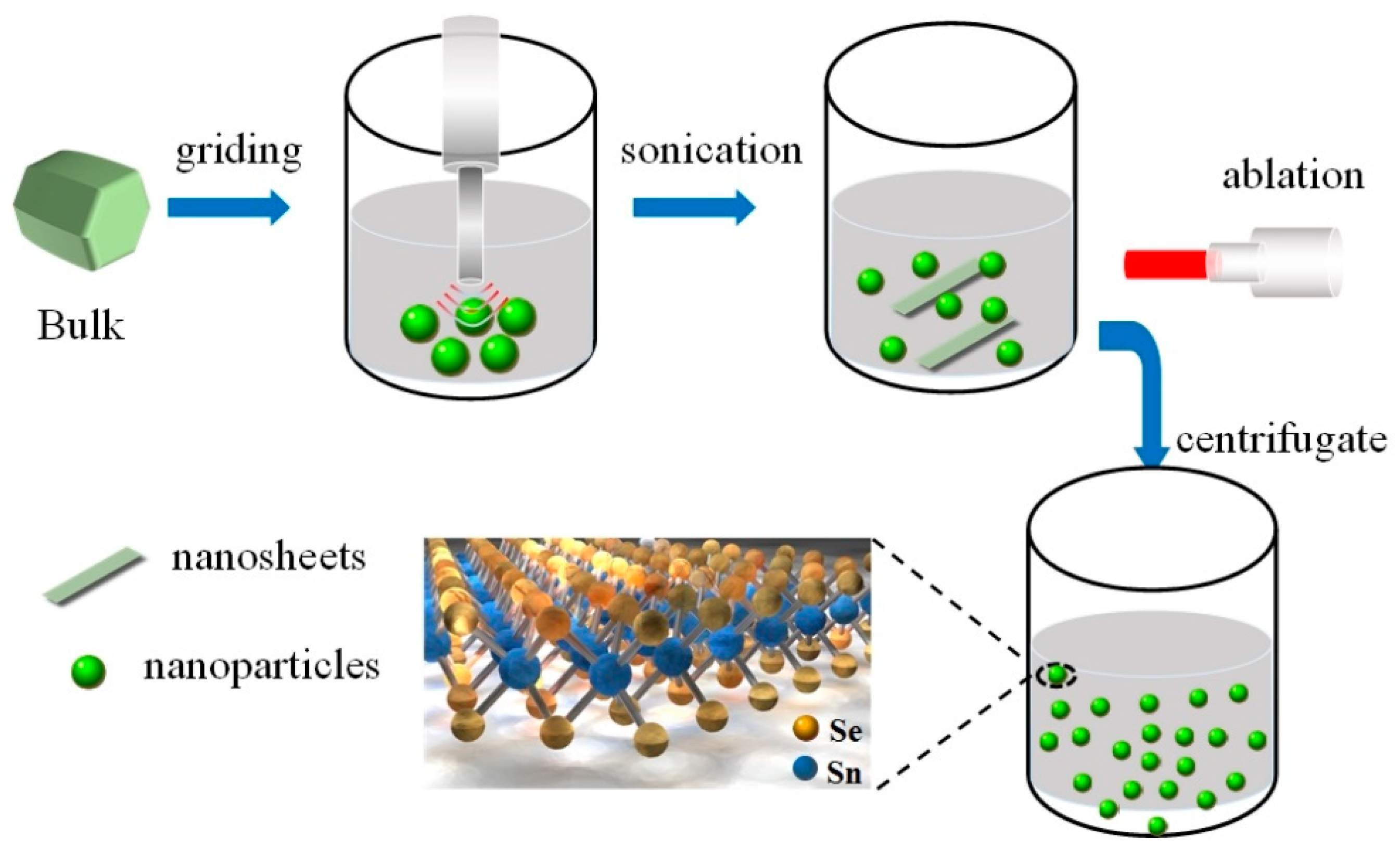
:1. Introduction
2. Experiment
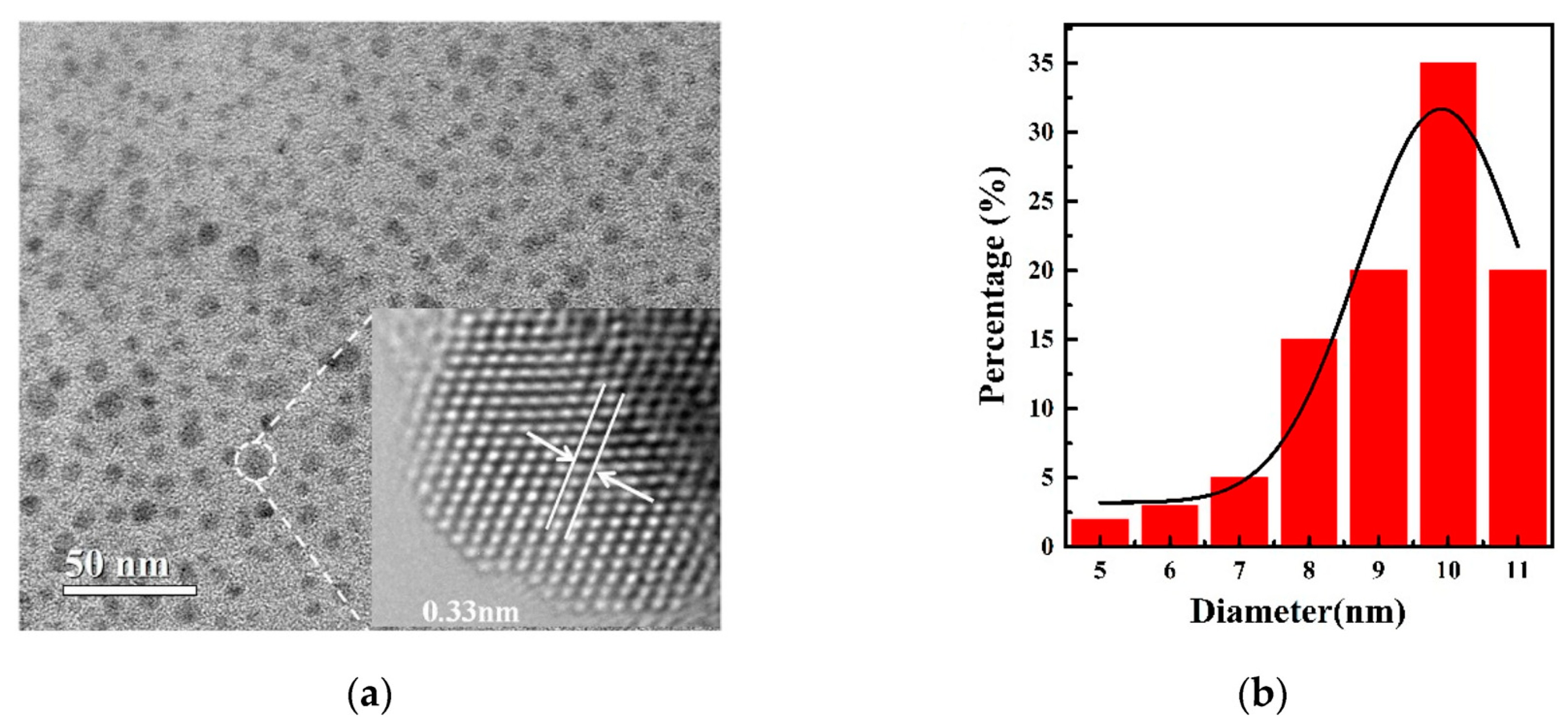
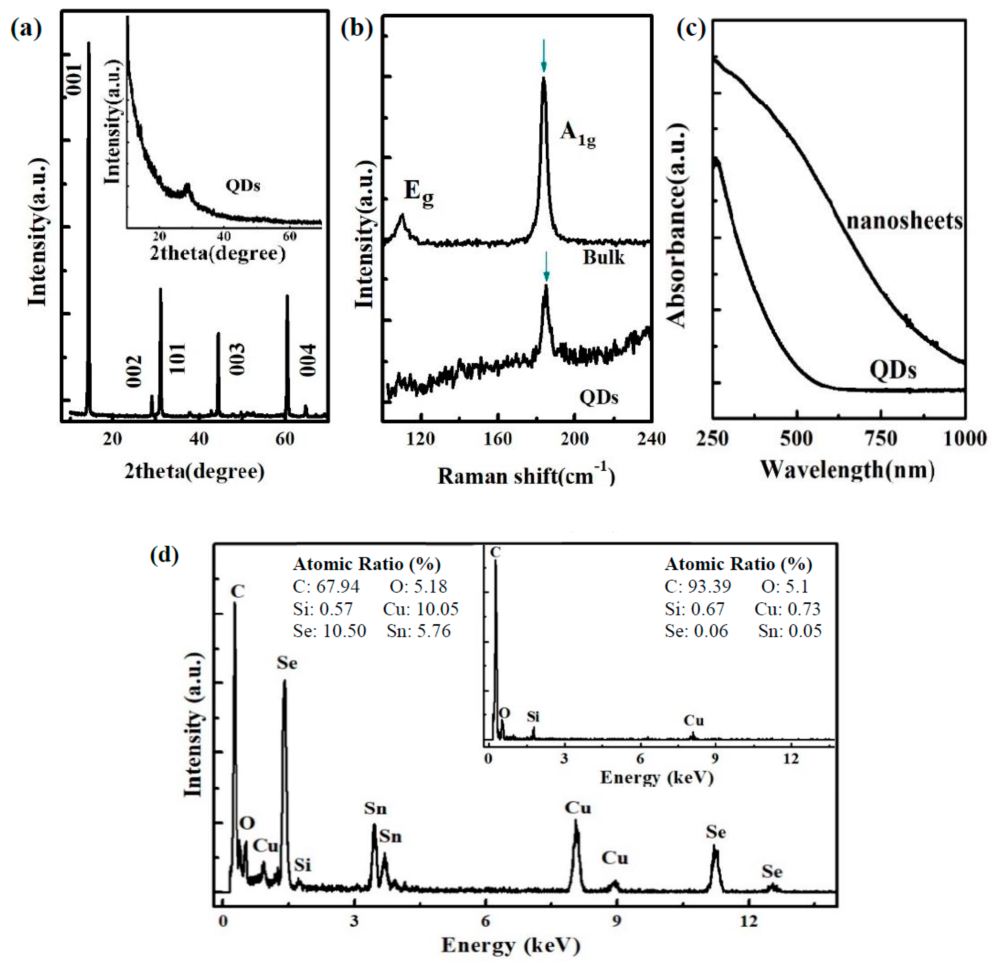
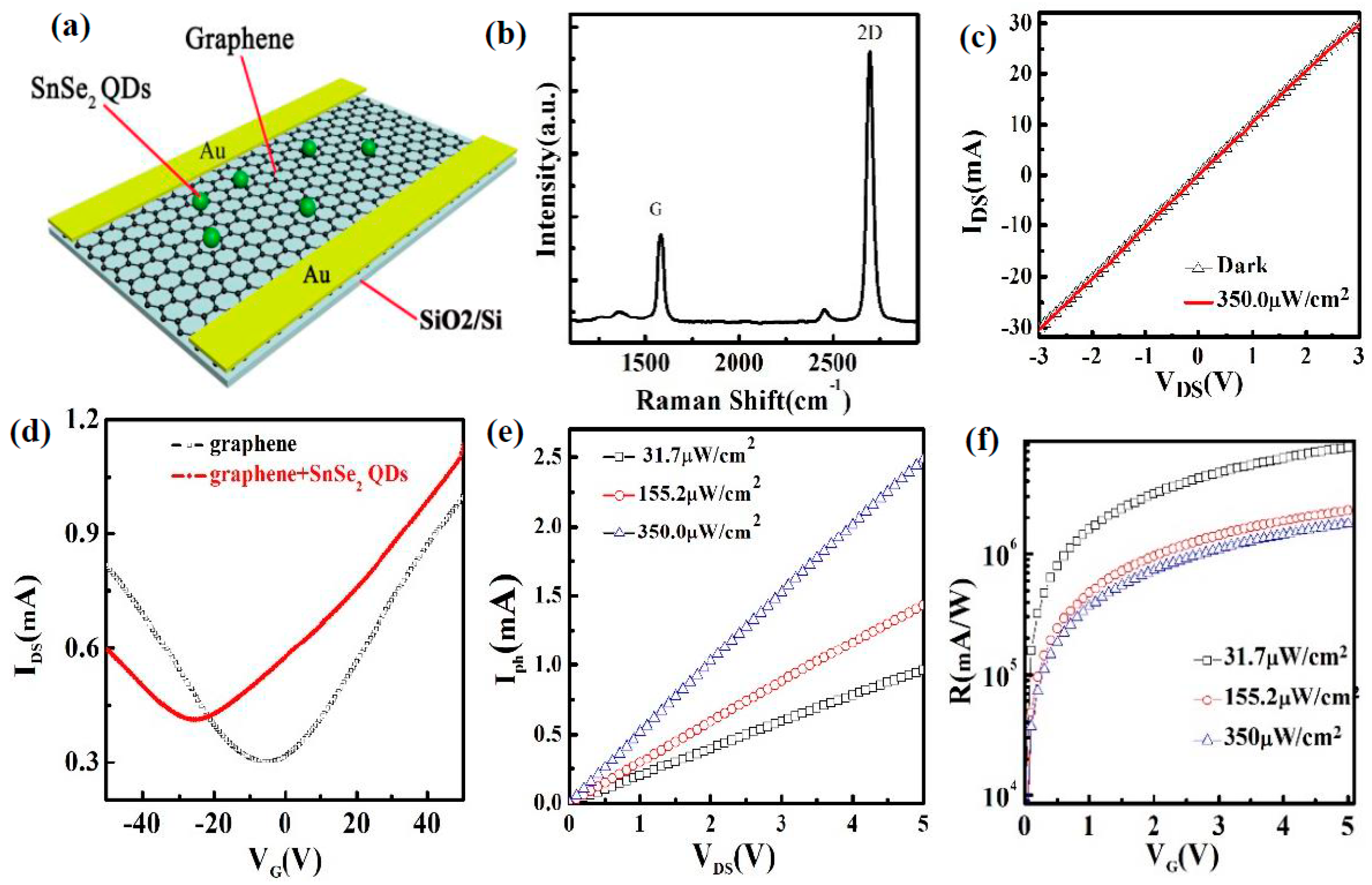
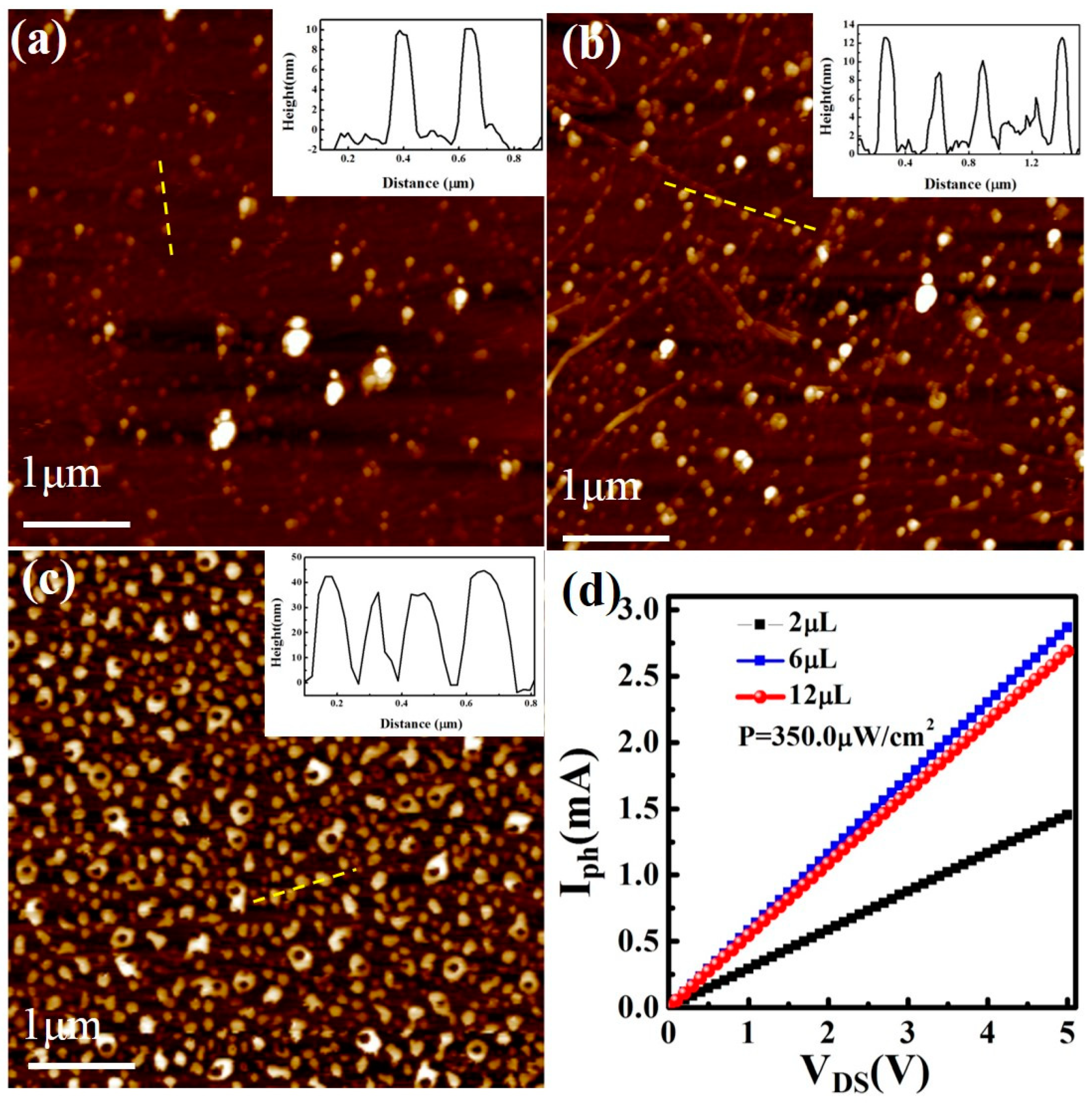
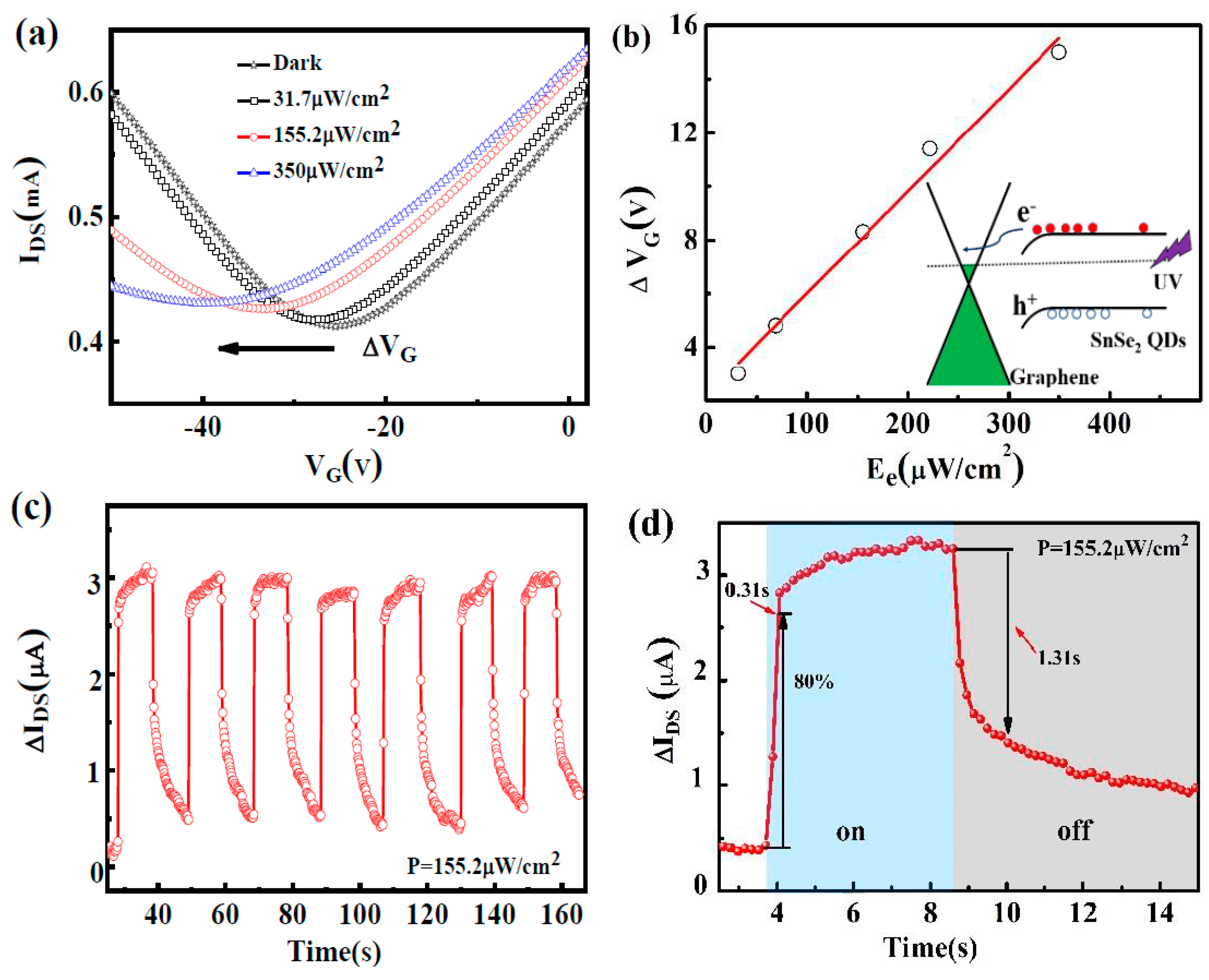
3. Results and Discussion
4. Conclusions
Author Contributions
Funding
Acknowledgments
Conflicts of Interest
References
- Bonaccorso, F.; Sun, Z.; Hasan, T.; Ferrari, A.C. Graphene Photonics and Optoelectronics. Nat. Photonics 2010, 4, 611–622. [Google Scholar] [CrossRef]
- Xia, F.; Thomas, M.; Lin, Y.; Valdes, Y.; Phaedon, A. Ultrafast Graphene Phototransistor. Nat. Nanotechnol. 2009, 4, 839–843. [Google Scholar] [CrossRef] [PubMed]
- Li, X.; Li, T.; Chen, Z.; Fang, H.; Li, X.; Wang, X.; Xu, J.; Zhu, H. Graphene and Related Two-Dimensional Materials: Structure-Property Relationships for Electronics and Optoelectronics. Appl. Phys. Rev. 2017, 4, 021306. [Google Scholar] [CrossRef]
- Mueller, T.; Xia, F.; Phaedon, A. Graphene Phototransistors for High-Speed Optical Communications. Nat. Photonics 2010, 4, 297–301. [Google Scholar] [CrossRef]
- Li, X.M.; Zhu, H. The Graphene–Semiconductor Schottky Junction. Phys. Today 2016, 69, 46–51. [Google Scholar] [CrossRef]
- Liu, C.; Chang, Y.; Theodore, B.; Zhong, Z. Graphene Phototransistors with Ultra-Broadband and High Responsivity at Room Temperature. Nat. Nanotechnol. 2014, 9, 273–278. [Google Scholar] [CrossRef] [PubMed]
- Fitzmorris, B.; Pu, Y.; Jason, K.; Lin, Y.; Hu, Y.; Li, U.; Zhang, J. Optical Properties and Exciton Dynamics of Alloyed Core/Shell/Shell Cd1-XZnxSe/ZnSe/ZnS Quantum Dots. ACS Appl. Mater. Interfaces 2013, 5, 2893–2900. [Google Scholar] [CrossRef]
- Cheng, S.; Weng, T.; Lu, M.; Tan, W.; Chen, J.; Chen, Y. All Carbon-Based Phototransistors: An Eminent Integration of Graphite Quantum Dots and Two Dimensional Graphene. Sci. Rep. 2013, 3, 2694. [Google Scholar] [CrossRef]
- Sun, Z.; Liu, Z.; Li, J.; Tai, G.; Lan, S.; Yan, F. Infrared Phototransistors Based on CVD-Grown Graphene and PbS Quantum Dots with Ultrahigh Responsivity. Adv. Mater. 2012, 24, 5878–5883. [Google Scholar] [CrossRef]
- Sun, Y.; Dan, X.; Sun, M.; Teng, C.; Liu, Q.; Chen, R.; Lan, X.; Ren, T. Hybrid Graphene/Cadmium-Free ZnSe/ZnS Quantum Dots Phototransistors for UV Detection. Sci. Rep. 2018, 8, 1–8. [Google Scholar] [CrossRef]
- Long, H.; Li, T.; Chun, P.; Chun, Y.; Kin, H.; Yang, C.; Tsang, Y. The WS2 Quantum Dot: Preparation, Characterization and Its Optical Limiting Effect in Polymethylmethacrylate. Nanotechnology 2016, 27, 414005. [Google Scholar] [CrossRef] [PubMed]
- Han, Y.; Zhang, C.; Gu, W.; Ding, C.; Li, X.; Xian, Y. Facile Synthesis of Water-Soluble WS2 Quantum Dots for Turn-on Fluorescent Measurement of Lipoic Acid. J. Phys. Chem. C 2016, 120, 12170–12177. [Google Scholar]
- Xu, S.; Li, D.; Wu, P. One-Pot, Facile, and Versatile Synthesis of Monolayer MoS2/WS2 Quantum Dots as Bioimaging Probes and Efficient Electrocatalysts for Hydrogen Evolution Reaction. Adv. Funct. Mater. 2015, 7, 1127–1136. [Google Scholar] [CrossRef]
- He, R.; Peng, L.; Liu, Z.; Zhu, H.; Zhao, X.; Chan, H.; Yan, F. Solution-Gated Graphene Field Effect Transistors Integrated in Microfluidic Systems and Used for Flow Velocity Detection. Nano Lett. 2012, 12, 1404–1409. [Google Scholar] [CrossRef] [PubMed]
- Chiang, C.W.; Haider, G.; Tan, W.C.; Chen, Y.F. Highly Stretchable and Sensitive Photodetectors Based on Hybrid Graphene and Graphene Quantum Dots. ACS Appl. Mater. Interfaces. 2016, 8, 466–471. [Google Scholar] [CrossRef] [PubMed]
- Zhou, X.; Lin, G.; Tian, W.; Zhang, Q.; Jin, S.; Li, H.; Yoshio, B.; Dmitri, G.; Zhai, T. Ultrathin SnSe2 Flakes Grown by Chemical Vapor Deposition for High-Performance Phototransistors. Adv. Mater. 2015, 27, 8035–8041. [Google Scholar] [CrossRef]
- Zankat, C.; Pratik, P.; Solanki, G.K.; Patel, K.V.; Pathak, M.; Som, N.; Prafulla, J. Investigation of Morphological and Structural Properties of V Incorporated SnSe2 Single Crystals. Mater. Sci. Semicond. Process. 2018, 8, 137–142. [Google Scholar] [CrossRef]
- Zhou, W.; Yu, Z.; Song, H.; Fang, R.; Wu, Z.; Li, L.; Ni, Z.; Wei, R.; Lin, W.; Ruan, S. Lattice Dynamics in Monolayer and Few-Layer SnSe2. Physcal Rev. B 2017, 96, 035401. [Google Scholar] [CrossRef]
- Qiao, X.; Wu, J.; Zhou, L.; Qiao, J.; Shi, W.; Chen, T.; Zhang, X.; Zhang, J.; Ji, W.; Tan, P.H. Polytypism and Unexpected Strong Interlayer Coupling of Two-Dimensional Layered ReS2. Adv. Funct. Mater. 2015, 8, 8324–8332. [Google Scholar] [CrossRef]
- Borges, Z.V.; Poffo, C.M.; de Lima, J.C.; de souza, S.M.; Trichês, D.M.; Nogueira, T.P.O.; Manzato, L.; de Biasi, R.S. Study of Structural, Optical and Thermal Properties of Nanostructured SnSe2 Prepared by Mechanical Alloying. Mater. Chem. Phys. 2016, 169, 47–54. [Google Scholar] [CrossRef]
- Solati, E.; Laya, D.; Davoud, D. Effect of Laser Pulse Energy and Wavelength on the Structure, Morphology and Optical Properties of ZnO Nanoparticles. Opt. Laser Technol. 2014, 58, 26–32. [Google Scholar] [CrossRef]
- Kathalingam, A.; Senthilkumar, V.; Rhee, J.-K. Hysteresis I-V nature of mechanically exfoliated graphene FET. J. Mater. Sci. Mater. Electron. 2014, 25, 1303–1308. [Google Scholar] [CrossRef]
- Cheng, W.; Tang, L.; Xiang, J.; Ji, R.; Zhao, J. An Extreme High-Performance Ultraviolet Photovoltaic Detector Based on Zno Nanorods/Phenanthrene Heterojunction. RSC Adv. 2016, 6, 12076–12080. [Google Scholar] [CrossRef]
- Babichev, A.V.; Zhang, H.; Pierre, L.; Julien, F.H.; Egorov, Y.; Lin, Y.; Tu, L.; Maria, T. Gan Nanowire Ultraviolet Phototransistor with a Graphene Transparent Contact. Appl. Phys. Lett. 2013, 103, 201103. [Google Scholar] [CrossRef]
- Boruah, B.; Anwesha, M.; Abha, M. Sandwiched Assembly of Zno Nanowires between Graphene Layers for a Self-Powered and Fast Responsive Ultraviolet Phototransistor. Nanotechnology 2016, 27, 095205. [Google Scholar] [CrossRef] [PubMed]
- Lu, Y.; Wu, Z.; Xu, W.; Lin, S. ZnO Quantum Dot-Doped Graphene/H-BN/Gan-Heterostructure Ultraviolet Phototransistor with Extremely High Responsivity. Nanotechnology 2016, 26, 48LT03. [Google Scholar] [CrossRef] [PubMed]
- Tang, J.; Kyle, K.; Sjoerd, H.; Kwang, J.; Liu, H.; Larissa, L.; Melissa, F.; Wang, X.; Ratan, D.; Dongkyu, C.; et al. Colloidal-Quantum-Dot Photovoltaics Using Atomic-Ligand Passivation. Nat. Mater. 2011, 10, 765–771. [Google Scholar] [CrossRef] [PubMed]


© 2019 by the authors. Licensee MDPI, Basel, Switzerland. This article is an open access article distributed under the terms and conditions of the Creative Commons Attribution (CC BY) license (http://creativecommons.org/licenses/by/4.0/).
Share and Cite
Li, X.; Li, L.; Zhao, H.; Ruan, S.; Zhang, W.; Yan, P.; Sun, Z.; Liang, H.; Tao, K. SnSe2 Quantum Dots: Facile Fabrication and Application in Highly Responsive UV-Detectors. Nanomaterials 2019, 9, 1324. https://doi.org/10.3390/nano9091324
Li X, Li L, Zhao H, Ruan S, Zhang W, Yan P, Sun Z, Liang H, Tao K. SnSe2 Quantum Dots: Facile Fabrication and Application in Highly Responsive UV-Detectors. Nanomaterials. 2019; 9(9):1324. https://doi.org/10.3390/nano9091324
Chicago/Turabian StyleLi, Xiangyang, Ling Li, Huancheng Zhao, Shuangchen Ruan, Wenfei Zhang, Peiguang Yan, Zhenhua Sun, Huawei Liang, and Keyu Tao. 2019. "SnSe2 Quantum Dots: Facile Fabrication and Application in Highly Responsive UV-Detectors" Nanomaterials 9, no. 9: 1324. https://doi.org/10.3390/nano9091324
APA StyleLi, X., Li, L., Zhao, H., Ruan, S., Zhang, W., Yan, P., Sun, Z., Liang, H., & Tao, K. (2019). SnSe2 Quantum Dots: Facile Fabrication and Application in Highly Responsive UV-Detectors. Nanomaterials, 9(9), 1324. https://doi.org/10.3390/nano9091324