3.1. Nanocomposites PVK-Colloidal CdS NCs
Our first goal was to incorporate the synthesized CdS NCs as part of the active layer in hybrid LEDs based in PVK polymer. To this purpose we prepared the active layer nanocomposite mixing the solution of colloidal CdS NCs in DMSO with a solution of PVK in toluene. The solution for LEDs active layers had a PVK:CdS mass ratio of 1:1 with a concentration of 3% by weight of the hybrid solution. In addition, a reference of PVK in toluene, without nanoparticles, was also prepared at 3 wt%. Optical absorption and PL measurements were carried out in these solutions.
Figure 1 shows the absorption curves corresponding to pristine PVK and hybrid PVK:CdS(col) solutions. We observed that the solution with nanoparticles exhibit an evident increase in absorbance with respect to the PVK sample for wavelengths above 370 nm. The background absorption at visible wavelengths increases for the hybrid solution in the whole range. The absorption edge due to the presence of CdS NCs can be seen as a shoulder appearing around 400 nm. The inset in
Figure 1 shows absorbance and PL spectra of a solution of colloidal CdS NCs in DMSO. A value of 3.253 eV (381.17 nm) was obtained for the absorption band edge. The maximum for light emission, with an excitation wavelength of 365 nm, is found at 480 nm.
For CdS NCs synthesized at low temperatures, it is common to observe broad photoluminescence emission bands attributed to trap emission from deep surface states primarily resulting from defects in the nanocrystals surface. The most frequent defects in CdS NCs are sulphur or cadmium vacancies, interstitial sulphur and cadmium atoms adsorbed on the NP surface [
30]. The big distance between emission wavelength and absorption onset, close to 100 nm in the inset of
Figure 1, is indicative of such emission from deep surface states in the NCs.
The size of the CdS nanoparticles can be estimated by the equation suggested by Brus [
31]:
where
En is the energy gap of CdS nanoparticles, and
Eb = 2.42 eV is the energy gap of bulk material, ε = 5.7 is the dielectric constant,
me* = 0.19
m0 is effective mass of electron, and
mh* = 0.80
m0 is effective mass of hole (
m0 is the rest mass of electron).
The estimated diameter of these colloidal CdS NCs is shown in
Table 1.
The normalized PL spectra of the pristine PVK and hybrid solutions are plotted in
Figure 2. The excitation wavelength is λ
exc = 365 nm. The hybrid curve (red) presents a main peak related to PVK emission and the influence of the CdS NCs can be perceived as a shoulder at longer wavelengths. The solution without CdS shows the PVK characteristic emission peak at 400 nm corresponding to the excimer emission of PVK [
13]. In the solution with nanoparticles, the PL is defined by a strong emission peak at approximately 415 nm related to the polymer emission. The red-shift in emission wavelength might be due to well-known dependence on solvent polarizability. DMSO is a highly polar solvent, so the distance between polymer molecules decreases, therefore increasing local polarization field and producing the shift observed with PVK emission [
32].
The asymmetry of the peak on the longer wavelength side is generated by the influence of the CdS nanoparticles. The emission intensity coming from the NCs is low and it is expected at wavelengths very close to the emission from the PVK, thus its effect is hidden for this ratio of NCs.
3.2. Hybrid LED with CdS Colloidal Nanoparticles
Hybrid light-emitting diodes with the configuration shown in
Figure 3 were fabricated following the procedure described in
Section 2.3. The previously characterized solutions were used as the starting material for the emissive layers. CdS NCs in DMSO were mixed with PVK dissolved in toluene with 1:1 mass ratio. The concentration of this solution was at 3 wt%.
Two types of LEDs were manufactured. The first one is the reference, organic LED with pristine PVK emissive layer. In the other one, the active layer consists of the mixture of PVK and CdS(col) NCs.
We measured the current density vs. voltage (J–V) curves of these LEDs. The results are shown in
Figure 4A. Hybrid LEDs using CdS NCs in DMSO solution presented a resistive behaviour and they did not show any electroluminescence. Except for the pristine PVK LED, all the hybrid devices we fabricated using colloidal CdS NCs did not exhibit a uniform surface.
Given the results of the J–V curves and the absence of light emission for these devices, characterization by atomic force microscope (AFM) was performed to observe in detail the surface of the hybrid devices (see
Figure 4B).
In the spin-coating technique, the solvent is removed from the film due to the speed of rotation as well as the time used in the process. However, the density and viscosity of solvents are factors to take into account. In order to not modify the conditions of the manufacturing route, the rotation speed, and the time of spinning were exactly the same for all the fabricated devices.
In the spinning process, the solvents undergo the gravity and the centrifugal force, and a viscous force caused by the solvent viscosity. This viscous force is a friction force, contrary to the centrifugal force. The density of the solvent increases the gravity and centrifugal force and the viscosity increases the viscous force. The density/viscosity ratio conditions the spin-coating process. For toluene, this ratio is 1.47 whilst for DMSO it is only 0.55. In films where both solvents are present, the difference in these ratios produces artifacts in the active layer. The solvent with the highest density/viscosity ratio tends to remain in the lower part of the layer and/or it is quickly spelt out of the substrate. DMSO could prevent a proper elimination of toluene because its density/viscosity ratio is lower and disturbs toluene mobility, causing solvent areas of toluene that are not eliminated, remaining in the film under DMSO. On the other hand, DMSO with a lower density/viscosity ratio is prone to remain in the upper part of the liquid film and last longer over the film surface prior to be expelled from the substrate. Solvent areas could be eliminated by increasing the spin speed or time in the process, but increasing these parameters, the nanoparticles are probably blown away.
With subsequent heating, the solvent residues evaporate. The toluene areas are evaporated and very small bubbles remain in the active layer. When the toluene evaporates, the tiny craters (black spots) that we observe in
Figure 4B are created. A statistical study has been performed and the craters have an average depth of 12.5 ± 0.6 nm. During the evaporation of the cathode, aluminium is introduced into the craters, causing narrowing between anode and cathode and micro short circuits. This situation can create the resistive behaviour that we have observed in the J–V curves, see
Figure 4A, because electrons flow may have a preference for narrowing and not for the thicker active layer. This can also be a reason why these devices do not show electroluminescence.
Furthermore, in
Figure 4B, some isolated circular monticules, bright white spots of hundreds of nanometres diameter, are observed. These white protuberances, close to 100 nm height, can be agglomerations of nanoparticles because the nanoparticles surrounded with thiophenol ligands are soluble only in DMSO and they tend to remain in this solvent. If microscopic drops of DMSO hold on the surface of the sample after the spinning process, the solvent will evaporate by post-annealing and the NCs in DMSO will agglomerate forming these peaks on the top of the layer.
The confluence of high peaks of, presumably, CdS NCs, and tiny craters in the PVK matrix within a short distance, is probably the cause to these hybrid LEDs malfunction.
3.3. Preparation of Evaporated CdS Nanoparticles Powder
The inadequate morphology of the active layer, found in the devices manufactured in the previous section, is possibly due to the presence of two solvents with quite different properties. To eliminate the DMSO present in the active layer solution, we have tested a very simple method to obtain nanoparticles to embed in the PVK matrix. Instead of performing a complex, time consuming and more expensive ligand-exchange process to remove thiols from the NCs surface and replace them with other ligand soluble in toluene, we decided to simply evaporate the DMSO from colloidal CdS NCs solutions by heating.
Thermal gravimetric analysis (TGA) and differential scanning calorimetry (DSC) were performed to check the cadmium thiolate stability with the temperature. The results are displayed in
Figure 5. To eliminate the solvent, a temperature of 200 °C was chosen, because this temperature does not produce changes of mass or state in Cd(C
6H
5S)
2 (
Figure 5) and is higher than DMSO boiling point (189 °C). For this experiment we used solutions of CdS NCs synthesized in DMSO, like the one studied in
Section 2.2. CdS(col). One day after the synthesis process, the solution was heated at 200 °C on a heating plate. Once the solvent was evaporated, a yellow powder of CdS NCs is gathered in the bottom of the vessel. Dry evaporated CdS nanocrystals with their capping are obtained CdS(eva).
Powder of CdS (eva) NCs was redispersed in toluene and optical absorption and photoluminescence measurements were carried out and compared to CdS(col) measurements. According to Youssef et al. [
33], the thermogravimetry of CdS nanoparticles shows that significant changes due to temperature occur at temperatures quite higher than 200 °C, mostly around 275 °C. Below that temperature it should be expected that heating does not modify the structure of the nanoparticles.
Nevertheless, in our experiment, the heating received during the evaporation causes the photoluminescence to be activated increasing photoluminescence intensity. In addition, a red shift of the maximum position of the CdS emission peak is observed.
Figure 6 shows the comparison between normalized PL emission of colloidal CdS NCs as synthesized in DMSO (black squares) and these dried CdS(eva) NCs redispersed in toluene (blue squares). The CdS emission peak shift is clearly seen. The colloidal CdS nanoparticles synthesized directly in DMSO have their maximum emission at 480 nm while for evaporated CdS NCs redispersed in toluene, the maximum is located at 586 nm. Moreover, a PL emission enhancement is clearly observed. This increased PL efficiency after heating has been previously reported in CdS NCs [
34] and attributed to reduced local strain and nonradiative decay centres after annealing. Optical absorption was also registered for these evaporated NCs dispersed in toluene, and compared, in
Figure 7, with the absorption of the NCs prior to evaporation.
Figure 7 corroborates that evaporation produces also a shift of absorption edge towards a longer wavelength and a lower energy gap. Comparative values of absorption edge for both types of NCs are collected in
Table 1. The increase of absorbance observed for evaporated NCs, especially at longer wavelengths, is due to the fact that these NCs are dispersed in toluene, where they are not soluble, producing high scattering.
An estimation of the evaporated CdS NCs size is done using Brus Equation (1), and the results also included in
Table 1. According to this, the evaporation of the DMSO solvent goes along with the increase in size of the NCs.
In order to check the different size of NCs before and after the evaporative heating, transmission electron microscopy (TEM) analysis has been performed. To perform TEM analysis, a drop of the NCs solution was deposited on a carbon grid and then dried at room temperature.
For the as synthesized CdS(col) NCs in DMSO a TEM study with more than 90 nanoparticles was conducted. An average size is calculated for these nanoparticles of 3.07 ± 0.07 nm (sample in
Figure 8A). In
Figure 8B, the same study was performed for the DMSO-free cadmium sulfide NCs CdS(eva). In this case, the obtained average size is 4.12 ± 0.12 nm. A wider size distribution is found in the samples with evaporated nanocrystals.
Figure 8C shows the histogram correlating DMSO-free CdS(eva) NCs with their size measured by TEM. Besides a concentration of NCs with sizes around 3 nm of diameter we observed an appreciable number of CdS NCs with diameters above 4 nm in diameter.
The heating of the nanoparticles produces a growth of their diameter from 2.9 to 4.9 nm, according to Brus equation (
Table 1). This growth has been empirically demonstrated by the TEM analysis (
Figure 8). The increased size also causes a shift of the PL emission and the absorption edge to higher wavelengths.
Although temperature below 200 °C has been used to carry out the evaporation of DMSO solvent and the drying of the NCs to obtain them in powder form, it is possible that several thiol chains have decomposed during the heating process. As a hypothesis, the loss of some thiol ligands around the NP surface would allow the coalescence of some of the original nanocrystals, producing the increased size observed from the evaporated CdS NCs. Notwithstanding, evaporated CdS NCs are again perfectly soluble in DMSO, thus they keep their thiol capping layer after the treatment.
In addition to the size, we observed structural changes by measuring the interplanar distance of several NCs seen in TEM images. In
Figure 8A, NCs present cubic blend-type crystalline structure and {200} planes with 2.9 Å separation are highlighted. In
Figure 8B, corresponding to CdS NCs after evaporation process, a wider spread of sizes is registered (
Figure 8C) and crystalline planes corresponding to hexagonal besides the cubic structure are measured. Planes {
} of hexagonal crystalline NCs are identified in
Figure 8B with 3.58 Å lattice spacing.
Structural transformation of CdS NCs has been previously referenced linked to size variations. It is possible that the heat received during the evaporation gave enough energy to NCs to join between them and grow, producing stacking faults which might transform the initial and metastable cubic zinc blend structure into the more stable hexagonal wurzite-type as it has been previously reported [
35,
36].
3.4. Nanocomposites PVK-Evaporated CdS NCs
In order to test the behavior of the evaporated CdS NCs once embedded in PVK, we prepared and characterized several hybrid solutions redispersing the NCs studied in
Section 3.3 in a solution of PVK in toluene.
Four solutions were prepared as indicated in
Table 2. Evaporated CdS NCs were mixed with the PVK with different proportions. Then the mixed solutes were dissolved in toluene providing a fixed concentration of 3 wt%.
Figure 9 shows the absorption spectra of pristine PVK and PVK with evaporated CdS NCs solutions with different CdS contents. Absorption of the solution increases with the incorporation of CdS(eva) NCs. The ratio of CdS nanoparticles to PVK weight influences this increase. When CdS proportion in solutions increases, they evolve towards turbid solutions. This originates the raised optical absorption at the full range of wavelengths.
In
Figure 9, we observe two successive shoulders: one around 380 nm and the other around 450 nm wavelength, in contrast to
Figure 1 where only one step shoulder was observed at an approximately 380 nm wavelength. This observation supports the idea of CdS(eva) NCs with two different crystalline structures mixed in these hybrid solutions [
35].
Figure 10 shows the PL spectra of PVK and the hybrid solutions. The habitual PVK photoluminescence quenching with increasing CdS NCs content is visible in
Figure 10A. Besides the natural decrease in emission intensity due to the lowering content of the PVK polymer in the solutions, the quenching is attributed to charge transfer between the polymer and the CdS nanocrystals [
14]. When photons are absorbed, electrons in PVK are excited into the lowest unoccupied molecular orbital (LUMO) of the polymer. When CdS NCs are added to the solution, these excited electrons in PVK can choose between returning to the polymer highest occupied molecular orbital (HOMO) through a radiative decay, or migrate from PVK to the conduction band of CdS NCs. Such possibility of charge transfer reduces the PVK luminescence [
37].
In the inset of
Figure 10, we can see the photoluminescence of the CdS(eva) NCs normalized to the maximum of PVK emission. We observe that, even though the intensity of emission coming from CdS NCs is not directly proportional to their content in the solutions, the presence of these NCs in the solutions is responsible for the luminescence increasing around 575 nm wavelength. Similar results have been reported with increasing loading of CdSe/ZnS NCs in PVK matrix [
38]. The shape and position of this broad peak, almost identical to the one observed for the evaporated CdS NCs without PVK, indicates that it is again emitted from deep traps located in the surface of the nanocrystals.
3.5. Hybrid LEDs Fabrication with Evaporated CdS Nanoparticles
Four types of LEDs were manufactured following the same procedure described in
Section 3.3, with the layered structure shown in
Figure 4. One control device was fabricated with a pristine PVK emissive layer, while the active layer for the other LEDs was spin casted from the hybrid solutions characterized in
Section 3.5. This time, evaporated CdS nanocrystals were used to avoid the presence of DMSO. Toluene was the only solvent used for the emissive layer in all the LEDs of this experiment.
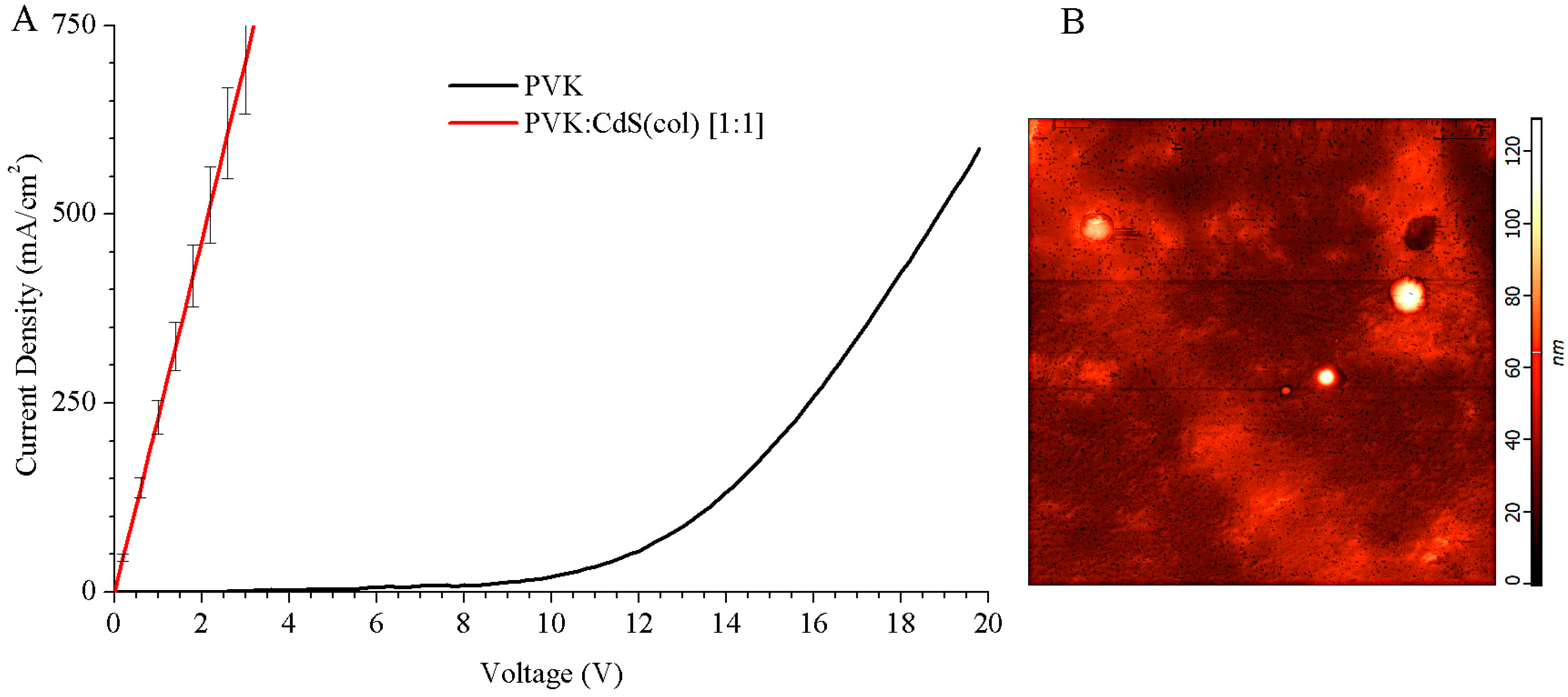
After device fabrication, we measured the current density—voltage (J–V) curves. In addition, electroluminescence (EL) characterization was performed.
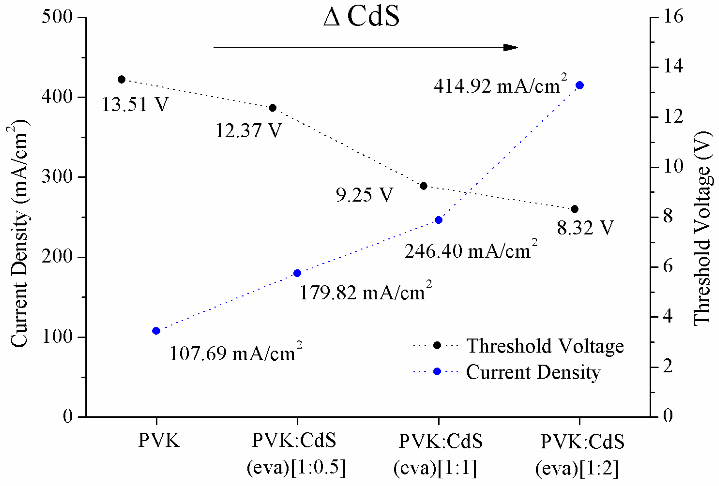
In the J–V curves (
Figure 11A), it is observed that at the same voltage values, the current density increases with the inclusion of nanoparticles. The improvement is proportional to the nanoparticles increase. The evaporated CdS NCs reduce the threshold voltage (
Figure 12) that is the lowest for the device with PVK:CdS ratio [1:2] and it is the highest for the LED without CdS NCs. At the same time,
Figure 12 shows the current density measured at the threshold voltage. The electronic transport in these devices improves with the presence of nanoparticles.
In devices with pristine PVK active layer, the potential barrier for electrons injection is 2 eV. As represented in
Figure 13, the PVK lowest unoccupied molecular orbital (LUMO) is located at −2.3 eV and for aluminium is −4.3 eV [
39]. Embedding CdS NCs in the polymer matrix decreases the energy barrier for electron injection. On the basis of the effective mass approximation the electron affinity of CdS NCs depends mostly on the energy of the conduction band edge. The band gap for the evaporated CdS NCs, calculated from optical absorption, is 2.65 eV (
Table 1). If the valence band edge of CdS is set on −6.8 eV relative to the vacuum level, then the energy level of the conduction band would shift up to −4.15 eV, much closer to the aluminium work function than the PVK LUMO. This approach causes the improvement of electrical conduction. Besides, electrons move through CdS conduction band with enhanced electron transport properties than those through PVK. The extension of the areas with potential closer to aluminium, increases with the ratio of CdS nanoparticles in the active layer, improving the electrical conduction with the nanocrystals content. In the hybrid LEDs of
Section 3.3, with colloidal CdS nanoparticles in DMSO solution their conduction band would be located at −3.55 eV and the potential barrier would not be so close to aluminium as with evaporated CdS. Therefore, the electronic transport of the hybrid LED with evaporated nanoparticles presents electrical improvements compared to LEDs with colloidal CdS NCs. In addition, although the TGA analysis indicates that nanoparticles do not suffer alterations due to the temperature, previous TEM and optical characterization analysis indicated that several thiols may have been released from the nanoparticles. This absence of ligands favours a direct connection between PVK and the CdS core, improving the electrical behaviour.
AFM analysis was performed also for these devices with free-DMSO CdS NCs. A portion of the surface of the LED with PVK:CdS [1:2] is shown in
Figure 11B. The tiny craters and circular monticules present in the devices with hybrid PVK:CdS(col) NCs layers (
Figure 4B) are not observed in LEDs with evaporated CdS nanoparticles. Extensive agglomerations of nanoparticles are visible on the surface of the device instead, especially in this device that had the higher NCs filling factor (theoretically 66.6% of the layer weight). Although the roughness of the surface is important these devices presented electroluminescent emission as it is shown in
Figure 14.
The efficiency of pristine PVK LED was 0.69 cd/A while for hybrid-LEDs doped with CdS NCs were 0.13 cd/A for [1:0.5], 0.09 cd/A for [1:1] and 0.06 cd/A for PVK:CdS(eva) [1:2]. The efficiencies showed that the nanocrystals reduce the external current conversion, as anticipated before [
12,
25,
26]. Agglomeration of NCs, as observed in AFM images (
Figure 11B), leads to inefficient energy transfer between the PVK matrix and thiophenol capped CdS NCs reducing luminescence efficiency [
38].
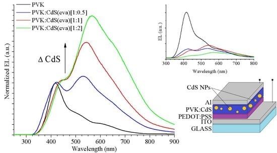
Electroluminescence measurements were carried out to PVK reference and to hybrid PVK:CdS LEDs (
Figure 14) in the same conditions used for LEDs in
Section 3.3. The inclusion of nanoparticles in the active layer caused a decrease in the integrated emission intensity of electroluminescence, as observed in the inset of
Figure 14.
For the PVK reference device, a narrow distinct peak at 412 nm wavelength is easily observed. As explained by Ye et al. [
40], PVK is a strongly polar polymer. The presence of an electrical field in electroluminescence characterization enhances the predominance of the fully overlapping conformation of carbazole groups (f-PVK), where both carbazole groups are aligned face-to-face in adjacent positions along the polymer backbone. This emission energy is slightly reduced, in comparison to that from photoluminescence, due to the shortened intermolecular distance in f-PVK conformation. This explains the red shift compared with former PVK photoluminescence emission.
Additionally, next to the main emission peak, two shoulders are perceived at longer wavelengths in the EL curve of the PVK LED (black curve in
Figure 14).
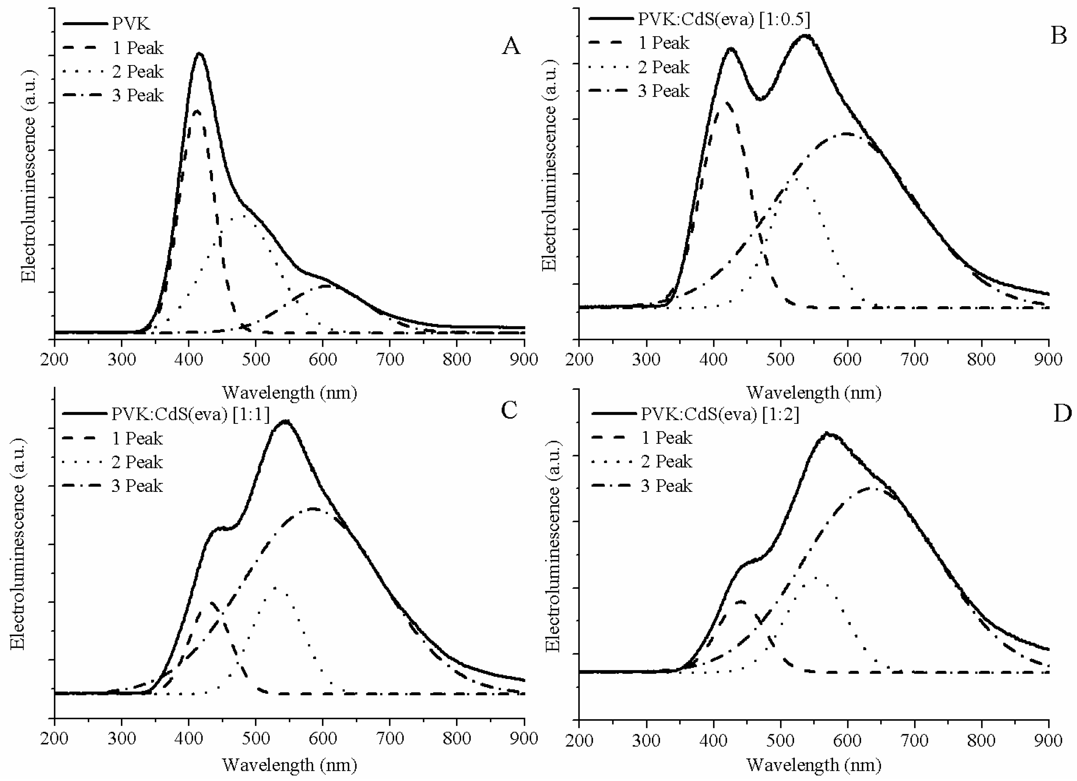
In order to clearly obtain the position of the peaks contributing to each EL curve, Gaussian deconvolution was performed for each spectrum (see
Figure 15). Three differentiated peaks were allowed to describe each EL curve. In
Table 3, the central wavelengths of the peaks obtained from the Gaussian deconvolutions have been collected.
The higher shoulder registered for the reference PVK device comes from the phosphorescence emission of the polymer [
40]. For EL processes the proportion of triplet states is increased compared to PL processes, this allows the observation of phosphorescent emissions at room temperature. For the device shown in
Figure 15A this emission was located at 477 nm according to our Gaussian simulation.
Finally, the lower shoulder observed in PVK EL spectrum is attributed to the electromer of PVK [
40]. This emission is only visible in EL, not in PL, because photoexcitation does not normally generate the free charge carriers needed to form this complex.
Regarding the electroluminescence from the hybrid LEDs with CdS evaporated NCs, we also observed three contributions, which we have correlated by means of the Gaussian deconvolution (see
Figure 15B–D).
The peak located at shorter wavelengths is coming from the PVK matrix emission. Its contribution to the whole electroluminescence goes down when the ratio of CdS NCs is increased. There are two main reasons for this expected behaviour: one just related to the lower amount of polymer present in the emissive layer when the mass of NCs increases, and the other is related to the quenching of PVK luminescence [
41]. As can be observed in
Figure 13 the energy difference between the conduction band of CdS NCs and the LUMO of PVK host is close to 2 eV hindering the flow of electrons towards the polymer. Thus the electroluminescence quenching might also be ascribed to the electron-trap role of the CdS NCs.
The highest peak and the shoulder observed at longer wavelengths in hybrid EL spectra are due to CdS NCs emission as can be guessed looking at
Figure 14, where the increase of these contributions is noticeable along with the ratio of CdS NCs embedded in the devices.
As we have previously observed in TEM evaluation, after evaporation, some CdS NCs have grown up and changed their crystalline structure evolving from cubic to hexagonal structure. Through Gaussian deconvolution we are able to link the stronger emission from bigger CdS NCs with the longer wavelength shoulder (close to 600 nm) of EL spectra, and the weaker contribution of cubic CdS NCs, adding to raise the EL emission to its maximum intensity at wavelengths around 550 nm for the hybrid LEDs.
Thus the second peak obtained from the Gaussian deconvolution for the hybrid LEDs, is attributed to the CdS NCs that have suffered a minimum alteration after the drying process. It corresponds to the smaller CdS nanocrystals that hold on the cubic structure. This emission is assumed in the range between 524 and 552 nm (
Table 3) for the LEDs shown in
Figure 14 and
Figure 15. There is some red-shift compared to the photoluminescence emission of the CdS NCs synthesized in DMSO (
Figure 1 and
Figure 2) but this is expected for electroluminescence, which is produced by different mechanisms than photo induced luminescence [
42].
Finally, we assign the Gaussian curve responsible of the shoulder observed at longer wavelengths in the EL spectra of hybrid LEDs to emission from the larger size evaporated CdS NCs with hexagonal crystalline structure. This is the main contribution to the electroluminescence of these devices. The electroluminescence of these larger NCs is also slightly red-shifted if we contrast with the photoluminescence emission registered around 590 nm in
Figure 6 and
Figure 11. The wide Full Width at Half Maximum (FWHM) might be caused by the high size dispersion that we have demonstrated by TEM study.
In order to further demonstrate this hypothesis instead of the well-known identification of the middle peak (located around 540 nm) as the CdS NCs band-gap emission, and the longer wavelength band (located around 600 nm) as the emission related to traps located in the NC surface, we analysed the electroluminescence as a function of voltage (see
Figure S1 in Supplementary Information). We have checked that both peaks related to NCs follow similar trends with increased voltage. Moreover, we do not observe saturation on the emission of the longer wavelength peak at higher voltages. On the contrary, it increases slightly its influence on the emission at higher applied voltages. Based on all these evidences, we corroborate the validity of our argument against the expected band-gap and related traps emission.
In addition, we studied the CIE 1931 chromaticity for the hybrid-LEDs fabricated (see
Figure S2 in Supplementary Information). The color coordinates for PVK-LED were (0.24, 0.22). Increasing loading of CdS NCs modified the CIE coordinates of PVK LED towards near-white color CIE coordinates (0.33, 0.33) [
21]. The chromatic coordinates were: (0.32, 0.34) for PVK:CdS [1:0.5]; (0.34, 0.38) for PVK:CdS [1:1] and (0.38, 0.39) for PVK:CdS [1:2]. Increments of CdS reduced the influence of PVK, as a result, the CIE coordinates were shifted by the presence of CdS NCs towards the coordinates of CdS NCs light emission (0.43, 0.45).


