Probing the Field-Effect Transistor with Monolayer MoS2 Prepared by APCVD


Abstract
:1. Introduction
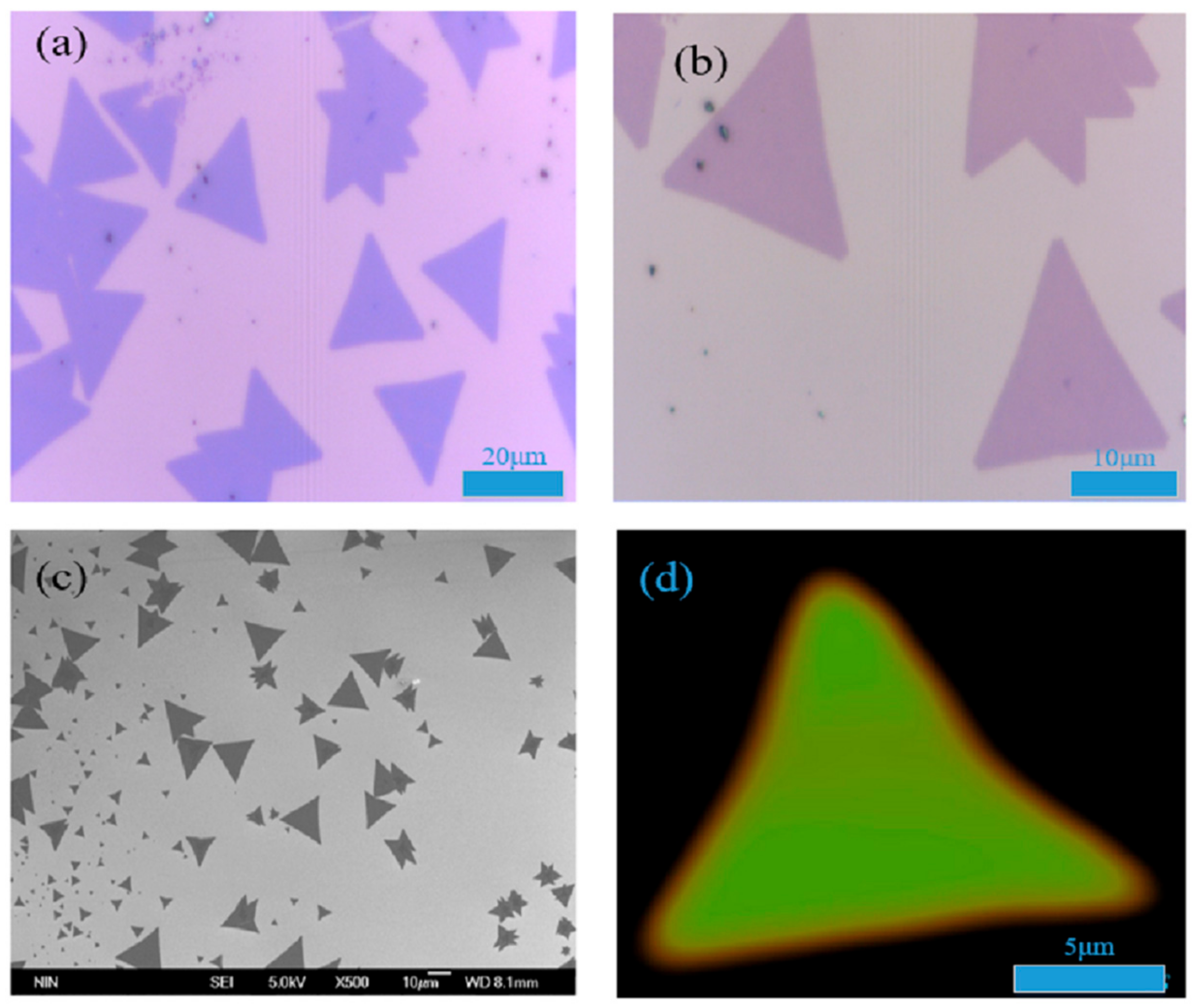
2. The Growth and Characterization of Monolayer MoS2
2.1. The Growth Process of Monolayer MoS2
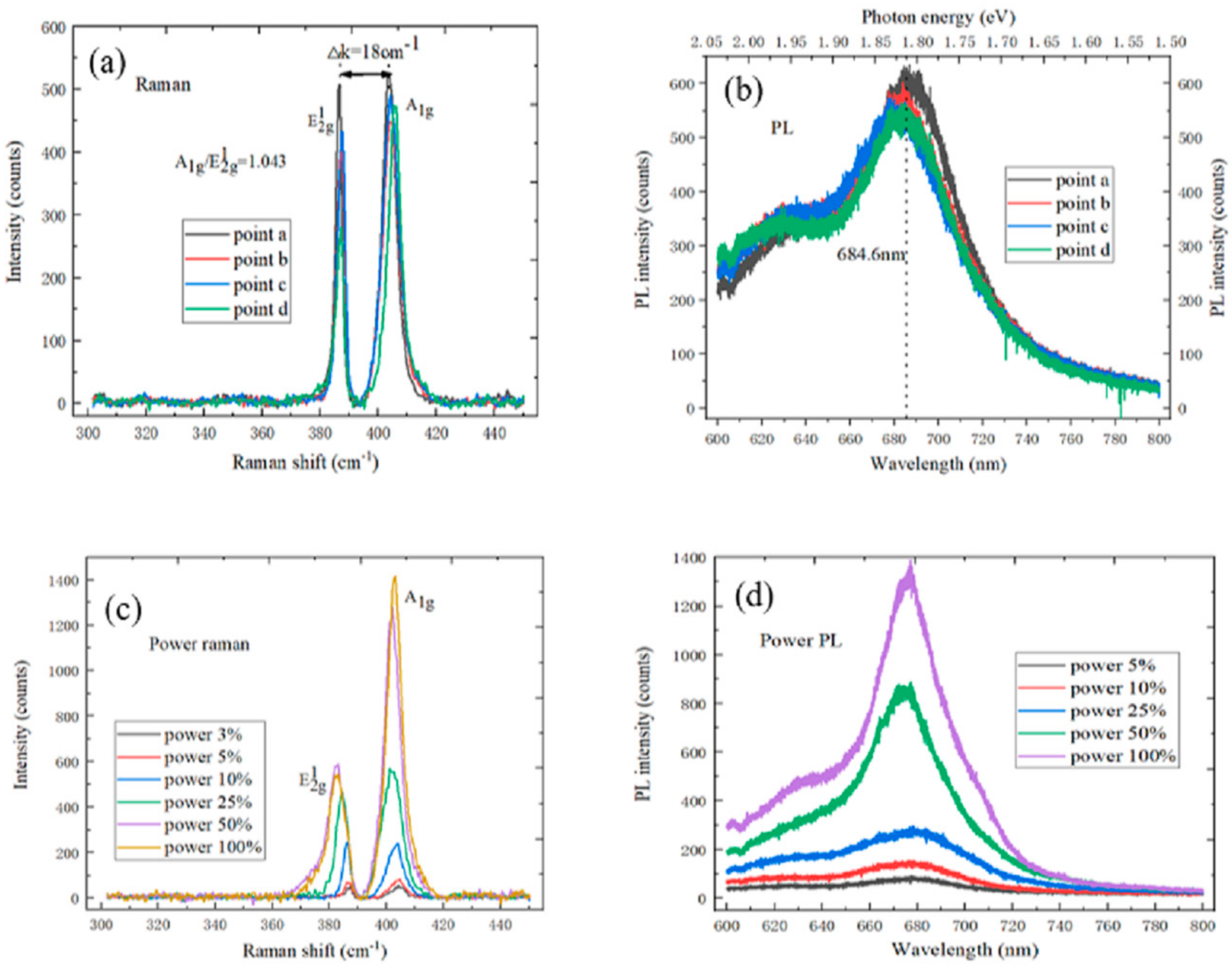
2.2. The Test Characterization Conditions of Monolayer MoS2
3. The Discussion of Electrical Performance Results
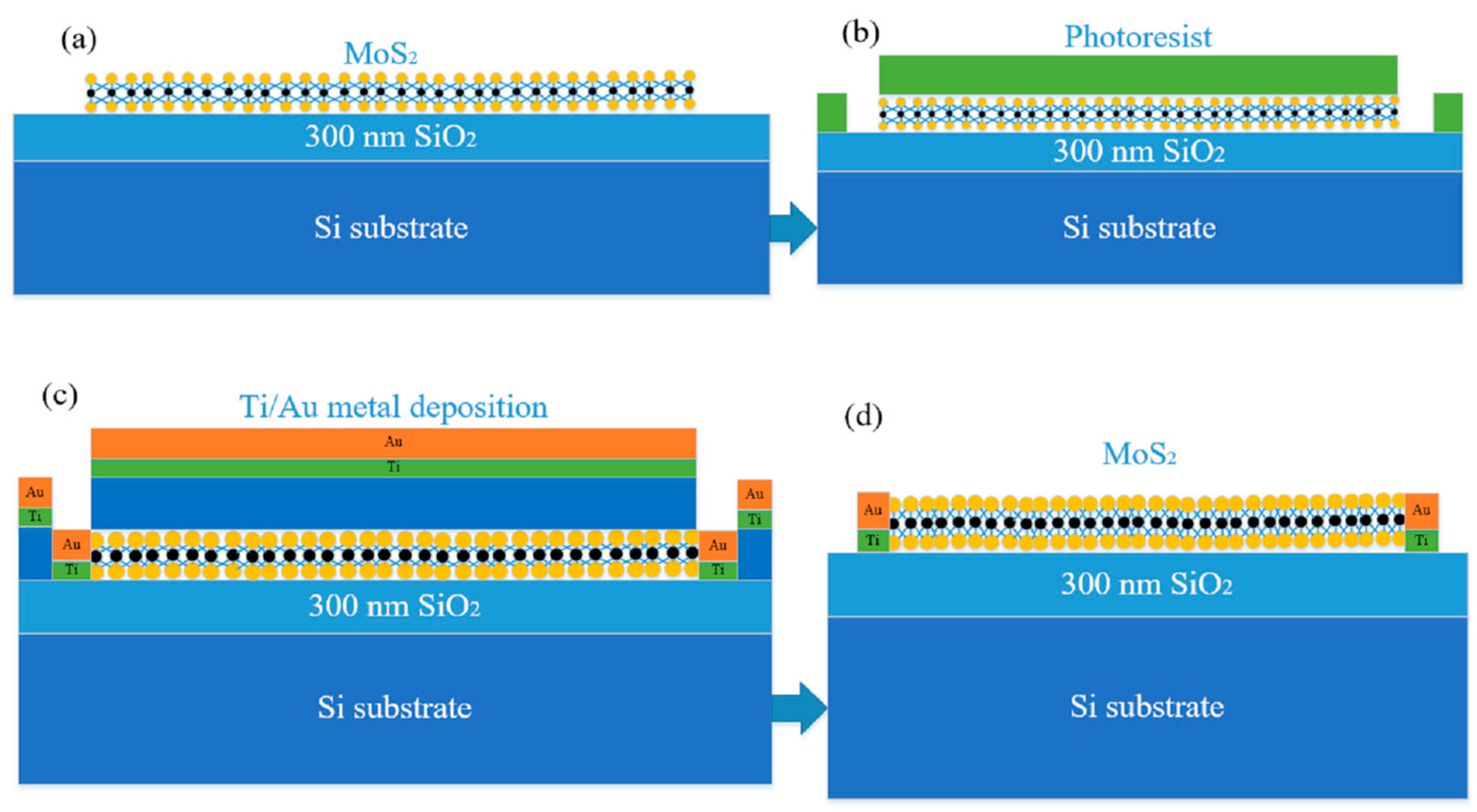
3.1. The Fabrication Process of Monolayer MoS2-Based FET
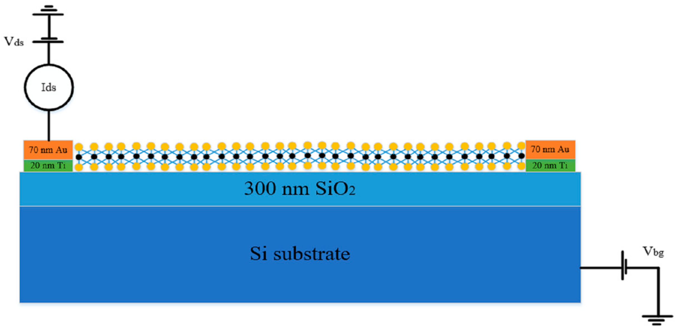
3.2. The Electrical Properties of Monolayer MoS2-Based FET
4. Conclusions
Author Contributions
Funding
Conflicts of Interest
References
- Lin, M.-W.; Kravchenko, I.; Fowlkes, J.; Li, X.; Puretzky, A.; Rouleau, C.M.; Geohegan, D.B.; Xiao, K. Thickness-dependent charge transport in few-layer MoS2 field-effect transistors. Nanotechnology 2016, 27, 165203. [Google Scholar] [CrossRef] [PubMed]
- Chae, W.H.; Cain, J.D.; Hanson, E.D.; Murthy, A.A.; Dravid, V.P. Substrate-induced strain and charge doping in CVD-grown monolayer MoS2. Appl. Phys. Lett. 2017, 111, 143106. [Google Scholar] [CrossRef]
- Momeni, K.; Ji, Y.; Zhang, K.; Robinson, J.A.; Chen, L.-Q. Multiscale framework for simulation-guided growth of 2D materials. NPJ 2D Mater. Appl. 2018, 2, 27. [Google Scholar] [CrossRef]
- Zhu, H.; Wang, X.; Zhang, T.-B.; Yang, W.; Chen, L.; Sun, Q.-Q.; Zhang, D.W. Improved integration of ultra-thin high-k dielectrics in few-layer MoS2 FET by remote forming gas plasma pretreatment. Appl. Phys. Lett. 2017, 110, 053110. [Google Scholar]
- Zubair, A.; Sajjad, R.N.; Tavakkoli, K.G.A.; Fang, S.; Ling, X.; Kong, J.; Dresselhaus, M.S.; Kaxiras, E.; Berggren, K.K.; Antoniadis, D.; et al. MoS2 Field-Effect Transistor with Sub-10-nm Channel Length. Nano Lett. 2016, 16, 7798–7806. [Google Scholar]
- Xu, H.; Zhou, W.; Zheng, X.; Huang, J.; Feng, X.; Ye, L.; Xu, G.; Lin, F. Control of the nucleation density of molybdenum disulfide in large-scale synthesis using chemical vapor deposition. Materials 2018, 11, 870. [Google Scholar] [CrossRef] [PubMed]
- Sanne, A.; Ghosh, R.; Rai, A.; Yogeesh, M.N.; Shin, S.H.; Sharma, A.; Jarvis, K.; Mathew, L.; Rao, R.; Akinwande, D.; et al. Radio Frequency Transistors and Circuits Based on CVD MoS2. Nano Lett. 2015, 15, 5039–5045. [Google Scholar] [CrossRef] [PubMed]
- Han, T.; Liu, H.; Wang, S.; Li, W.; Chen, S.; Yang, X.; Cai, M. Research on the Factors Affecting the Growth of Large-Size Monolayer MoS2 by APCVD. Materials 2018, 11, 2562. [Google Scholar] [CrossRef] [PubMed]
- Liu, H.; Neal, A.T.; Ye, P.D. Channel Length Scaling of MoS2 MOSFETs. ACS Nano 2012, 6, 8563–8569. [Google Scholar] [CrossRef]
- Zafar, A.; Nan, H.; Zafar, Z.; Wu, Z.; Jiang, J.; You, Y.; Ni, Z. Probing the intrinsic optical quality of CVD grown MoS2. Nano Res. 2017, 10, 1608–1617. [Google Scholar] [CrossRef]
- Li, X.; Zhu, H. Two-dimensional MoS2: Properties, preparation, and applications. J. Mater. 2015, 1, 33–44. [Google Scholar] [CrossRef]
- Wang, J.; Yao, Q.; Huang, C.-W.; Zou, X.; Liao, L.; Chen, S.; Fan, Z.; Zhang, K.; Wu, W.; Xiao, X.; et al. High Mobility MoS2 Transistor with Low Schottky Barrier Contact by Using Atomic Thick h-BN as a Tunneling Layer. Adv. Mater. 2016, 28, 8302–8308. [Google Scholar] [CrossRef] [PubMed]
- Xu, W.; Li, S.; Zhou, S.; Lee, J.K.; Wang, S.; Sarwat, S.G.; Wang, X.; Bhaskaran, H.; Pasta, M.; Warner, J.H. Large Dendritic Monolayer MoS2 Grown by Atmospheric Pressure Chemical Vapor Deposition for Electrocatalysis. ACS Appl. Mater. Interfaces 2018, 10, 4630–4639. [Google Scholar] [CrossRef] [PubMed]
- Di Bartolomeo, A.; Genovese, L.; Foller, T.; Giubileo, F.; Luongo, G.; Croin, L.; Liang, S.-J.; Ang, L.K.; Schleberger, M. Electrical transport and persistent photoconductivity in monolayer MoS2 phototransistors. Nanotechnology 2017, 28, 214002. [Google Scholar] [CrossRef] [PubMed]
- Das, S.; Demarteau, M.; Roelofs, A. Nb-doped single crystalline MoS2 field effect transistor. Appl. Phys. Lett. 2015, 106, 173506. [Google Scholar] [CrossRef]
- Chen, T.; Zhou, Y.; Sheng, Y.; Wang, X.; Zhou, S.; Warner, J.H. Hydrogen-Assisted Growth of Large-Area Continuous Films of MoS2 on Monolayer Graphene. ACS Appl. Mater. Interfaces 2018, 10, 7304–7314. [Google Scholar] [CrossRef]
- Bhattacharjee, S.; Ganapathi, K.L.; Mohan, S.; Bhat, N. A sub-thermionic MoS2 FET with tunable transport. Appl. Phys. Lett. 2017, 111, 163501. [Google Scholar] [CrossRef]
- Zhang, F.; Appenzeller, J. Tunability of Short-Channel Effects in MoS2 Field-Effect Devices. Nano Lett. 2014, 15, 301–306. [Google Scholar] [CrossRef]
- Han, T.; Liu, H.; Wang, S.; Chen, S.; Li, W.; Yang, X. Probing the Growth Improvement of Large-Size High Quality Monolayer MoS2 by APCVD. Nanotechnology 2019, 9, 433. [Google Scholar] [CrossRef]
- Bhattacharjee, S.; Ganapathi, K.L.; Nath, D.N.; Bhat, N. Intrinsic limit for contact resistance in exfoliated multilayered MoS2 FET. IEEE Electron Device Lett. 2015, 37, 119–122. [Google Scholar] [CrossRef]
- Kim, C.-K.; Yu, C.H.; Hur, J.; Bae, H.; Jeon, S.-B.; Park, H.; Choi, K.C. Abnormal electrical characteristics of multi-layered MoS2 FETs attributed to bulk traps. 2D Mater. 2016, 3, 15007. [Google Scholar] [CrossRef]
- Zhang, Y.; Xu, L.; Walker, W.R.; Tittle, C.M.; Backhouse, C.J.; Pope, M.A. Langmuir films and uniform, large area, transparent coatings of chemically exfoliated MoS2 single layers. J. Mater. Chem. C 2017, 5, 11275–11287. [Google Scholar] [CrossRef]
- Amani, M.; Chin, M.L.; Birdwell, A.G.; O’Regan, T.P.; Najmaei, S.; Liu, Z.; Ajayan, P.M.; Lou, J.; Dubey, M. Electrical performance of monolayer MoS2 field-effect transistors prepared by chemical vapor deposition. Appl. Phys. Lett. 2013, 102, 193107. [Google Scholar] [CrossRef]
- Li, Z.; Ye, R.; Feng, R.; Kang, Y.; Zhu, X.; Tour, J.M.; Fang, Z. Graphene quantum dots doping of MoS2 monolayers. Adv. Mater. 2015, 27, 5235–5240. [Google Scholar] [CrossRef] [PubMed]
- Strojnik, M.; Kovic, A.; Mrzel, A.; Buh, J.; Strle, J.; Mihailovic, D. MoS2 nanotube field effect transistors. AIP Adv. 2014, 4, 97114. [Google Scholar] [CrossRef]
- Yu, F.; Liu, Q.; Gan, X.; Hu, M.; Zhang, T.; Li, C.; Kang, F.; Terrones, M.; Lv, R. Ultrasensitive Pressure Detection of Few-Layer MoS2. Adv. Mater. 2017, 29, 1603266. [Google Scholar] [CrossRef] [PubMed]
- Chang, H.Y.; Yogeesh, M.N.; Ghosh, R.; Rai, A.; Sanne, A.; Yang, S.; Lu, N.; Banerjee, S.K.; Akinwande, D. Large-Area Monolayer MoS2 for Flexible Low-Power RF Nanoelectronics in the GHz Regime. Adv. Mater. 2016, 28, 1818–1823. [Google Scholar] [CrossRef]
- Li, X.; Li, X.; Zang, X.; Zhu, M.; He, Y.; Wang, K.; Xie, D.; Zhu, H. Role of hydrogen in the chemical vapor deposition growth of MoS2 atomic layers. Nanoscale 2015, 7, 8398–8404. [Google Scholar] [CrossRef]
- Liu, F.; Wang, J.; Wang, L.; Cai, X.; Jiang, C.; Wang, G. Enhancement of photodetection based on perovskite/MoS2 hybrid thin film transistor. J. Semicond. 2017, 38, 34002. [Google Scholar] [CrossRef]
- Chow, P.K.; Singh, E.; Viana, B.C.; Gao, J.; Luo, J.; Li, J.; Lin, Z.; Elías, A.L.; Shi, Y.; Wang, Z. Wetting of mono and few-layered WS2 and MoS2 films supported on Si/SiO2 substrates. ACS Nano 2015, 9, 3023–3031. [Google Scholar] [CrossRef]
- Kang, J.; Liu, W.; Banerjee, K. High-performance MoS2 transistors with low-resistance molybdenum contacts. Appl. Phys. Lett. 2014, 104, 93106. [Google Scholar] [CrossRef]
- Li, H.; Yin, Z.; He, Q.; Li, H.; Huang, X.; Lu, G.; Fam, D.W.H.; Tok, A.I.Y.; Zhang, Q.; Zhang, H. Fabrication of single-and multilayer MoS2 film-based field-effect transistors for sensing NO at room temperature. Small 2012, 8, 63–67. [Google Scholar] [CrossRef] [PubMed]


© 2019 by the authors. Licensee MDPI, Basel, Switzerland. This article is an open access article distributed under the terms and conditions of the Creative Commons Attribution (CC BY) license (http://creativecommons.org/licenses/by/4.0/).
Share and Cite
Han, T.; Liu, H.; Wang, S.; Chen, S.; Xie, H.; Yang, K. Probing the Field-Effect Transistor with Monolayer MoS2 Prepared by APCVD. Nanomaterials 2019, 9, 1209. https://doi.org/10.3390/nano9091209
Han T, Liu H, Wang S, Chen S, Xie H, Yang K. Probing the Field-Effect Transistor with Monolayer MoS2 Prepared by APCVD. Nanomaterials. 2019; 9(9):1209. https://doi.org/10.3390/nano9091209
Chicago/Turabian StyleHan, Tao, Hongxia Liu, Shulong Wang, Shupeng Chen, Haiwu Xie, and Kun Yang. 2019. "Probing the Field-Effect Transistor with Monolayer MoS2 Prepared by APCVD" Nanomaterials 9, no. 9: 1209. https://doi.org/10.3390/nano9091209
APA StyleHan, T., Liu, H., Wang, S., Chen, S., Xie, H., & Yang, K. (2019). Probing the Field-Effect Transistor with Monolayer MoS2 Prepared by APCVD. Nanomaterials, 9(9), 1209. https://doi.org/10.3390/nano9091209