The Study of Deep Level Traps and Their Influence on Current Characteristics of InP/InGaAs Heterostructures

Abstract
:1. Introduction
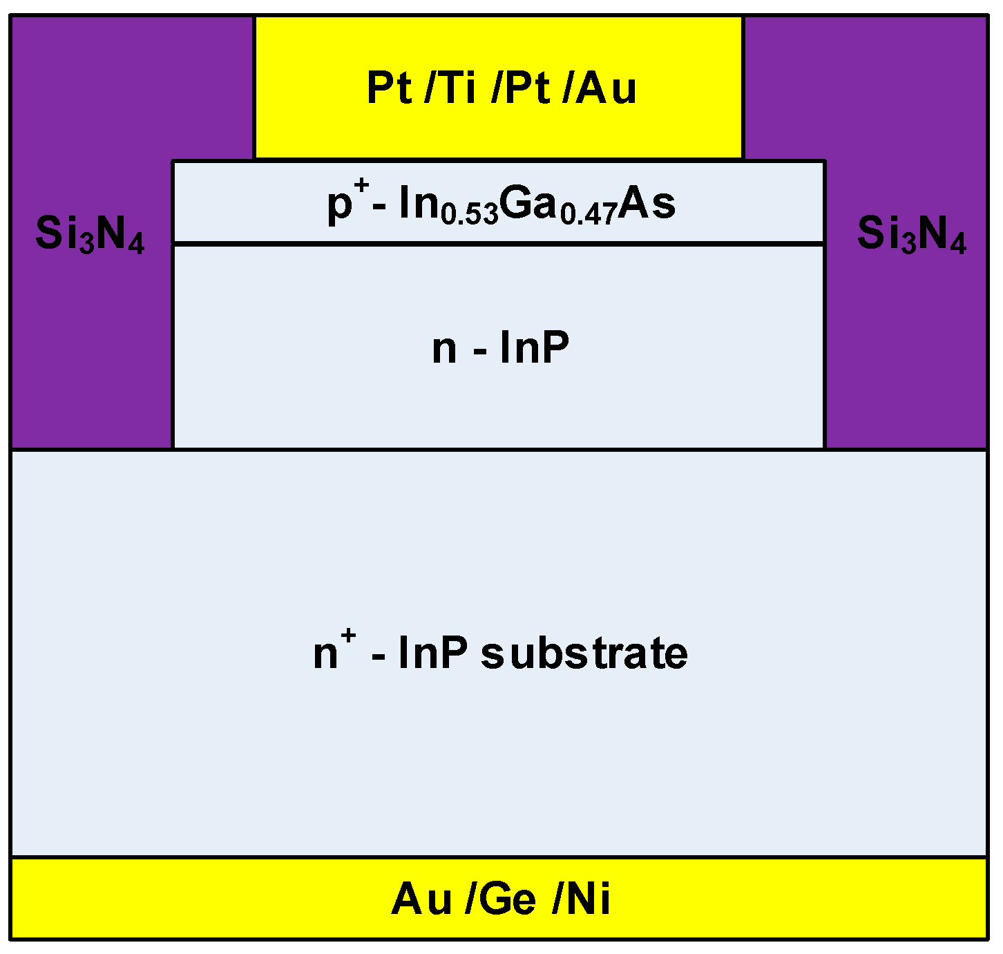
2. Experiments
3. Results and Discussion
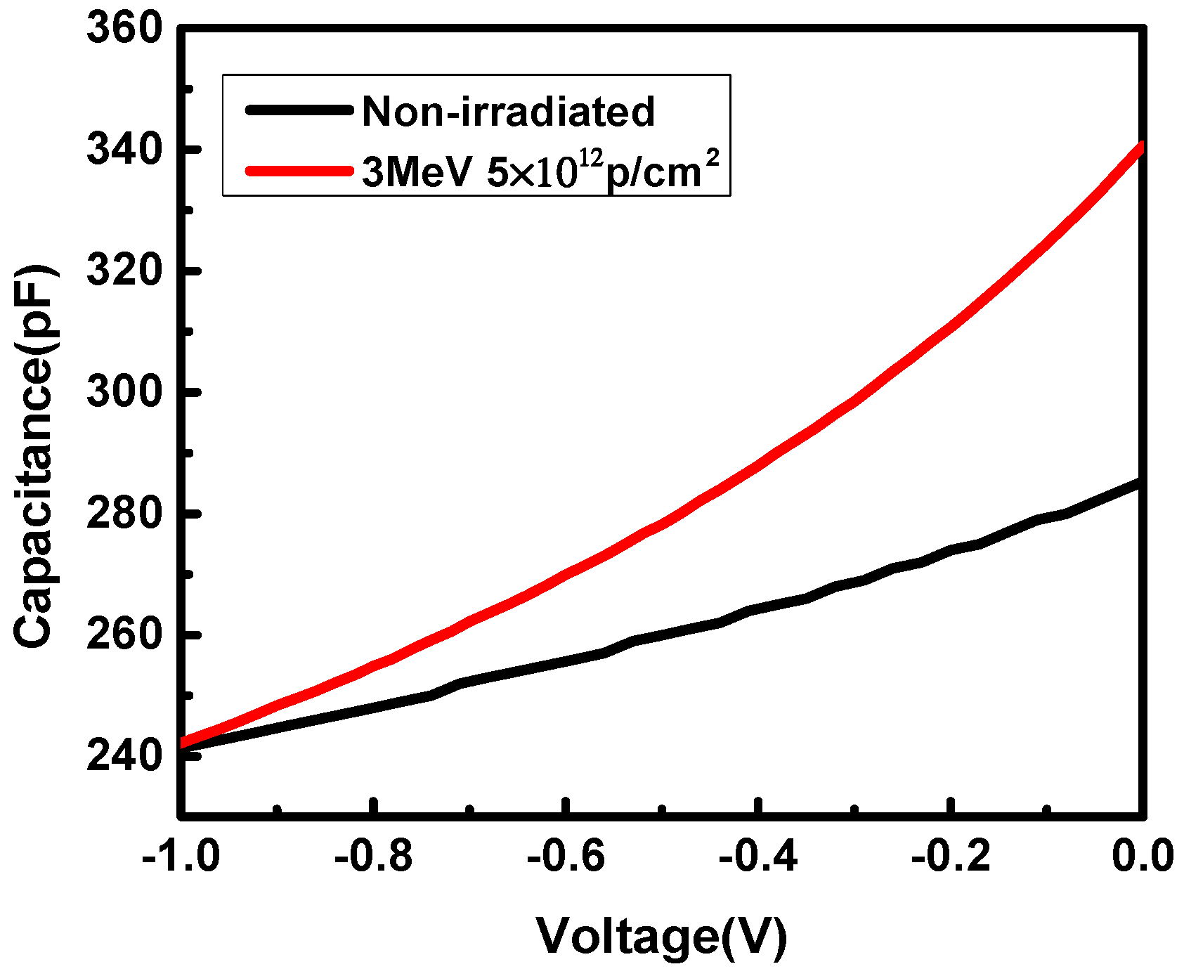
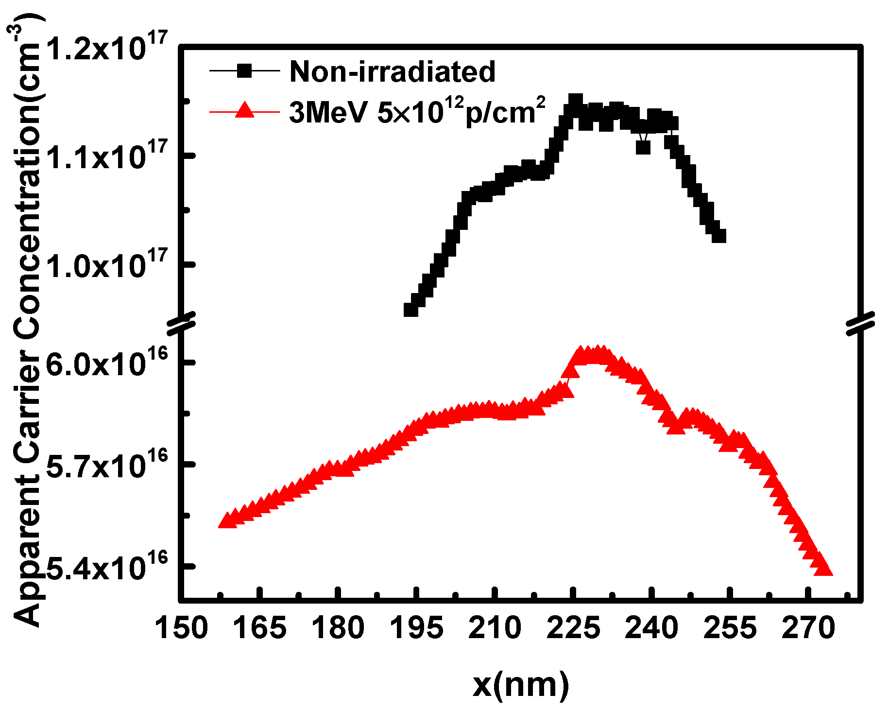
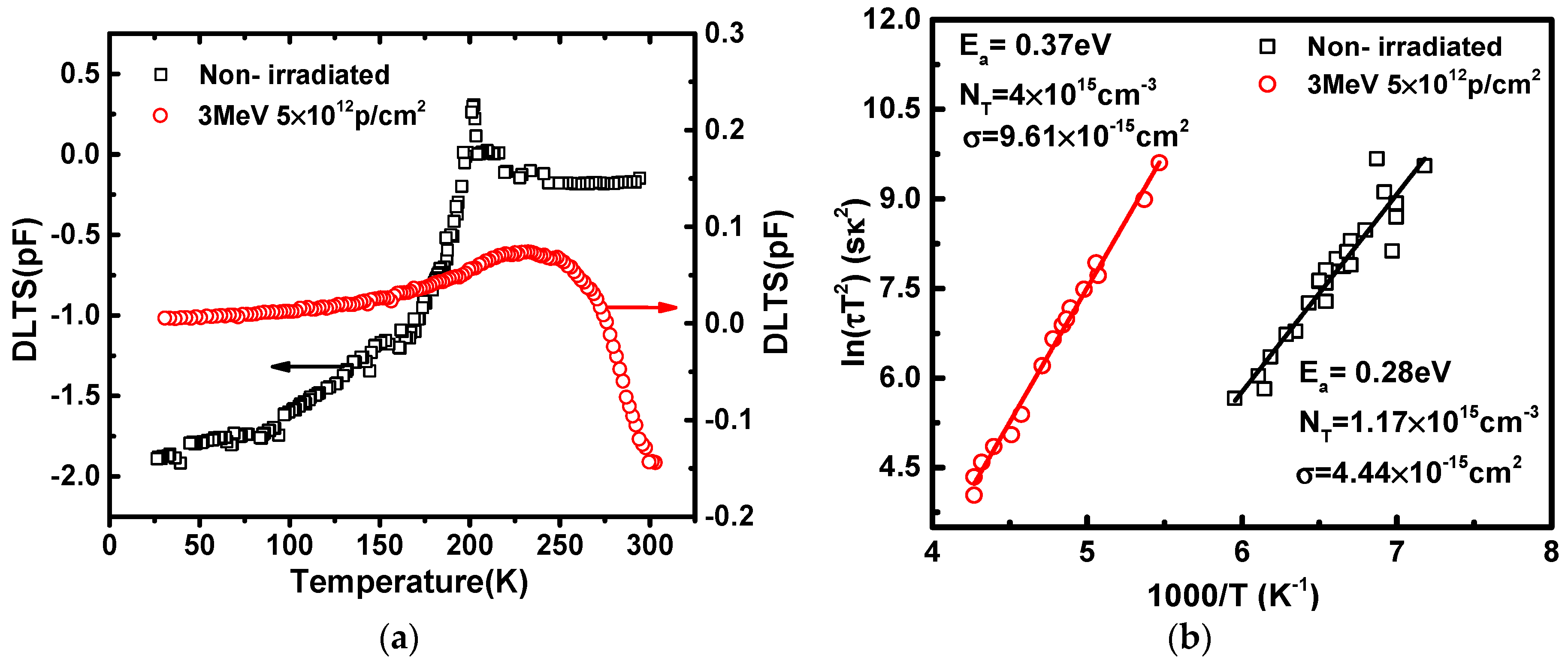
3.1. C–V and DLTS Measurements
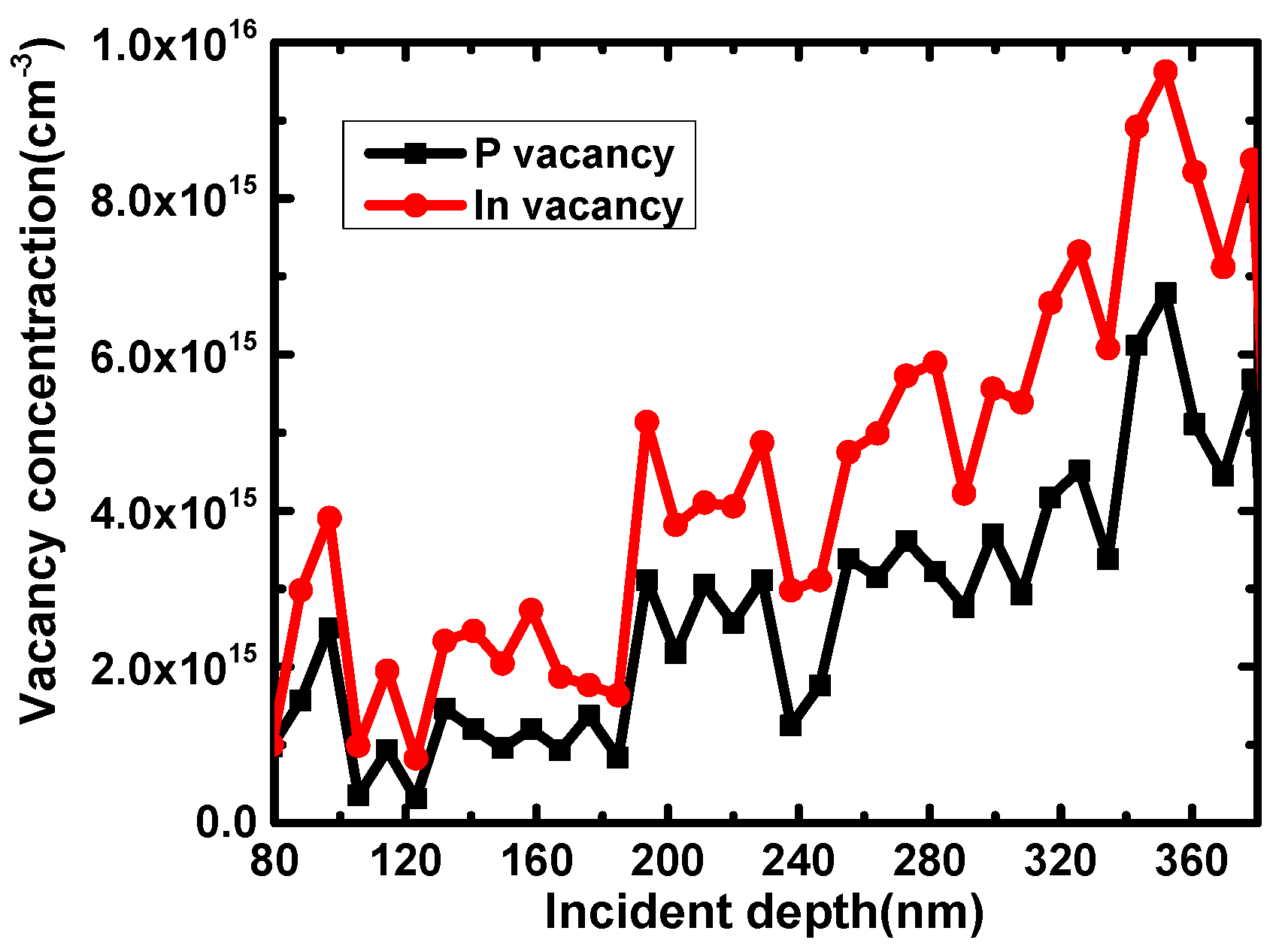
3.2. The Simulation of Proton Irradiation Damage by SRIM
3.3. The Effect of Deep Level Traps on Current Characteristics
4. Conclusions
Author Contributions
Funding
Acknowledgments
Conflicts of Interest
References
- Urteaga, M.; Griffith, Z.; Seo, M.; Hacker, J.; Rodwell, M.J. InP HBT technologies for THz integrated circuits. Proc. IEEE 2017, 105, 1051–1067. [Google Scholar] [CrossRef]
- Shatalov, A.; Subramanian, S.; Chandrasekhar, S.; Dentai, A.; Goodnick, S.M. Electron irradiation effects in polyimide passivated InP/InGaAs single heterojunction bipolar transistors. IEEE Trans. Nucl. Sci. 1999, 46, 1708–1715. [Google Scholar] [CrossRef]
- Shatalov, A.; Subramanian, S.; Dentai, A. Neutron irradiation effects in InP/InGaAs single heterojunction bipolar transistors. IEEE Trans. Nucl. Sci. 2000, 47, 2551–2556. [Google Scholar] [CrossRef]
- Liu, M.; Zhang, Y.; Lu, H.; Zhang, Y.; Zhang, J.; Ren, X. Investigation of proton irradiation effects on InP/InGaAs double heterojunction bipolar transistors. Solid-State Electron. 2015, 109, 52–57. [Google Scholar] [CrossRef]
- Shatalov, A.; Subramanian, S.; Dentai, A.; Chadrasekhar, S.; Goodnick, S.M. Neutron irradiation induced degradation of the collector–emitter offset voltage in InP/InGaAs single heterojunction bipolar transistors. J. Appl. Phys. 2000, 88, 3765–3767. [Google Scholar] [CrossRef]
- Shatalov, A. Radiation Effects in III-V Semiconductors and Heterojunction Bipolar Transistors. Ph.D. Thesis, Oregon State University, Corvallis, OR, USA, 2001. [Google Scholar]
- Li, C.H.; Lu, H.L.; Zhang, Y.M.; Liu, M.; Zhao, X.H. Proton-Induced Degradation of InP/InGaAs HBTs Predicted by Nonionizing Energy Loss Model. IEEE Trans. Nucl. Sci. 2015, 62, 1336–1340. [Google Scholar] [CrossRef]
- Kroemer, H. Determination of heterojunction band offsets by capacitance-voltage profiling through nonabrupt isotype heterojunctions. Appl. Phys. Lett. 1985, 46, 504–505. [Google Scholar] [CrossRef]
- Rao, M.A.; Caine, E.J.; Kroemer, H. Determination of valence and conduction–band discontinuities at the (Ga, In) P/GaAs heterojunction by C–V profiling. J. Appl. Phys. 1987, 61, 643–649. [Google Scholar] [CrossRef]
- Lehovec, K. C–V analysis of a partially depleted semiconducting channel. Appl. Phys. Lett. 1975, 26, 82–84. [Google Scholar] [CrossRef]
- Nelson, I.V.; Thomas, G. Native and Radiation-Induced Defects in III-V Solar Cells and Photodiodes. Ph.D. Thesis, Rochester University, New York, NY, USA, 2019. [Google Scholar]
- Chen, X.Y.; Zhang, Y.G.; Gu, Y. Analysis of dark currents and deep level traps in InP-and GaAs-based In0.83Ga0.17As photodetectors. J. Cryst. Growth 2017, 477, 82–85. [Google Scholar] [CrossRef]
- Weiss, S.; Kassing, R. Deep Level Transient Fourier Spectroscopy (DLTFS)—A technique for the analysis of deep level properties. Solid-State Electron. 1988, 31, 1733–1742. [Google Scholar] [CrossRef]
- McAfee, S.R.; Capasso, F.; Lang, D.V.; Hutchinson, A.; Bonner, W.A. A study of deep level in bulk n-InP by transient spectroscopy. J. Appl. Phys. 1981, 52, 6158–6164. [Google Scholar] [CrossRef]
- Wang, C.; Simoen, E.; AliReza, A.; Sioncke, S.; Collaert, N.; Claeys, C.; Li, W. Deep level investigation of INGAAS on INP layer. In Proceedings of the China Semiconductor Technology International Conference (CSTIC), Shanghai, China, 12–13 March 2017; IEEE. pp. 1–4. [Google Scholar]
- Sze, S.M.; Ng, K.K. Physics of Semiconductor Devices; John Wiley & Sons: Hoboken, NJ, USA, 2006. [Google Scholar]


| Proton Irradiation | DLTS | C–V | SRIM | ||
|---|---|---|---|---|---|
| 3 MeV 5 × 10¹² p/cm2 | Ea | σ | NT | σi | Vacancy |
| 0.37 eV | 9.61 × 10⁻¹⁵ cm2 | 4 × 1015 cm−3 | 1.8 × 1012 cm−2 | 4.18 × 1015 cm−3 | |
© 2019 by the authors. Licensee MDPI, Basel, Switzerland. This article is an open access article distributed under the terms and conditions of the Creative Commons Attribution (CC BY) license (http://creativecommons.org/licenses/by/4.0/).
Share and Cite
Zhao, X.; Lu, H.; Zhao, M.; Zhang, Y.; Zhang, Y. The Study of Deep Level Traps and Their Influence on Current Characteristics of InP/InGaAs Heterostructures. Nanomaterials 2019, 9, 1141. https://doi.org/10.3390/nano9081141
Zhao X, Lu H, Zhao M, Zhang Y, Zhang Y. The Study of Deep Level Traps and Their Influence on Current Characteristics of InP/InGaAs Heterostructures. Nanomaterials. 2019; 9(8):1141. https://doi.org/10.3390/nano9081141
Chicago/Turabian StyleZhao, Xiaohong, Hongliang Lu, Manli Zhao, Yuming Zhang, and Yimen Zhang. 2019. "The Study of Deep Level Traps and Their Influence on Current Characteristics of InP/InGaAs Heterostructures" Nanomaterials 9, no. 8: 1141. https://doi.org/10.3390/nano9081141
APA StyleZhao, X., Lu, H., Zhao, M., Zhang, Y., & Zhang, Y. (2019). The Study of Deep Level Traps and Their Influence on Current Characteristics of InP/InGaAs Heterostructures. Nanomaterials, 9(8), 1141. https://doi.org/10.3390/nano9081141