Article

Effect of Electron Irradiation Fluence on InP-Based High Electron Mobility Transistors

1
School of Physics and Engineering, Zhengzhou University, Zhengzhou 450001, China
2
Institute of Microelectronics, Chinese Academy of Sciences, Beijing 100029, China
3
China Academy of Space Technology, Beijing 100086, China
*
Author to whom correspondence should be addressed.
These authors contributed equally to this work.
Nanomaterials 2019, 9(7), 967; https://doi.org/10.3390/nano9070967
Submission received: 26 May 2019 / Revised: 25 June 2019 / Accepted: 27 June 2019 / Published: 1 July 2019

Abstract

:
In this paper, the effect of electron irradiation fluence on direct current (DC) and radio frequency (RF) of InP-based high electron mobility transistors (HEMTs) was investigated comprehensively. The devices were exposed to a 1 MeV electron beam with varied irradiation fluences from 1 × 1014 cm−2, 1 × 1015 cm−2, to 1 × 1016 cm−2. Both the channel current and transconductance dramatically decreased as the irradiation fluence rose up to 1 × 1016 cm−2, whereas the specific channel on-resistance (Ron) exhibited an apparent increasing trend. These changes could be responsible for the reduction of mobility in the channel by the irradiation-induced trap charges. However, the kink effect became weaker with the increase of the electron fluence. Additionally, the current gain cut-off frequency (fT) and maximum oscillation frequency (fmax) demonstrated a slightly downward trend as the irradiation fluence rose up to 1 × 1016 cm−2. The degradation of frequency properties was mainly due to the increase of gate-drain capacitance (CGD) and the ratio of gate-drain capacitance and gate-source capacitance (CGD/CGS). Moreover, the increase of Ron may be another important factor for fmax reduction.

1. Introduction

With the development of high-precision detection and high-speed data transmission applications, the operating frequency of the core chips in transceiver systems has increased from W band to G band and even terahertz [1,2,3]. Confined to physical constraint and manufacturing cost, the typical channel length of metal–oxide–semiconductor field-effect transistors (MOSFETs) is hard to downscale further after the 10 nm node. For nearly several decades, III-V compound semiconductor transistors have stood out and become competitive alternatives for devices based on either advanced micro/nano-fabrication technologies or novel structures [4,5,6]. Benefiting from electron beam lithography (EBL) and molecular beam epitaxy (MBE) techniques, the current gain cut-off frequency (fT) and maximum oscillation frequency (fmax) of InP-based high electron mobility transistors (HEMTs) have been reported to be over 700 GHz [7] and 1 THz [8], respectively. Therefore, InP-based HEMTs are potentially excellent candidates for various millimeter-wave circuits of transceiver systems in space applications, such as national defense, aerospace, and satellite radar [9].
Radiation tolerance is critical for semiconductor devices which operate in space missions [10]. In the space environment, various high-energy particles and rays damage electronic devices, resulting in performance degradation of the devices and even the abnormality of electronic systems [11,12]. Admittedly, the irradiation damage mechanism of various devices with III-V materials have been widely reported [13,14,15,16,17,18]. Oh et al. studied the effects of electron irradiation on the gate leakage current of AlGaN/GaN HEMTs. The results showed that the gate leakage current significantly decreased, which was due to the neutralization of nitrogen vacancies, and that the removal of oxygen impurities induced the defects after electron irradiation [14]. Kimura et al. performed a systematic study of electron irradiation effects on the Schottky gate of InGaAs/GaAs HEMTs which showed that deep traps were introduced at the gate metal and GaAs layer [15]. The impact of proton irradiation on the direct current (DC) performance of AlGaN/GaN HEMTs was investigated by Liu et al., which indicated that the DC characteristics were degraded more seriously at high proton fluence. This was due to the greater reduction of the electron concentration and mobility at high proton fluence [17]. Most of these research studies are focused mainly on GaN and GaAs materials. However, only a few articles have investigated the irradiation effects on InP-based HEMT devices, especially the effects on the Kink effect and radio frequency (RF) characteristics. Actually, electrons are major radiation particles in the low earth orbit, where many satellites and space stations are found. Incident electrons create lattice defects in semiconductor devices, such as vacancies, interstitials, and complex defects, which are induced by atomic displacements [19]. Moreover, electron irradiation can also generate trapped charges in the dielectrics, such as the gate oxide layer [20,21]. These defects that act as carrier recombination centers or trapping centers are bound to cause a decrease in the DC and RF characteristics of devices. Therefore, it is essential to explore the impact of electron irradiation on InP-based HEMTs.
In this article, 1 MeV electron irradiation was carried out on InP-based HEMTs at fluences ranging from 1 × 1014 cm−2, 1 × 1015 cm−2, to 1 × 1016 cm−2. On this basis, the changes and damage mechanism of direct current (DC) and radio frequency (RF) properties were analyzed before and after electron irradiation. These studies serve as a theoretical underpinning for radiation-harden design of devices and integrated circuits, further improving the stability and durability of related electronic systems.

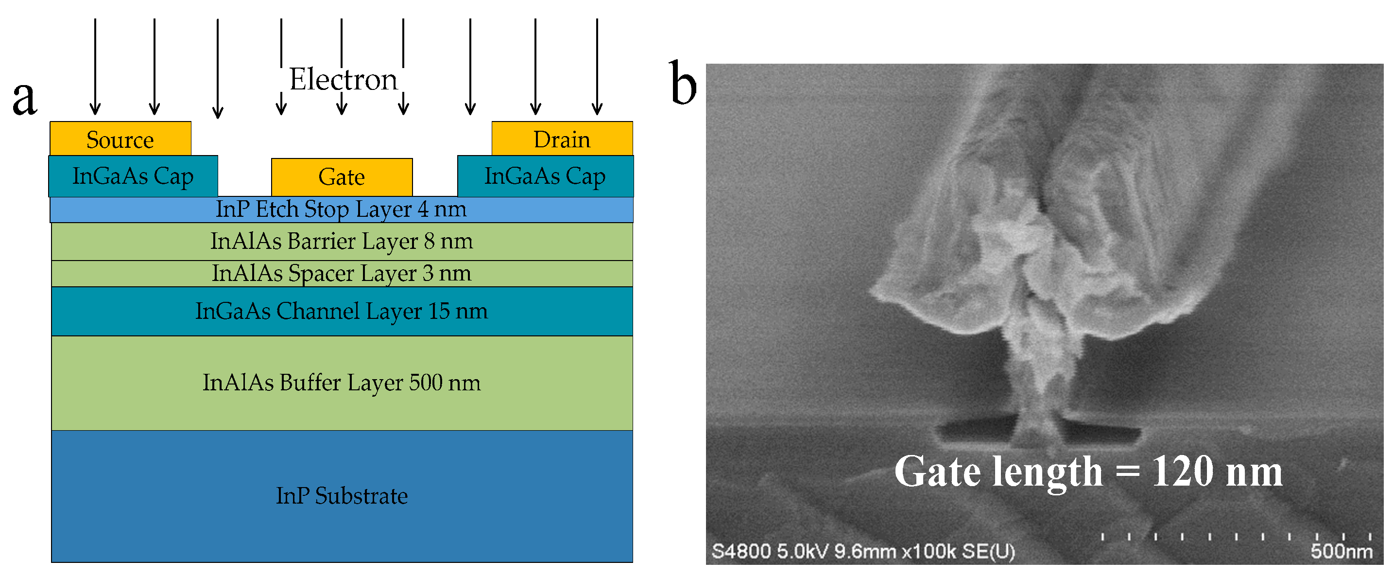
2. Materials and Methods

The InAlAs/InGaAs InP-based HEMTs were developed on a 4-inch compound semiconductor manufacturing assembly line at the Institute of Microelectronics, Chinese Academy of Sciences. The epitaxial structures were successively grown by gas source molecular beam epitaxy (GSMBE) with parameters as shown in Figure 1a. The entire epilayers from bottom to top consisted of an InAlAs buffer, an InGaAs channel, an unstrained InAlAs spacer layer, a Si-doped plane, an lnAlAs Schottky barrier layer, an InP etching stopper layer, and uppermost composite InGaAs cap layers. The composite cap layers were adopted to improve contact characteristics, which contained a highly Si-doped In0.6Ga0.4As cap layer (3 × 1019 cm−2) and a Si-doped In0.53Ga0.47As transition layer (5 × 1018 cm−2). All InAlAs layers were lattice matched with the InP substrate.
The InP-based HEMTs’ fabrication process began with mesa isolation through wet chemical etching based on phosphorus acid, leaving an In0.52Al0.48As buffer layer exposed on the surface. Then, ohmic contacts of source and drain electrodes were formed using non-alloyed Ti/Pt/Au with a 2 μm separation. A 20 nm thick SiO2 was deposited to improve resist adhesion, passivate the device surface, and mechanically support the T-shaped gate. Subsequently, Ti/Au connection wires were formed as coplanar waveguide bond pads. Afterward, 120 nm T-shaped gates were patterned using the EBL technique, and the fine gate-foot pattern was precisely replicated on the SiO2 film. Subsequently, Ti/Pt/Au metallization was carried out and followed by gate-recess etching until the InP etching-stopper layer. Figure 1b depicts a detailed vertical profile of a T-gate by scanning electron microscope (SEM). The detailed fabrication process has also been mentioned elsewhere in [22,23].
InP-based HEMTs with 2 × 50 μm gate width and 120 nm gate length were then irradiated by 1 MeV electrons with fluences of 1 × 1014 cm−2, 1 × 1015 cm−2, and 1 × 1016 cm−2 at room temperature at the Lanzhou Institute of Physics of China. In particular, one quarter of a device wafer from a set of the complete technological process was carved into small pieces for experiments with different fluences, and the average value of three devices was determined for each fluence irradiation to improve precision. The DC and RF characteristics of these devices were measured within 12 h by using a B1500A semiconductor parameter analyzer and N5245A PNA-X vector network analyzer (Keysight Technologies, Made in Malaysia). All the measurements were carried out at room temperature.

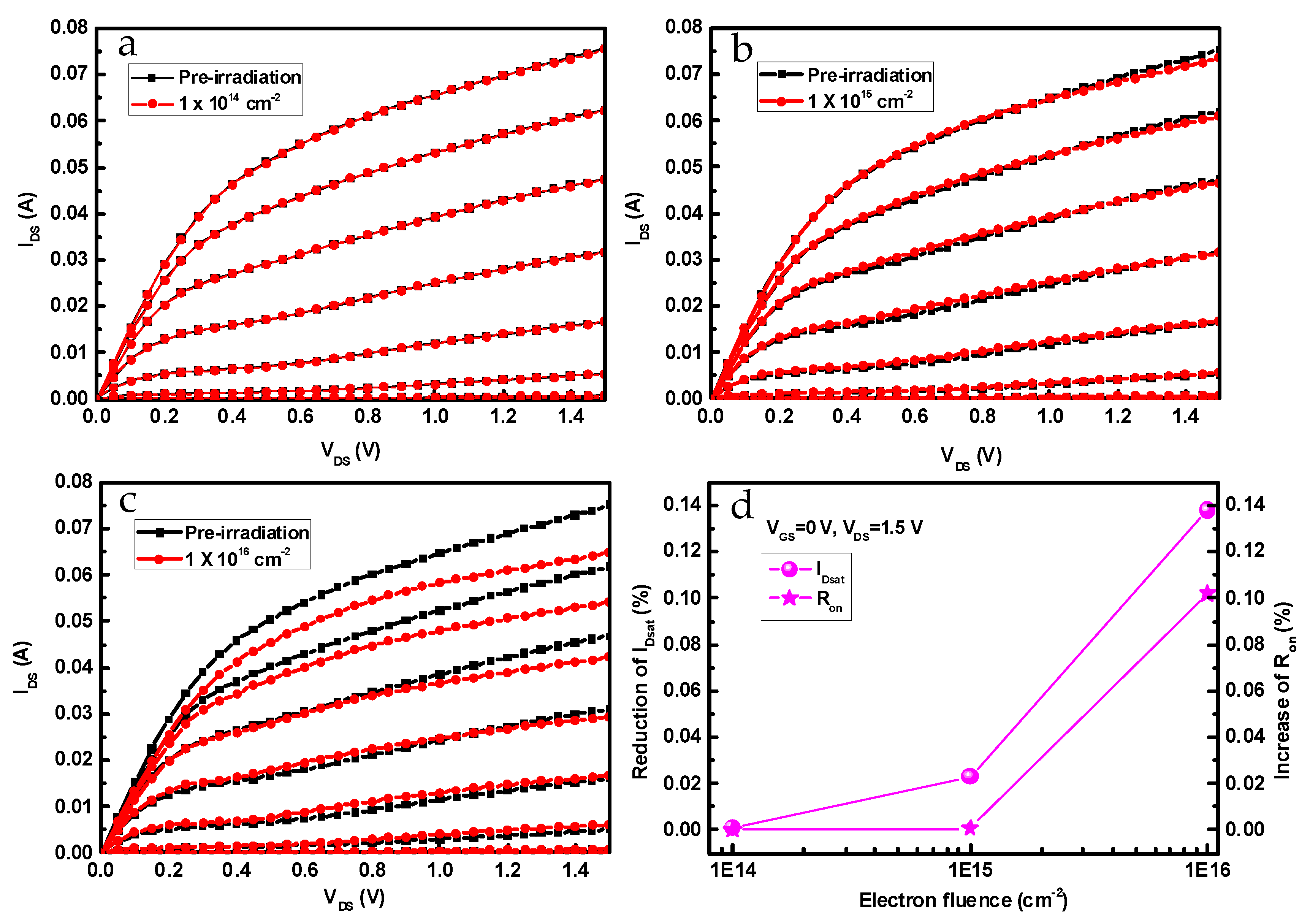
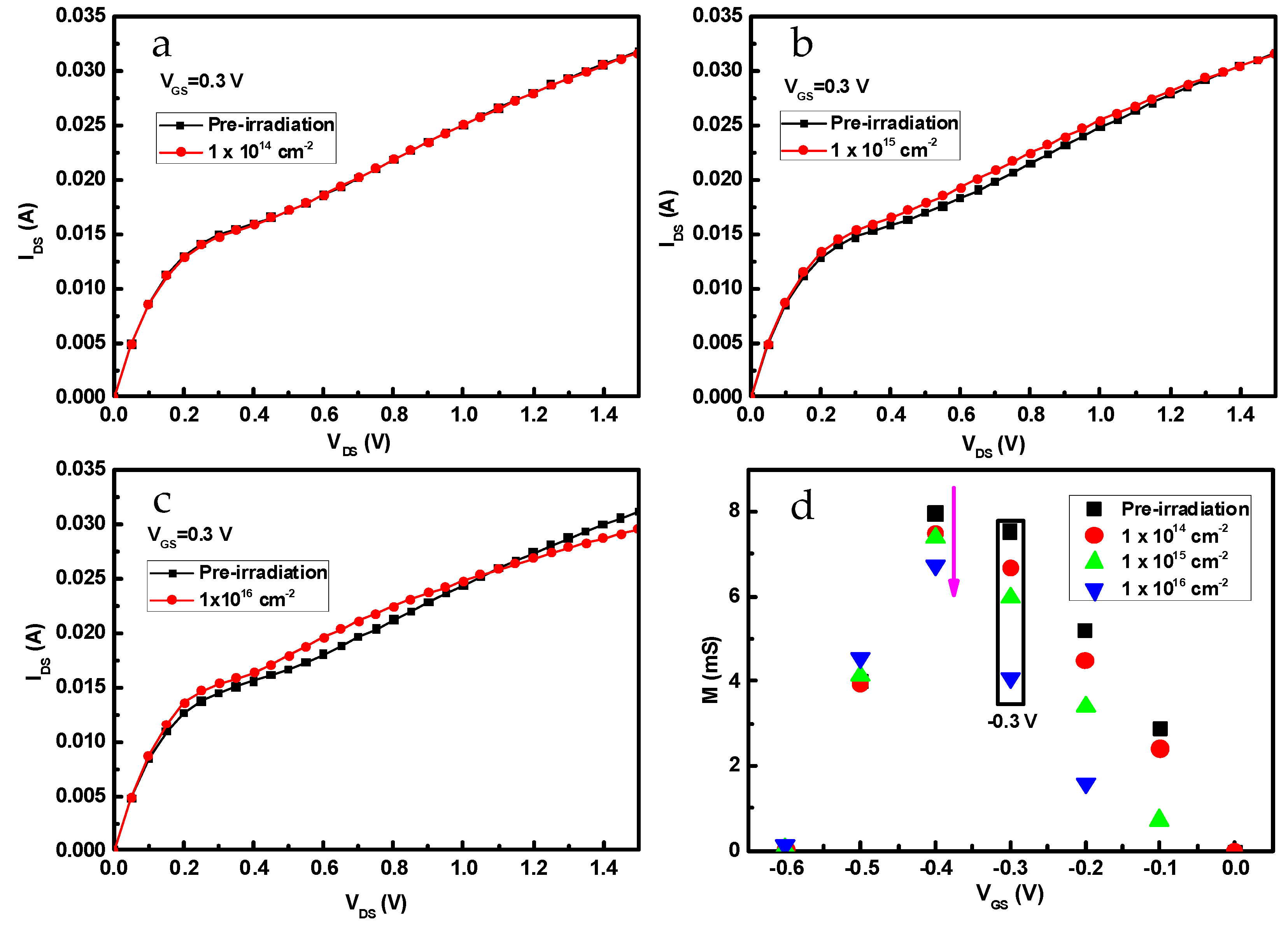
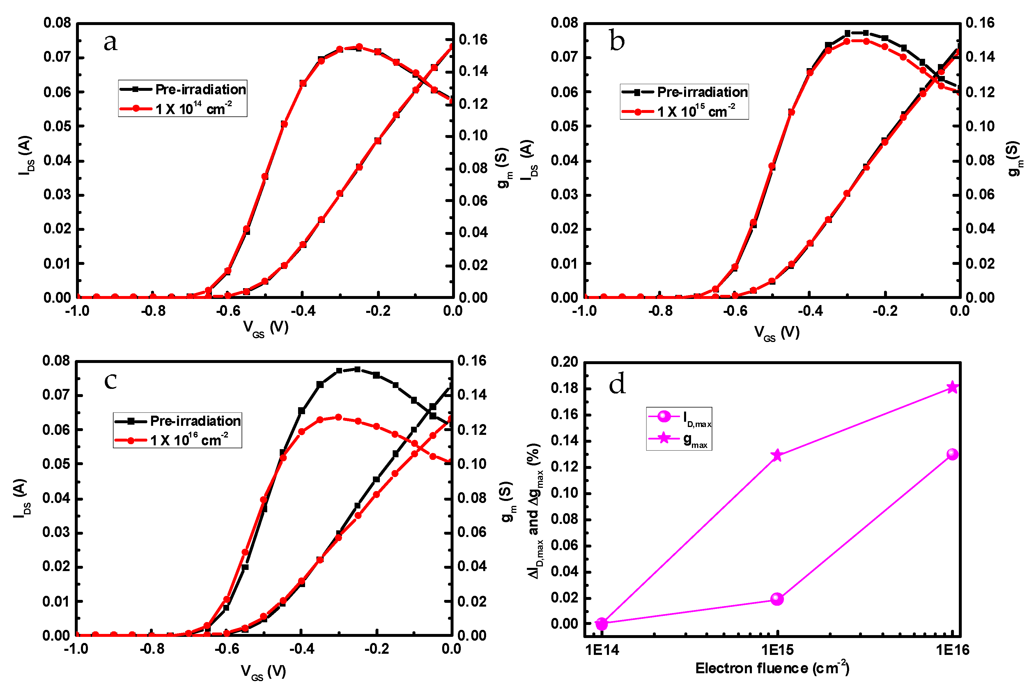
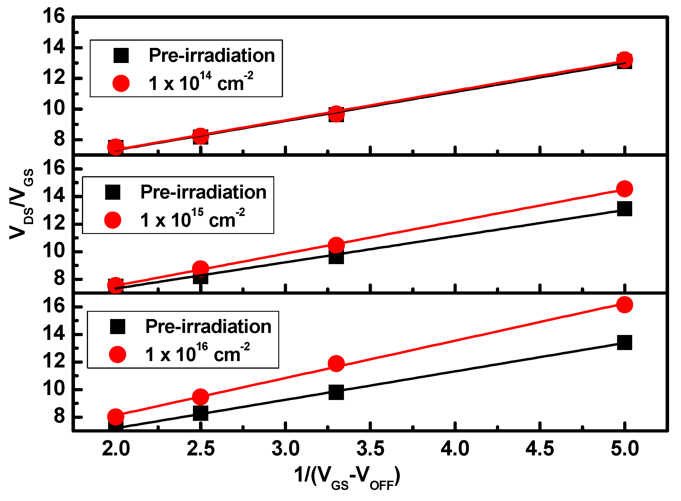
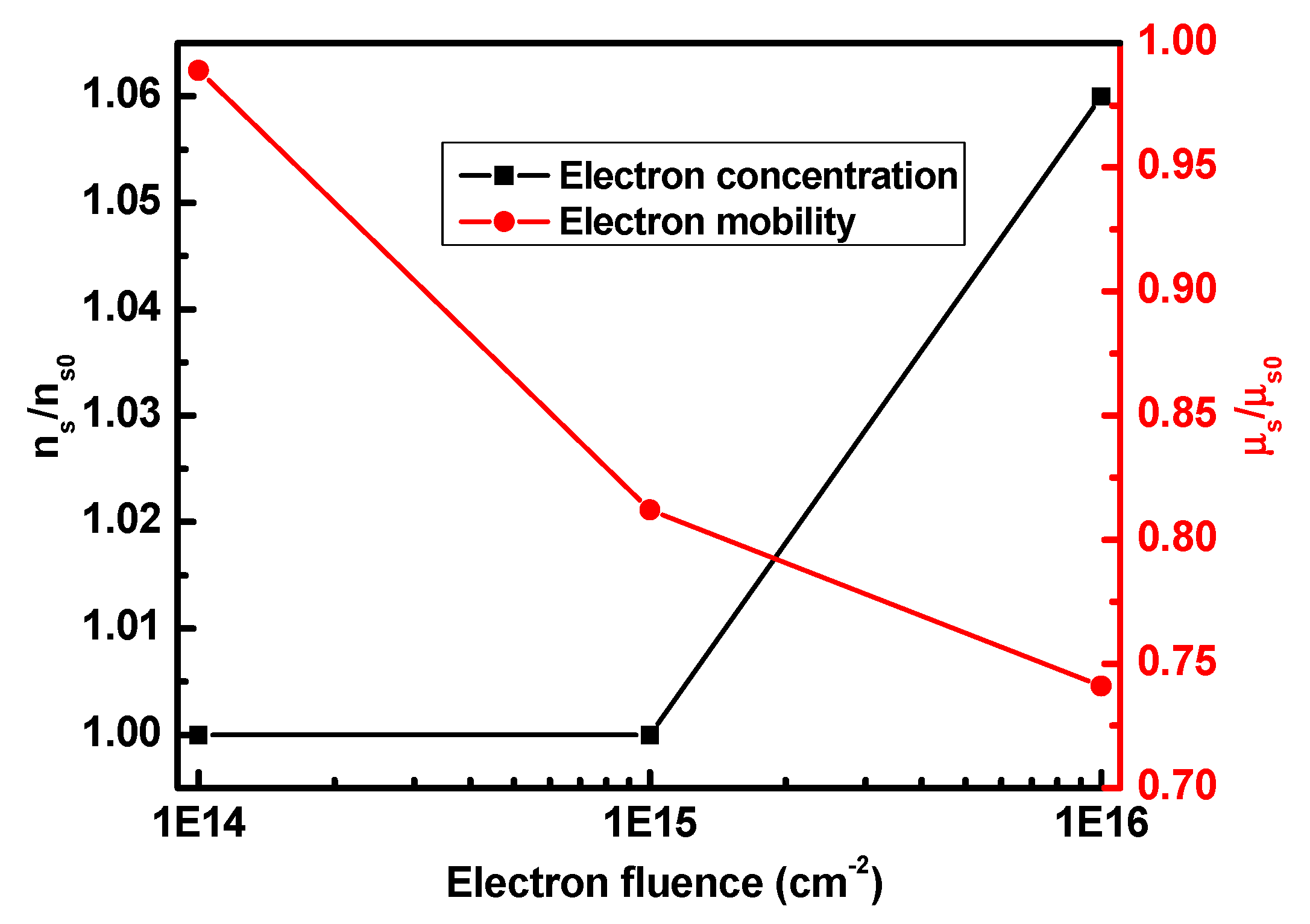
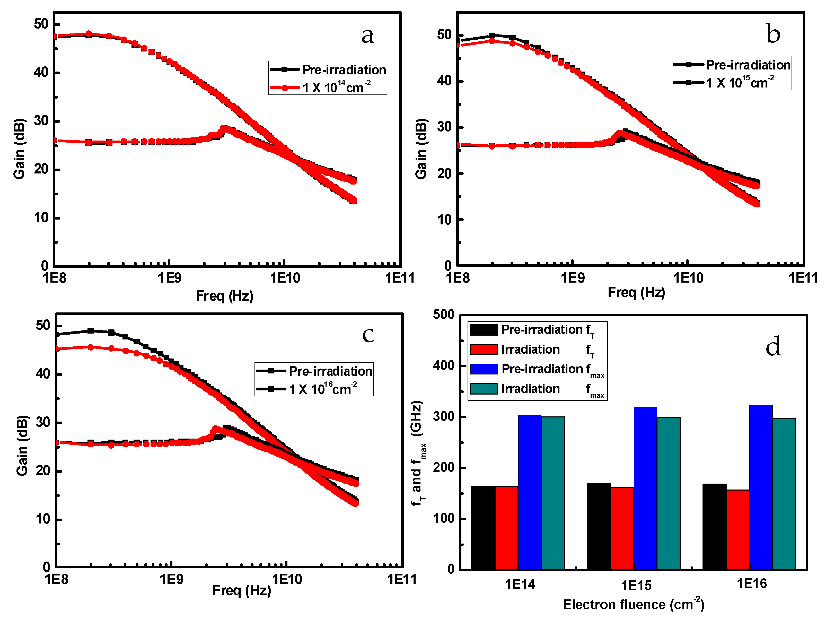
3. Results and Discussion

Figure 2a–c indicates the output characteristics of InP-based HEMTs before and after 1 MeV electron irradiation with fluences of 1 × 1014 cm−2, 1 × 1015 cm−2, and 1 × 1016 cm−2. Gate-source voltage (VGS) varies positively from −0.6 V to 0 V in steps of 0.1 V, whereas drain-source voltage (VDS) sweeps from 0 V to 1.5 V in steps of 0.05 V. It has been found that channel current is nearly unchanged until irradiation fluence reaches 1 × 1015 cm−2; afterward, the channel current (IDS) shows a dramatic drop as irradiation fluence rises. Specifically, saturation channel current (ID,sat) and specific channel on-resistance (Ron) are extracted from the output curves at VGS = 0 V, as shown in Figure 2d. With irradiation fluence increasing to 1 × 1016 cm−2, ID,sat and Ron have deteriorated by 13.8% and 10.2%, respectively. From the output characteristics, the drain-source current was abruptly increased at the lower gate bias, which was the so-called kink effect, as shown in Figure 2. Figure 3 shows the IDS-VDS curve at VDS = −0.3 V. The results indicate that the kink effect was alleviated with the increase of electron fluence, as shown in Figure 3a–c. To understand the variation of the kink effect, the M impact factors with VGS at different electron fluences were calculated, as shown in Figure 3d. With the increase of electron fluence, the M impact factor cuts down and the kink effect becomes weaker. This may be owing to the reduction of the surface states at the gate-recess region after electron irradiation [14].
Figure 4 describes the transfer characteristics of InP-based HEMTs before and after 1 MeV electron irradiation with VDS = 1.4 V. From the transfer curves, the transconductance (gm) and channel current (IDS) were observed to decrease after an irradiation fluence larger than 1 × 1016 cm−2, and the reduction rates (Δ) were computed precisely and are shown in Figure 4d. The maximum transconductance (gm,max) is slumped by 18.1% and the maximum channel current (ID,max) drops down by 12.9% at an electron fluence of 1 × 1016 cm−2.
For HEMT devices, the primary factors which contribute to the change of DC characteristics are the carrier density and mobility in the hetero-junction region. Charged defects in the hetero-junction region are induced by electron irradiation. They may act as compensation centers of majority carriers in the channel region, that is, the carrier removal effect [24]. Meanwhile, the mobility of carriers in the channel changes when their trajectories are affected by irradiation-induced charged defects [25]. To understand the irradiation-induced charged defects on the carrier density and carrier mobility, a charge control model was used, and it can be written as follows [26]:
n s = ε q d ( V GS V O F F ) ,   V DS I DS = R S + R D + L d μ W ε ( V GS V OFF ) ,
where VOFF is the off voltage, RS and RD are the source and drain access resistance, L is the gate length, and W is the gate width. The carrier mobility can be obtained from the slope of the VDS/IDS − 1/(VGSVOFF) curves, as shown in Figure 5. Figure 6 shows the variation of electron concentration and mobility with the electron fluence. The results show that the electron concentration increases slightly and the electron mobility reduces by 25.9% at the electron fluence of 1 × 1016 cm−2. This may be due to the fact that some incident particles may remain in the device structure apart from inducing a reasonable number of defect states [27]. The particles that remained and the induced defects result in the decrease of carrier mobility by scattering. Meanwhile, the incident particles may rearrange the mobile defect states, which lead to some electrons being released from defect sites, and finally the carrier density increases slightly with electron fluence. Therefore, the degeneration of device characteristics are mainly due to the decreasing carrier mobility by electron irradiation.
As a kind of high frequency device, fmax affects the device power gain of the analog circuit, while fT determines the switching speed of the digital circuit. The S-parameters of the InP-based HEMTs irradiated by different fluences were measured over frequencies from 0.1 to 40 GHz with a step size of 0.1 GHz. The parasitic capacitance and inductance induced by pad metals were calibrated and subtracted through open and short pads on the same wafer. The value of fT and fmax can be respectively extrapolated from the current gain (H21) and maximum available/stable power gain (MAG/MSG) using a least squares fitting with a −20 dB/decade slope. The fT and fmax can be written as follows [28]:
f T = g m 2 π ( C gd + C gs )
f max = f T 4 g d ( R S + R i + R G ) + 2 ( C GD / C GS ) [ ( C GD / C GS ) + g m ( R S + R i ) ]
where gd are the out conductance, RG, RS and Ri are the gate, source and channel resistance, respectively, and CGS and CGD are the gate-source capacitance and gate-drain capacitance.
Figure 7 shows the frequency characteristics of InP-based HEMTs before and after 1 MeV electron irradiation with different electron fluences. With the increase of the fluence, both fT and fmax demonstrate a slightly downward trend. From Equations (1) and (2), CGS, CGD, and CGD/CGS are the main factors impacting the fT and fmax of devices. Figure 8a show the variation of CGS and CGD as a function of electron fluence. The results show that the CGD is increasing as the electron fluence rises for the samples. For larger electron fluences, the values of CGD/CGS become larger than before, as shown in the inset of Figure 8a. However, CGS decreases as the electron fluence increases. From Equations (1) and (2), the increase of CGD and CGD/CGS are the main reason for the degradation of the fmax and fT values. In addition, electron irradiation significantly reduces the carrier concentration in the channel and results in an increase of Ron, which may be another important factor for fmax reduction. Figure 8b shows the degradation percentage of fT and fmax in the case of different electron fluences. The fT and fmax are only reduced by 7.1% and 8.2%, respectively, even when the electron fluence rose up to 1 × 1016 cm−2. Therefore, the InP-based HEMT device demonstrates good capability when it works in an irradiation environment.

4. Conclusions

In conclusion, the DC and RF characteristics of InP-based HEMTs were studied before and after 1 MeV electron irradiation. The degradation of DC properties became gradually apparent with the increase of electron fluence, which could attributed to the reduction of carrier mobility in the channel. Furthermore, fT and fmax demonstrated a slightly downward trend. The deterioration of frequency properties was mainly due to the increase of CGD with induced charged traps. Additionally, the specific channel on-resistance Ron increased after electron irradiation, which led to the reduction of fmax. However, the fmax showed a degeneration of only 8.2%, even when the electron fluence rose up to 1 × 1016 cm−2. This shows that an InP-based HEMT device is perfectly suited to work in an irradiation environment.

Author Contributions

Conceptualization, Y.Z. and Z.J.; methodology, S.S. and P.D.; validation, S.S., P.D., Y.Z., and Z.J.; formal analysis, S.S., Y.Z., and Z.J.; investigation, S.S. and Y.L.; resources, Y.Z.; data curation, Z.J., Y.L., and Z.W.; writing—original draft preparation, S.S. and P.D.; writing—review and editing, Y.Z. and Z.J.; visualization, P.D.; supervision, Y.Z., Y.L., and Z.J.; project administration, Y.Z.; funding acquisition, Y.Z., irradiation experiment, Z.W., S.S.; S.S., and P.D. contributed equally to this work.

Funding

This research was funded by the National Natural Science Foundation of China (Nos. 11775191, 61404115, 61434006, 11475256), the Development Fund for Outstanding Young Teachers in Zhengzhou University of China (No. 1521317004), and the Doctoral Student Overseas Study Program of Zhengzhou University, China.

Acknowledgments

The authors would like to express heartfelt thanks to Li Yankui for tuning the measurement equipment. The authors also owe a debt of gratitude to Yuxiong Xue, Lanzhou Institute of Physics of China.

Conflicts of Interest

The authors declare no conflict of interest.

References

  1. Jo, H.B.; Baek, J.M.; Yun, D.Y.; Son, S.W.; Lee, J.H.; Kim, T.W.; Kim, D.H.; Tsutsumi, T.; Sugiyama, H.; Matsuzaki, H. Lg = 87 nm InAlAs/InGaAS high-electron mobility traansistors with a gmax of 3S/mm and fT of 559 GHz. IEEE Electron Device Lett. 2018, 39, 1640–1643. [Google Scholar] [CrossRef]
  2. Baeka, J.M.; Son, S.W.; Park, J.H.; Park, J.K.; Kwak, J.G.; Yoon, J.; Bang, D.S.; Lee, J.H.; Kim, T.; Kim, D.H. Stepper-based Lg = 0.5 μm In0.52Al0.48As/In0.7Ga0.3As PHEMTs on a 3-inch InP substrate with record product of fT and Lg. Solid State Electron. 2018, 147, 58–62. [Google Scholar] [CrossRef]
  3. Zhong, Y.H.; Li, K.K.; Li, X.J.; Jin, Z. A W-band high-gain and low-noise amplifier MMIC using InP-based HEMTs. J. Infrared Millim. Terahertz Waves 2015, 34, 668–672. [Google Scholar]
  4. Li, T.H.; Zheng, G.H.; Liu, C.R.; Xia, W.W.; Li, D.X.; Duan, Z.Y. Analysis of Pressure Distribution in Gas Cushion Press Nanoimprint Lithography. IEEE Trans. Nanotechnol. 2013, 12, 589–595. [Google Scholar]
  5. Shangguan, L.; Ma, L.H.; Li, M.K.; Peng, W.; Zhong, Y.H.; Su, Y.F.; Duan, Z.Y. Study on the shrinkage behavior and conductivity of silver microwires during electrostatic field assisted sintering. J. Phys. D Appl. Phys. 2018, 51, 185603. [Google Scholar] [CrossRef]
  6. Ma, L.H.; Han, W.H.; Zhao, X.S.; Cao, Y.Y.; Dou, Y.M.; Yang, F.H. Influence of dopant concentration on electrical quantum transport behaviors in junctionless nanowire transistors. Chin. Phys. B 2018, 27, 088106. [Google Scholar] [CrossRef]
  7. Ajayan, J.; Ravichandran, T.; Prajoon, P.; Charles Pravin, J.; Nirmal, D. Investigation of breakdown performance in Lg = 20 nm novel asymmetric InP HEMTs for future high-speed high-power applications. J. Comput. Electron. 2018, 17, 265–272. [Google Scholar] [CrossRef]
  8. Mei, X.B.; Yoshida, W.; Lange, M.; Lee, J.; Zhou, J.; Liu, P.H.; Leong, K.; Zamora, A.; Padilla, J.; Sarkozy, S.; et al. First Demonstration of Amplification at 1 THz Using 25-nm InP High Electron Mobility Transistor Process. IEEE Electron Device Lett. 2015, 36, 327–329. [Google Scholar] [CrossRef]
  9. Takahashi, T.; Kawano, Y.; Makiyama, K.; Shiba, S.; Sato, M.; Nakasha, Y.; Hara, N. Enhancement of fmax to 910 GHz by Adopting Asymmetric Gate Recess and Double-Side-Doped Structure in 75-nm-Gate InAlAs/InGaAs HEMTs. IEEE Trans. Electron Device 2017, 64, 89–95. [Google Scholar] [CrossRef]
  10. Yang, G.; Jang, S.; Ren, F.; Pearton, S.J.; Kim, J. Influence of High-Energy Proton Irradiation on β-Ga2O3 Nanobelt Field-Effect Transistors. ACS Appl. Mater. Interfaces 2017, 9, 40471–40476. [Google Scholar] [CrossRef]
  11. Pearton, S.J.; Deist, R.; Ren, F.; Liu, L.; Polyakov, A.Y.; Kim, J. Review of radiation damage in GaN-based materials and devices. J. Vac. Sci. Technol. A 2013, 31, 050801. [Google Scholar] [CrossRef]
  12. Douglas, E.A.; Bielejec, E.; Frenzer, P.; Yates, B.R.; Pearton, S.J.; Lo, C.F.; Liu, L.; Kang, T.S.; Ren, F. Effects of 2 MeV Ge+ irradiation on AlGaN/GaN high electron mobility transistors. J. Vac. Sci. Technol. B 2015, 31, 021205. [Google Scholar] [CrossRef]
  13. Martinez, P.J.; Maset, E.; Gilabert, D.; Kilders, S.E.; Ejea, J.B. Evidence of dynamic-R-on degradation on low-dose Co-60 gamma radiation AlGaN/GaN HEMTs. Semicond. Sci. Technol. 2018, 33, 115017. [Google Scholar] [CrossRef]
  14. Oh, S.K.; Song, C.G.; Jang, T.; Kim, K.C.; Jo, Y.J.; Kwak, J.S. Reduction of Gate Leakage Current on AlGaN/GaN High Electron Mobility Transistors by Electron-Beam Irradiation. J. Nanosci. Nanotechnol. 2013, 13, 1738. [Google Scholar] [CrossRef]
  15. Kimura, T.; Shigemasa, R.; Ohshima, T. Electron irradiation during Schottky gate metal evaporation and its effect on thr stability of InGaAs/A1GaAs HEMTs. Solid State Electron. 1997, 41, 1457. [Google Scholar] [CrossRef]
  16. Gao, F.; Chen, N.; Rivera, E.H.; Huang, D.; LeVan, P.D. Displacement damage and predicted non-ionizing energy loss in GaAs. J. Appl. Phys. 2017, 121, 095104. [Google Scholar] [CrossRef]
  17. Liu, L.; Cuervo, V.C.; Xi, Y.; Ren, F.; Pearton, S.J.; Kim, H.Y.; Kim, J.; Kravchenko, I.I. Impact of proton irradiation on dc performance of AlGaN/GaN high electron mobility transistors. J. Vac. Sci. Technol. B 2013, 31, 042202. [Google Scholar] [CrossRef]
  18. Polyakov, A.Y.; Pearton, S.J.; Frenzer, P.; Ren, F.; Liu, L.; Kim, J. Radiation effects in GaN materials and devices. J. Mater. Chem. C 2013, 1, 877. [Google Scholar] [CrossRef]
  19. Laiadi, W.; Meftah, A.; Sengouga, N.; Meftah, A. Irradiation effect on the electrical characteristics of an AlGaAs/GaAs based solar cell: Comparison between electron and proton irradiation by numerical simulation. Superlattices Microstruct. 2013, 58, 44–52. [Google Scholar] [CrossRef]
  20. Giubileo, F.; Iemmo, L.; Passacantando, M.; Urban, F.; Luongo, G.; Sun, L.; Amato, G.; Enrico, E.; Bartolomeo, A.D. Effect of Electron Irradiation on the Transport and Field Emission Properties of Few-Layer MoS2 Field-Effect Transistors. J. Phys. Chem. C 2019, 123, 1454. [Google Scholar] [CrossRef]
  21. Bartolomeo, A.D.; Pelella, A.; Liu, X.; Miao, F.; Passacantando, M.; Giubileo, F.; Grillo, A.; Iemmo, L.; Urban, F.; Liang, S.J. Pressure-Tunable Ambipolar Conduction and Hysteresis in Thin Palladium Diselenide Field Effect Transistors. Adv. Funct. Mater. 2019, 29, 1902483. [Google Scholar] [CrossRef]
  22. Zhong, Y.H.; Wang, W.B.; Sun, S.X.; Ding, P.; Jin, Z. Long-time thermal stability comparison of alloyed and non-alloyed Ohmic contacts for InP-based HEMTs. Phys. Status Solidi A 2017, 214, 1700411. [Google Scholar] [CrossRef]
  23. Zhong, Y.H.; Yang, J.; Li, X.J.; Ding, P.; Jin, Z. Impact of the silicon-nitride passivation film thickness on the characteristics of InAlAs/InGaAs InP-based HEMTs. J. Korean Phys. Soc. 2015, 66, 1020–1024. [Google Scholar] [CrossRef]
  24. Jun, B.; Subramanian, S. Carrier-removal rate and mobility degradation in heterojunction field-effect transistor structures. IEEE Trans. Nucl. Sci. 2002, 49, 3222. [Google Scholar]
  25. Anderson, T.J.; Koehler, A.D.; Greenlee, J.D.; Weaver, B.D.; Mastro, M.A.; Hite, J.K.; Eddy, C.R.; Kub, F.J.; Hobart, K.D. Substrate-Dependent Effects on the Response of AlGaN/GaN HEMTs to 2-MeV Proton Irradiation. IEEE Electron Device Lett. 2014, 35, 826–828. [Google Scholar] [CrossRef]
  26. Hu, X.W.; Aditya, P.K.; Jun, B.; Daniel, M.F.; Ronald, D.S.; Robert, D.G.; Robert, A.W.; Brad, D.W.; Mykola, B.; Leonard, J.B.; et al. Proton-Irradiation Effects on AlGaN/AlN/GaN High Electron Mobility Transistors. IEEE Trans. Nucl. Sci. 2003, 50, 1791. [Google Scholar]
  27. Lee, I.H.; Lee, C.; Choi, B.; Yun, Y.; Chang, Y.J. Proton-Induced Conductivity Enhancement in AlGaN/GaN HEMT Devices. J. Korean Phys. Soc. 2018, 72, 920. [Google Scholar] [CrossRef]
  28. Tsuyoshi, T.; Yoichi, K.; Kozo, M.; Shoichi, S.; Masaru, S.; Yasuhiro, N.; Naoki, H. Maximum frequency of oscillation of 1.3 THz obtained by using an extended drain-side recess structure in 75-nm-gate InAlAs/InGaAs high-electron-mobility transistors. Appl. Phys. Express 2017, 10, 024102. [Google Scholar]
Figure 1. (a) Epitaxial layer structure of the InP-based high electron mobility transistor (HEMT), (b) scanning electron microscope (SEM) photographs of a vertical profile of the T-gate of InP-based HEMTs.
Nanomaterials 09 00967 g001
Figure 2. Output characteristics of InP-based HEMTs before and after 1 MeV electron irradiation with different irradiation fluences. (a) 1 × 1014 cm−2, (b) 1 × 1015 cm−2, (c) 1 × 1016 cm−2, (d) ID,sat and Ron at VGS = 0 V.
Nanomaterials 09 00967 g002
Figure 3. Output characteristics of InP-based HEMTs before and after 1 MeV electron irradiation with VGS = −0.3 V. (a) 1 × 1014 cm−2, (b) 1 × 1015 cm−2, (c) 1 × 1016 cm−2, (d) M impact factor.
Nanomaterials 09 00967 g003
Figure 4. Transfer characteristics of InP-based HEMTs before and after 1 MeV electron irradiation with different irradiation fluences. (a) 1 × 1014 cm−2, (b) 1 × 1015 cm−2, (c) 1 × 1016 cm−2, (d) Δgm,max and ΔID,max.
Nanomaterials 09 00967 g004
Figure 5. The variation VDS/IDS as a function of 1/(VGSVOFF) for different electron fluences.
Nanomaterials 09 00967 g005
Figure 6. The variation of electron concentration and mobility with the electron fluence.
Nanomaterials 09 00967 g006
Figure 7. Frequency characteristics of InP-based HEMTs before and after 1 MeV electron irradiation with different irradiation fluences. (a) 1 × 1014 cm−2, (b) 1 × 1015 cm−2, (c) 1 × 1016 cm−2, (d) variation of fT and fmax with different electron fluences.
Nanomaterials 09 00967 g007
Figure 8. (a) Dependence of CGS and CGD on electron fluences, (b) degradation percentage of fT and fmax as a function of electron fluence.
Nanomaterials 09 00967 g008

