Article

Effective Modulation of Optical and Photoelectrical Properties of SnS2 Hexagonal Nanoflakes via Zn Incorporation

by
Ganesan Mohan Kumar
1,
Pugazhendi Ilanchezhiyan
1,*,
Hak Dong Cho
2,
Shavkat Yuldashev
1,
Hee Chang Jeon
2,
Deuk Young Kim
3 and
Tae Won Kang
1
1
Nano-Information Technology Academy (NITA), Dongguk University-Seoul, Seoul 04623, Korea
2
Quantum Functional Semiconductor Research Center, Dongguk University-Seoul, Seoul 04623, Korea
3
Division of Physics and Semiconductor Science, Dongguk University-Seoul, Seoul 04623, Korea
*
Author to whom correspondence should be addressed.
Nanomaterials 2019, 9(7), 924; https://doi.org/10.3390/nano9070924
Submission received: 30 May 2019 / Revised: 20 June 2019 / Accepted: 21 June 2019 / Published: 27 June 2019

Abstract

:
Tin sulfides are promising materials in the fields of photoelectronics and photovoltaics because of their appropriate energy bands. However, doping in SnS2 can improve the stability and robustness of this material in potential applications. Herein, we report the synthesis of SnS2 nanoflakes with Zn doping via simple hydrothermal route. The effect of doping Zn was found to display a huge influence in the structural and crystalline order of as synthesized SnS2. Their optical properties attest Zn doping of SnS2 results in reduction of the band gap which benefits strong visible-light absorption. Significantly, enhanced photoresponse was observed with respect to pristine SnS2. Such enhancement could result in improved electronic conductivity and sensitivity due to Zn doping at appropriate concentration. These excellent performances show that Sn1−xZnxS2 nanoflakes could offer huge potential for nanoelectronics and optoelectronics device applications.

1. Introduction

Metal sulfides have received considerable interest due to their unique optoelectronic properties while processed at micro-nano level [1,2,3,4]. In particular, two-dimensional (2D) metal sulfides nanostructures such as nanoplates, nanoflakes and nanosheets have received much attention for their potential application in photodetectors, photovoltaic devices and light-emitting diodes [5,6,7,8,9,10,11,12,13,14,15,16,17,18,19,20]. 2D form of the material offers high specific surface area, making it advantageous for electrochemical, catalytic and photoelectrical activities. Another advantage in 2D materials is that they are more compatible and can easily be integrated into nano-microscale structures for developing new optoelectronic devices [21,22,23,24].
Meanwhile, SnS2 is considered as one of the promising layered materials with excellent visible light absorption and electrical properties. It possesses band gap (2.1–2.3 eV), n-type characteristics, high sensitivity and high surface activity for applications in Li-ion batteries [25], photovoltaic devices [26] and photodetector [27,28]. Variety of nanostructures such as nanoflakes, nanosheets and nanoplates through physical and chemical techniques including chemical vapor deposition, solvothermal and hydrothermal methods have been reported by several groups [29,30]. Among them, nanoflakes preparation via hydrothermal method have attracted considerable interest due to its low cost and large-scale production at low temperatures. Similarly, many efforts have also been made in controlling morphology and enhancing the photoelectrical, chemical and physical properties for improving the device performance. Moreover, dopants in semiconductor could lead to reduction in particle size, narrowing of band gap and enhance the photoelectrical properties of SnS2 [31]. Recently, V and Ti doped SnS2 was reported to be an intermediate band material for application in wider solar absorption [32,33]. Recently doping SnS2 with Fe resulted in room temperature ferromagnetism [34]. Similarly, in our previous work, we reported enhanced optical and electrical properties of SnS2 nanoflakes via Cu doping [35]. More recently, Liu et al. reported enhanced photoresponsivity in Sb doped SnS2 monolayer [36]. Based on the above literatures we test the ability of doping Zn ions in SnS2 to significantly enhance conductivity and sensitivity favorable for its performance in photoelectronics.
The present work reports on hydrothermal synthesis of Zn doped SnS2 nanoflakes at low temperatures. The properties of Sn1−xZnxS2 nanoflakes have been intensively studied through structural, optical and photoelectrical methods. The results show that the Zn doping results in enhanced sensitivity, conductivity and efficiency of charge transfer kinetics. As a proof of concept, Sn1−xZnxS2 nanoflakes were integrated into a patterned indium tin oxide (ITO) substrate (as active material) for photoelectronic device architecture. The results showcased excellent on-off ratio and photoresponse properties than that of pristine counterpart. Our investigations presents Zn doped SnS2 could be a potential candidate for future nano electronic and photoelectronic applications.

2. Experiment

2.1. Synthesis of Sn1−xZnxS2 Nanoflakes

SnS2 and Sn1−xZnxS2 nanoflakes were prepared via low cost hydrothermal route reported previously [35]. In brief, 0.1753 g SnCl4·5H2O (Tin (IV) chloride pentahydrate) and 0.15 g thioacetamide (TAA) were dissolved in 80 mL distilled water, stirred for 1 h to result in homogeneous solution. The prepared solution was transferred to 100 mL Teflon-line autoclave, sealed and heated up to 160 °C for 12 h and finally cooled to room temperature. The prepared SnS2 nanoflakes were then washed with ethanol and deionized water repeatedly and finally dried at 60 °C for 12 h in electric oven. For the synthesis of Sn1−xZnxS2 nanoflakes, 1 and 3 mmol% of Zinc chloride was added to the precursor solution.

2.2. Characterization

The morphological evolution of the sample was examined using field-emission scanning electron microscopy (FESEM, Philips, Model: XL-30, Amsterdam, The Netherland) and field-emission transmission electron microscopy (FE-TEM, JEM-2100F HR, Tokyo, Japan). The phase purity and crystal structure of SnS2 and Sn0.97Zn0.03S2 nanoflakes was inferred through X-ray diffractometer (SmartLab, Rigaku Corporation, Tokyo, Japan). The Raman measurements were performed in a micro-Raman spectrometer (DawoolAttonics, Model: Micro Raman System, Seongnam, Korea) using an excitation wavelength of 532 nm. The chemical composition of Sn0.97Zn0.03S2 was obtained using X-ray photoelectron spectroscopy (K-Alpha+, ThermoFisher Scientific, Waltham, MA, USA). In order to avoid charging effect, during the measurement, charge neutralization was performed with an electron flood gun (K-Alpha+, ThermoFisher Scientific, USA). The absorbance spectrum was recorded using a UV/VIS spectrophotometer (K LAB, Model: Optizen POP, Daejeon, Korea). A Keithley 617 semiconductor parameter analyzer (Tektronix, Beaverton, OR, USA; Model: Keithley 617) was employed to study the photo-response of the device under solar simulator (Newport, OR, USA; AM1.5) (SERIC, Model: XIL-01B50KP).

2.3. Device Fabrication

Initially, 2 mg of samples SnS2 and Sn0.97Zn0.03S2 were added in 10 mL methoxy-ethanol solvent separately and magnetic stirred for 30 min followed by sonication of about 30 min to form colloidal suspension. The resulting suspension was then spin casted on cleaned and patterned ITO/glass substrate at 1000 rpm and dried at 100 °C for 5 min. Several cycles of spin casting process was repeated to obtain a continuous film.

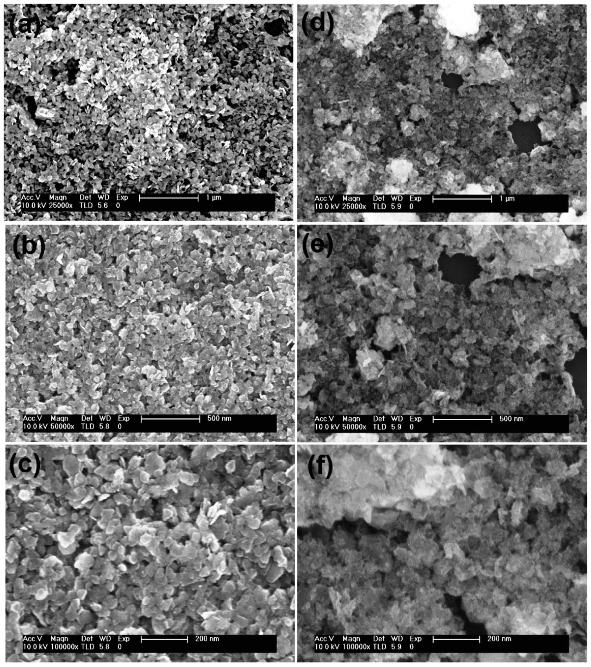
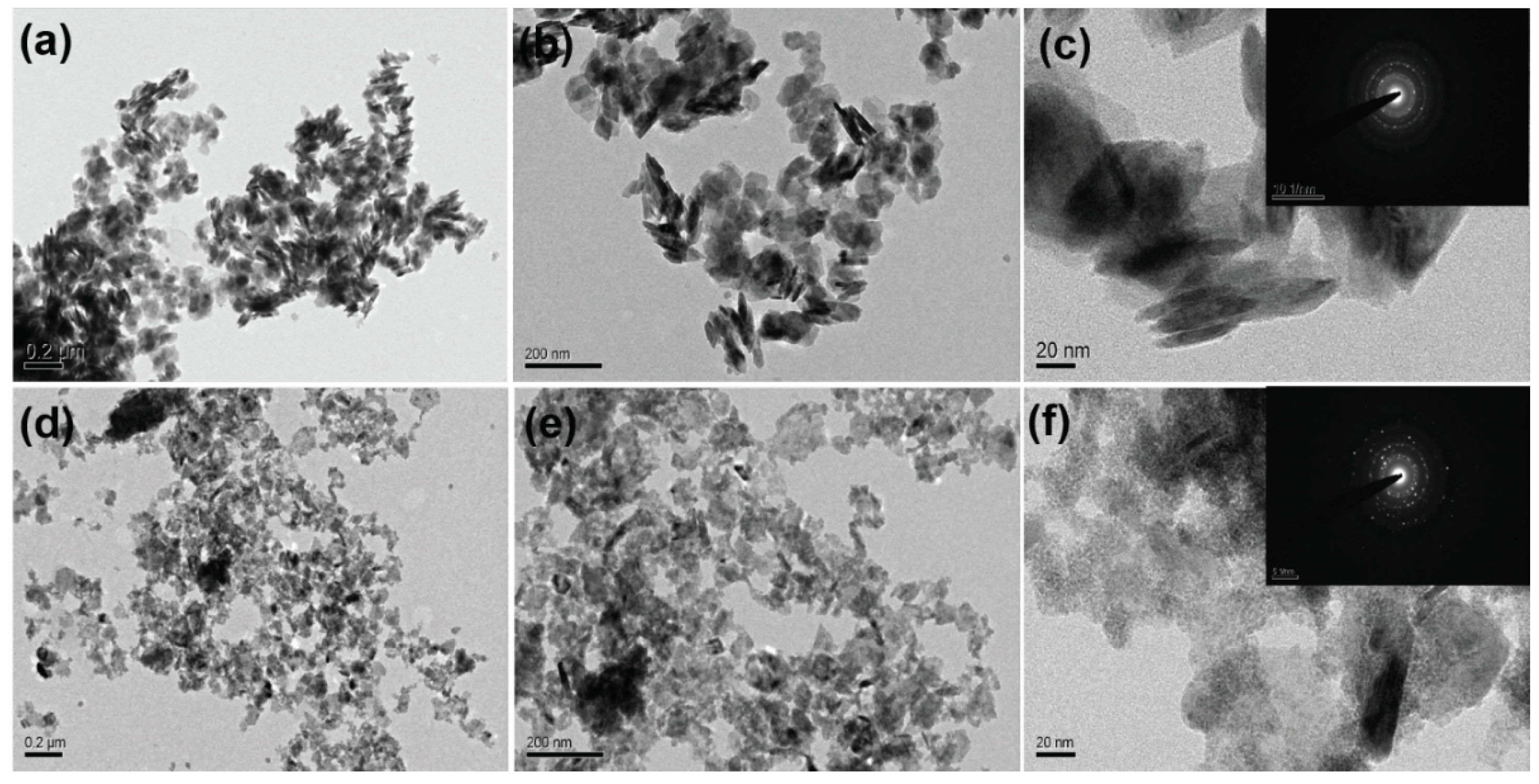
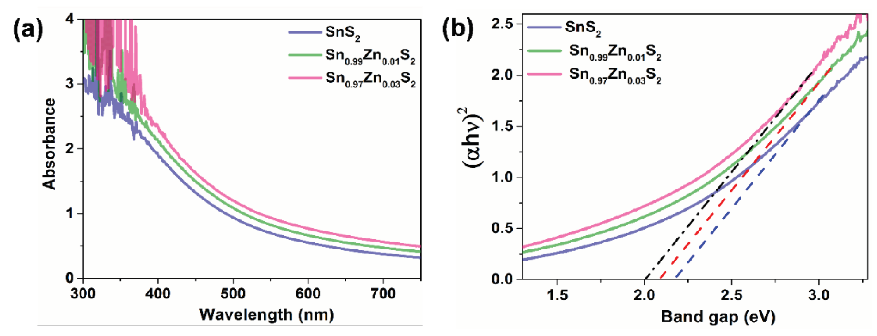
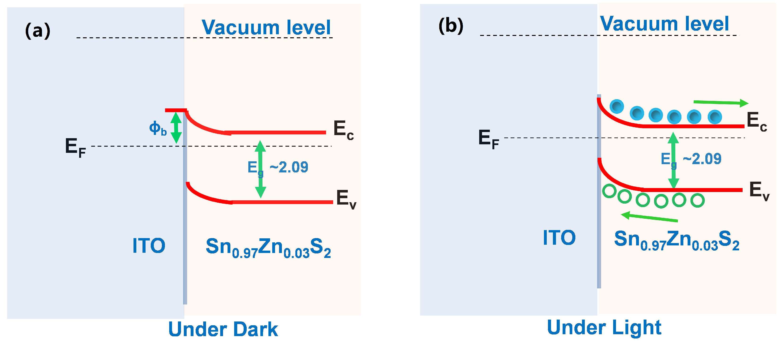
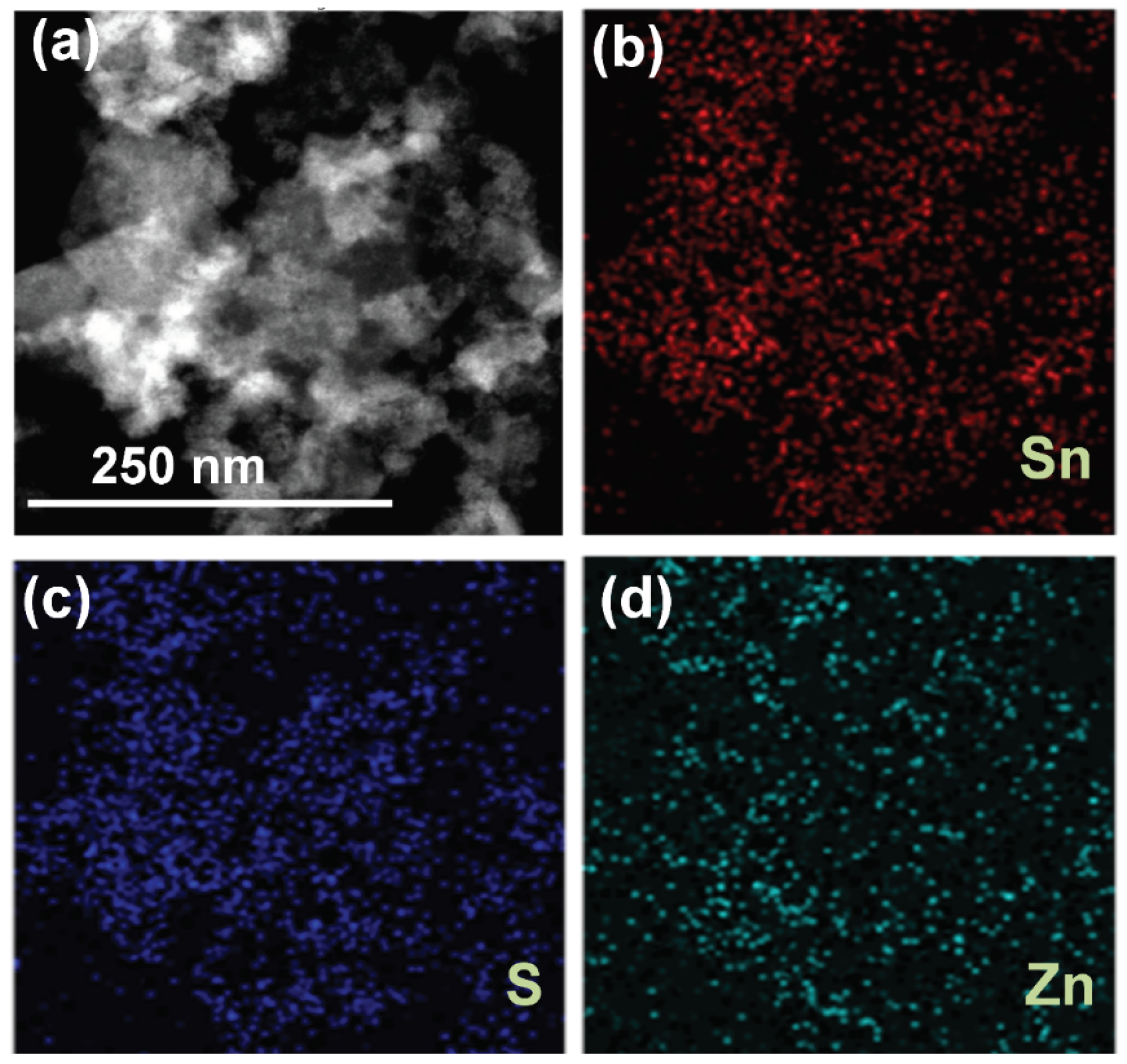
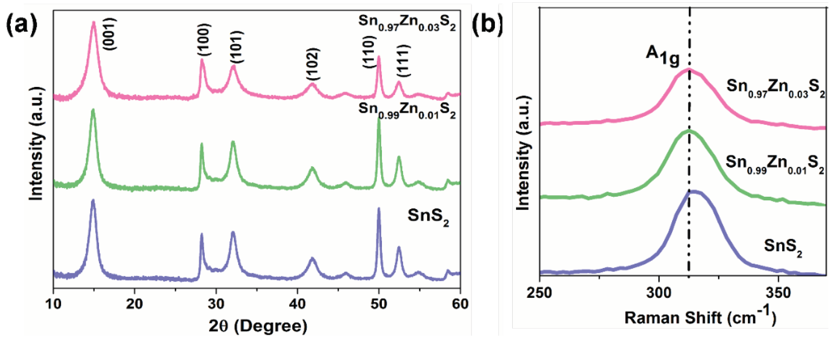
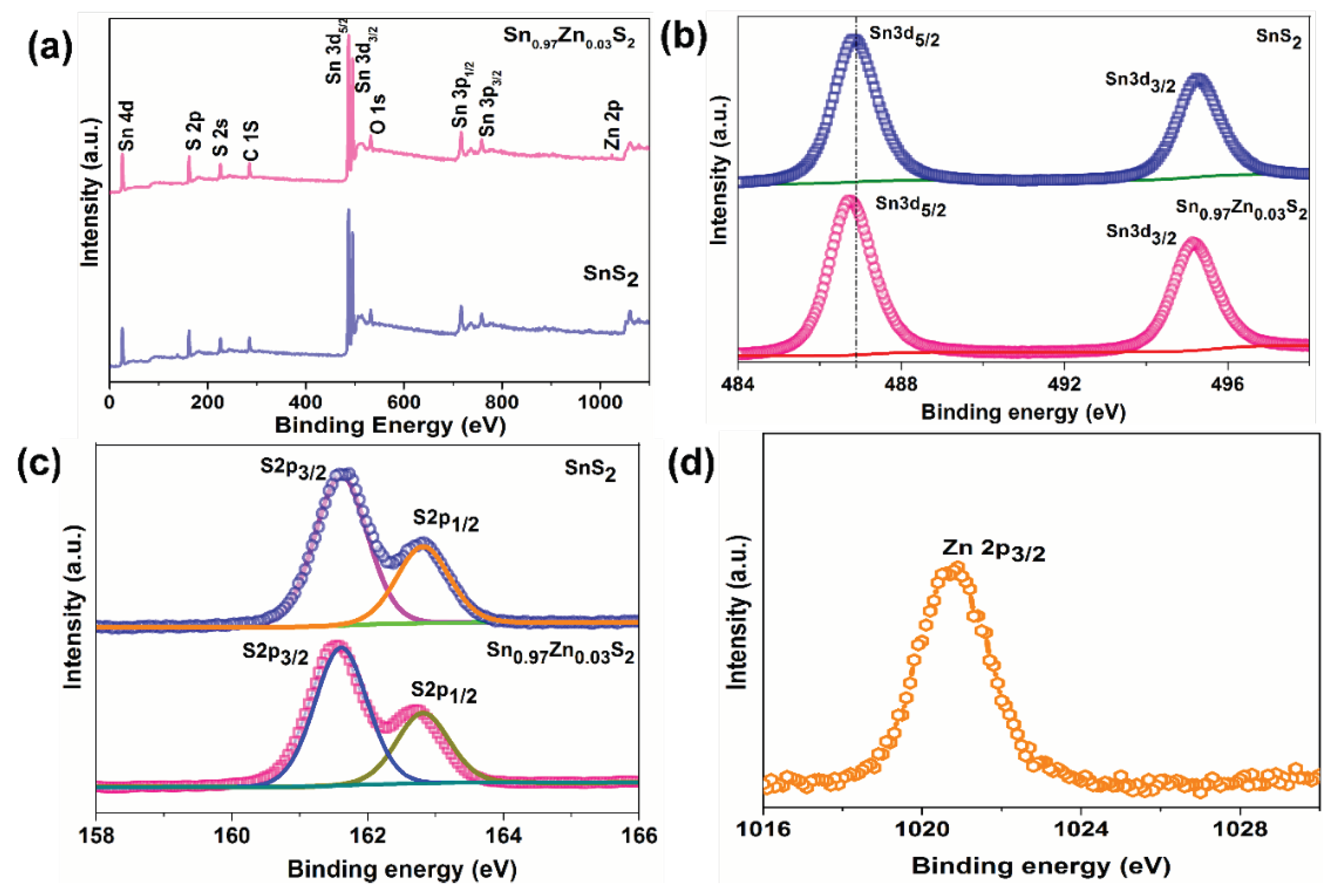
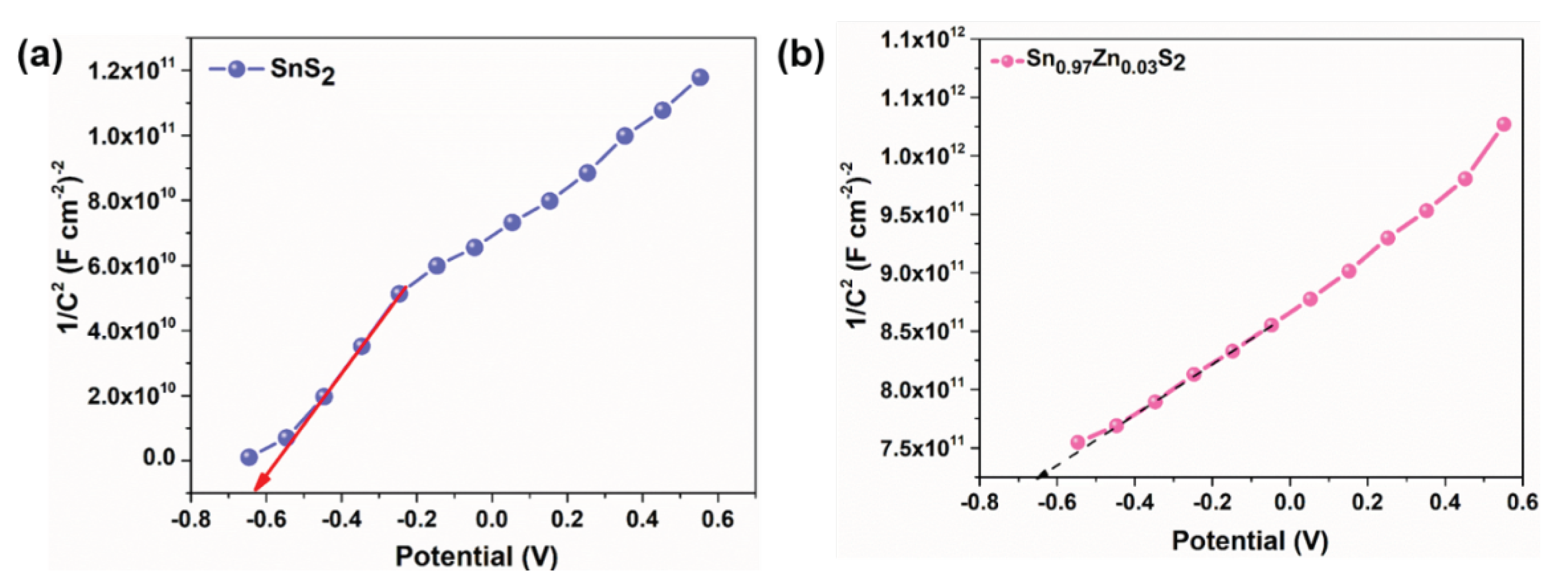
3. Results and Discussions

The morphological features of SnS2, Sn0.99Zn0.01S2 (Figure S1) and Sn0.97Zn0.03S2 products were examined with the aid of field-emission scanning electron microscope (FESEM) technique. The image seen from Figure 1a–c confirms hexagonal nanoflakes with smooth surface and homogeneous distribution in case of pristine SnS2. However, on doping with Zinc the morphology appears to be similar with that of pristine nanoflakes with some random aggregates on the surface of SnS2 (Figure 1d,e). Additionally, transmission electron microscope (TEM) was employed to further investigate the detailed morphological information of SnS2 and Sn0.97Zn0.03S2 products. Figure 2 shows TEM images of pristine SnS2 and Sn0.97Zn0.03S2 nanoflakes with different magnifications. From the Figure 2a–c, it is clear that pristine SnS2 possess typical nanoflakes like structures with hexagonal stacking. Similarly the Sn0.97Zn0.03S2 nanoflakes (Figure 2d–f) also possess indistinguishable hexagonal morphology of pristine SnS2. The inset of Figure 2c,f displays the selected area electron diffraction (SAED) pattern revealing polycrystalline structure of the obtained samples. Energy dispersive spectroscopy (EDS) analysis was further employed in TEM mode to study the homogeneous distribution of Zn element in Sn0.97Zn0.03S2 nanoflakes. Figure 3a–d displays the TEM image and TEM-EDS mapping of Sn0.97Zn0.03S2 nanoflakes. As seen from Figure 3d, Zn element is distributed evenly throughout the whole structure of Sn0.97Zn0.03S2 nanoflakes.
The crystallographic pattern of as synthesized SnS2, Sn0.99Zn0.01S2 and Sn0.97Zn0.03S2 nanoflakes are investigated by XRD analysis and presented in Figure 4a. Here, the strong diffraction peak observed at 2θ = 14.92° belongs to (001) diffraction, is an indication of the hexagonal structure of SnS2 [37]. However, the diffraction peak (001) tends to shift towards smaller angle on Zn doping. This shifting indicates that Zn ions replace Sn sites in the SnS2 crystal matrix. Furthermore, no peaks related to other compounds namely, ZnS and ZnSnS3 are observed in the XRD pattern. Additionally, Raman measurement was further analyzed to study detailed information about the structural properties of Zn doped SnS2 nanoflakes. Raman spectrum for sample SnS2, Sn0.99Zn0.01S2 and Sn0.97Zn0.03S2 nanoflakes are displayed in Figure 4b. Here, in case of pristine SnS2, Sn0.99Zn0.01S2 and Sn0.97Zn0.03S2 nanoflakes, a strong signal was observed at 312 cm−1, which is related to A1g phonon vibration mode of SnS2 [38,39,40].
To elucidate the chemical composition of pristine and Sn0.97Zn0.03S2 nanoflakes, XPS measurements have been carried out and shown in Figure 5a. XPS full survey spectrum (Figure 5a) confirms the presence of Zn doping in SnS2. Figure 5b,c displays the XPS spectra of Sn 3d and S 2p peaks for Sn0.97Zn0.03S2 nanoflakes. As observed in Figure 5b,c, the peaks of Sn 3d at 486.33 and 494.4 eV of Sn 3d is ascribed to Sn3d3/2 and Sn3d5/2 and peaks at 161.2 and 163.3 eV correspond to S 2p peaks of SnS2. These results are consistent with those reported for SnS2 [41,42]. The binding energies of Sn 3d5/2 peak corresponding to pristine SnS2 was observed at 486.47 eV. Subsequently doping with Zn on SnS2, peaks of Sn 3d5/2 shifts to lower energy position to 486.33 eV. The shifting in the binding energy value of Sn 3d5/2 peak was about 0.14 eV compared to pristine SnS2. This shift might be due to Zn ion replace Sn sites in the SnS2 crystal lattice. Figure 5d shows the XPS spectrum for Zn in SnS2 nanoflakes. Besides, the Zn 2p3/2 peak appeared at 1021.3 eV is attributed to Zn2+ bonding state [43], confirming Zn2+ ions have been incorporated into the SnS2.
Figure 6a shows UV–visible absorption spectrum of SnS2, Sn0.99Zn0.01S2 and Sn0.97Zn0.03S2 in the range of 300–750 nm. SnS2 displays a strong absorption in visible part of the solar spectrum. However, in contrast the samples Sn0.99Zn0.01S2 and Sn0.97Zn0.03S2 displayed a broad light absorption in 300 to 750 nm, which indicates that doping Zn ion can result in extending of absorption edge of SnS2. This results suggests that samples Sn0.97Zn0.03S2 possess greater potential than that of pristine sample SnS2 to drive photo excited charge carriers under the light irradiation. The values estimated was found to be 2.24 eV for sample SnS2 which is consistent with our previous result (Figure 6b). However, the values was found to be 2.19 and 2.09 eV for sample Sn0.99Zn0.01S2 and Sn0.97Zn0.03S2. It shows band gap becomes narrower than pristine SnS2 as the Zn content increases [44,45]. This reduction in the band gap might be due to modification in the electronic structures of SnS2 due to Zn doping, which results in creating energy levels in the band gap. This band gap could result in better absorption in visible region and can increase photo excited charge carriers under illumination.
Mott–Schottky (M–S) analysis was made to study the electrical properties of pristine SnS2, Sn0.99Zn0.01S2 and Sn0.97Zn0.03S2 nanoflakes. Generally, Mott–Schottky plot was employed to determine the donor density (Nd) and flat band potential (Vfb) of the materials. M–S analysis are generally expressed by [46,47,48]
1/C2 = (2/eεεoNd)[(VfbV) − kBT/e]
where e is the electronic charge, ε is the dielectric constant of SnS2, ε0 is the relative permittivity, Nd dopant density, V the applied potential, C the specific capacitance, kB the Boltzmann constant and Vfb the flat band potential. The M–S plots of pristine SnS2, Sn0.99Zn0.01S2 (Figure S2) and Sn0.97Zn0.03S2 nanoflakes are displayed in Figure 7. Here Vfb was determined from intercept between the extrapolated linear plot of the curve and was estimated to be ~0.67 V for pristine SnS2 and 0.64 V for Sn0.97Zn0.03S2 nanoflakes. Additionally the difference in the slope reflects the variation in the carrier density (Nd). The values of carrier density was estimated from the Equation (1) to be about 1.46 × 10¹⁹ and 0.47 × 10¹⁹ and in case of SnS2 and Sn0.97Zn0.03S2 nanoflakes.
A photoelectronic device was constructed on samples SnS2 and Sn0.97Zn0.03S2 to study its potential for optoelectronics applications (Figure 8a), (for the details of fabrication process refer Expt. sections). I-V curves of pristine SnS2 nanoflakes at various illumination intensities and dark condition is displayed in Figure 8b. Inset shows I-V curves of the pristine SnS2 nanoflakes under dark and illumination. Here, the I-V curve shows a roughly symmetric behavior indicating Schottky-like junction established at ITO and SnS2 contacts. The dark current was noted to be 0.29 μA at a bias of 3 V. In contrast, the enhancement of current was measured and the value reaches to 0.98 μA under illumination, demonstrating excellent photosensitivity of the SnS2 samples. I-V curves of Sn0.97Zn0.03S2 nanoflakes device under illumination and dark is displayed in Figure 8c. Here, the value of dark current was found to increase than that of pristine SnS2, which suggests reduction in resistance of SnS2 after Zn doping. However, a notable enhancement in photocurrent under illumination was noted compared to that of dark current at same bias voltage in Sn0.97Zn0.03S2 nanoflakes device, indicating their excellent sensitivity. Moreover, photo to dark current (Ilight/Idark) ratio for Sn0.97Zn0.03S2 device (~10.1) tends to increase compared to pristine SnS2 (~3.37). The high sensitivity and enhancement in photocurrent of Sn0.97Zn0.03S2 nanoflakes reveal the effective separation of photoexcited carriers in samples, which are actually promoted after Zn-doping. Figure 8d shows I-V curves of the Sn0.97Zn0.03S2 device measured at room temperature under different light intensities. The photocurrent increases with increasing light intensities revealing strong and clear photon-induced currents phenomena, indicating excellent photoresponse ability of the device. Under illumination, photoexcited charge carriers are mainly generated in Sn0.97Zn0.03S2. Then the charge carriers are quickly separated and driven towards the nearby electrodes due to built-in electric field created at the interface, resulting in photocurrent generation.
Figure 9a shows light intensity-dependent photocurrent values of pristine SnS2 and Sn0.97Zn0.03S2 device. The observed photocurrent value to illumination intensities suggest that the charge carrier photo-generation efficiency is proportional to the number of photons absorbed by the pristine SnS2 and Sn0.97Zn0.03S2 nanoflakes. Reliable response speed and stability to illumination conditions are crucial for the photoelectronic device. To address this concern, time related photoresponse of pristine SnS2 and Sn0.97Zn0.03S2 device was measured with turning light on/off condition for a period of 10 seconds for multiple cycles. Figure 9b,c shows time related photoresponse of the pristine and Sn0.97Zn0.03S2 device under several switch on and switch off conditions. Here, the photocurrent of pristine SnS2 was found to be 0.8 µA. Interestingly the photocurrent is improved by two fold in case of Sn0.97Zn0.03S2 nanoflakes (1.75 µA) compared to pristine SnS2 (Figure 9c). The photoresponse enhancement could be related to Zn ions which acts as an effective dopant and enhance charge separation taking place at the interface. The rise/decay time was measured to be 0.2 and 0.2 s. The reason for the relative longer response speed in our case is probably related to the formation of interface states between the Sn0.97Zn0.03S2 nanoflakes and ITO substrate, which can block the photo-generated carriers, resulting in long life time of the photo-generated carriers. Meanwhile, the device shows no fluctuation under illumination for several repetitive cycles, inferring the excellent stability of the Sn0.97Zn0.03S2 device. The time related response of the Sn0.97Zn0.03S2 device under varied light intensities are displayed in Figure 9d. Here, the photocurrent value varies with different light intensities demonstrating excellent reproducibility of Sn0.97Zn0.03S2 based device. Such high and stable photoresponse behavior may come from the fact that Zn ions act as an effective dopant and result in increased light absorption, which enhances photogenerated charge carriers and leads to an enhanced photocurrent of the device. Thus, photoelectrical studies on Sn0.97Zn0.03S2 nanoflakes illustrates that Zn doping in SnS2 results in significant enhancement of their optoelectronic properties, which leads to improved conductivity and sensitivity.
The mechanism involved in the enhanced photoresponse of Sn0.97Zn0.03S2/ITO structure was explained through energy band diagram in Figure 10. Since the work function between ITO and Sn0.97Zn0.03S2 is different, a Schottky-type behavior is established at Sn0.97Zn0.03S2/ITO interface (Figure 10). Due to this behavior, an electric field was established at the Sn0.97Zn0.03S2/ITO interface. This electric field then accelerates the separation of the photoexcited charge carriers without the application of any applied bias. When illuminated, photoexcited charge carriers produced in Sn0.97Zn0.03S2 are then separated at the Sn0.97Zn0.03S2/ITO interface. This charge carriers separation which was induced due to the electric field results in band bending at the Sn0.97Zn0.03S2/ITO interface. As a result, the photoexcited charge carriers are swept towards ITO electrodes, involving in enhancement of photocurrent (Figure 10b).

4. Conclusions

In summary, Sn0.97Zn0.03S2 nanoflakes were prepared via low temperature hydrothermal synthesis. The modulation of the structural and photoelectrical properties in SnS2 via doping Zinc have been discussed in detail. A shift in XPS peak of Sn 3d5/2 and S 2p3/2 has been observed in Sn0.97Zn0.03S2 nanoflakes due to Zn ion replaced Sn sites in the SnS2 crystal lattice. Optical properties studies show that Sn0.97Zn0.03S2 nanoflakes possess higher visible-light absorption than that of pristine SnS2. Photoelectrical properties based on Sn0.97Zn0.03S2 nanoflakes reveal that Zn doping leads to significant improvement in conductivity and sensitivity to illuminations compared to pristine SnS2. Such an excellent performance of Sn0.97Zn0.03S2 nanoflakes may endow it as a potential candidate for emerging 2D materials in optoelectronic applications.

Supplementary Materials

The following are available online at https://www.mdpi.com/2079-4991/9/7/924/s1, Figure S1: SEM image of Sn0.99Zn0.01S2 nanoflakes, Figure S2: Mott–Schottky plot of Sn0.99Zn0.01S2 nanoflakes.

Author Contributions

Conceptualization: G.M.K. and P.I.; data curation, G.M.K., H.D.C., H.C.J. and P.I.; supervision, T.W.K.; validation, G.M.K. and S.Y.; visualization, T.W.K. and D.Y.K.; writing—original draft, P.I.; all authors read and approved the final manuscript.

Acknowledgements

This work was supported by the Basic Science Research Program through the National Research Foundation of Korea (NRF) grant funded by the Ministry of Education (no. 2018R1D1A1B07051461, no. 2018R1D1A1B07051474, no. 2018R1D1A1B07051406, no. 2018R1D1A1B07050237, no. 2018R1D1A1B07051095, no. 2017R1D1A1B03032759 and no. 2016R1A6A1A1A01012877).

Conflicts of Interest

The authors declare no conflict of interest.

References

  1. Wang, Q.H.; Kalantar-Zadeh, K.; Kis, A.; Coleman, J.N.; Strano, M.S. Electronics and optoelectronics of two-dimensional transition metal dichalcogenides. Nat. Nanotechnol. 2012, 7, 699–712. [Google Scholar] [CrossRef] [PubMed]
  2. Najmaei, S.; Liu, Z.; Zhou, W.; Zou, X.; Shi, G.; Lei, S.; Yakobson, B.I.; Idrobo, J.; Ajayan, P.M.; Lou, J. Vapour phase growth and grain boundary structure of molybdenum disulphide atomic layers. Nat. Mater. 2013, 12, 754–759. [Google Scholar] [CrossRef] [PubMed]
  3. Chhowalla, M.; Shin, H.S.; Eda, G.; Li, L.-J.; Loh, K.P.; Zhang, H. The Chemistry of two- dimensional layered transition metal dichalcogenides nanoflakes. Nat. Chem. 2013, 5, 263–275. [Google Scholar] [CrossRef] [PubMed]
  4. Van der Zande, A.M.; Huang, P.Y.; Chenet, D.A.; Berkelbach, T.C.; You, Y.; Lee, G.-H.; Heinz, T.F.; Reichman, D.R.; Muller, D.A.; Hone, J.C. Grains and grain boundaries in highly crystalline monolayer molybdenum disulphide. Nat. Mater. 2013, 15, 554–561. [Google Scholar] [CrossRef] [PubMed]
  5. Cheng, L.; Huang, W.; Gong, Q.; Liu, C.; Liu, Z.; Li, Y.; Dai, H. Ultrathin WS2 nanoflakes as a high-performance electrocatalyst for the hydrogen evolution reaction. Angew. Chem. Int. Ed. 2014, 53, 7860–7863. [Google Scholar] [CrossRef] [PubMed]
  6. Peimyoo, N.; Yang, W.; Shang, J.; Shen, X.; Wang, Y.; Yu, T. Chemically driven tunable light emission of charged and neutral excitons in monolayer WS2. ACS Nano 2014, 8, 11320–11329. [Google Scholar] [CrossRef] [PubMed]
  7. Late, D.J.; Liu, B.; Ramakrishna Matte, H.S.S.; Dravid, V.P.; Rao, C.N.R. Hysteresis in single-layer MoS2 field effect transistors. ACS Nano 2012, 6, 5635–5641. [Google Scholar] [CrossRef] [PubMed]
  8. Wang, H.; Yuan, H.; Hong, S.S.; Li, Y.; Cui, Y. Physical and chemical tuning of two-dimensional transition metal dichalcogenides. Chem. Soc. Rev. 2015, 44, 2664–2680. [Google Scholar] [CrossRef] [PubMed]
  9. Sun, Y.; Sun, Z.; Gao, S.; Cheng, H.; Liu, Q.; Piao, J.; Yao, T.; Wu, C.; Hu, S.; Wei, S.; et al. Fabrication of flexible and freestanding zinc chalcogenide single layers. Nat. Commun. 2012, 3, 1057–1063. [Google Scholar] [CrossRef]
  10. Lei, F.; Sun, Y.; Liu, K.; Gao, S.; Liang, L.; Pan, B.; Xie, Y. Oxygen vacancies confined in ultrathin indium oxide porous sheets for promoted visible-light water splitting. J. Am. Chem. Soc. 2014, 136, 6826–6829. [Google Scholar] [CrossRef]
  11. Yang, J.; Son, J.S.; Yu, J.H.; Joo, J.; Hyeon, T. Advances in the colloidal synthesis of two-dimensional semiconductor nanoribbons. Chem. Mater. 2013, 25, 1190–1198. [Google Scholar] [CrossRef]
  12. Huang, J.-K.; Pu, J.; Hsu, C.-L.; Chiu, M.-H.; Juang, Z.-Y.; Chang, Y.-H.; Chang, W.-H.; Iwasa, Y.; Takenobu, T.; Li, L.-J. Large area synthesis of highly crystalline WSe2 monolayers and device applications. ACS Nano 2014, 8, 923–930. [Google Scholar] [CrossRef] [PubMed]
  13. Zeng, Z.; Yin, Z.; Huang, X.; Li, H.; He, Q.; Lu, G.; Boey, F.; Zhang, H. Single-layer semiconducting nanoflakes: High-yield preparation and device fabrication. Angew. Chem. Int. Ed. 2011, 50, 11093–11097. [Google Scholar] [CrossRef]
  14. Xia, J.; Zhu, D.; Wang, L.; Huang, B.; Huang, X.; Meng, X.-M. Large-scale growth of two-dimensional SnS2 crystals driven by screw dislocations and application to photodetectors. Adv. Funct. Mater. 2015, 25, 4255–4261. [Google Scholar] [CrossRef]
  15. Fu, X.; Ilanchezhiyan, P.; Mohan Kumar, G.; Cho, H.D.; Zhang, L.; Sattar Chan, A.; Lee, D.J.; Panin, G.N.; Kang, T.W. Tunable UV-visible absorption of SnS2 layered quantum dots produced by liquid phase exfoliation. Nanoscale 2017, 9, 1820–1826. [Google Scholar] [CrossRef] [PubMed]
  16. Tao, Y.; Wu, X.; Wang, W.; Wang, J. Flexible photodetector from ultraviolet to near infrared based on a SnS2 nanosheet microsphere film. J. Mater. Chem. C 2015, 3, 1347–1353. [Google Scholar] [CrossRef]
  17. Huang, Y.; Deng, H.-X.; Xu, K.; Wang, Z.-X.; Wang, Q.-S.; Wang, F.-M.; Wang, F.; Zhan, X.-Y.; Li, S.-S.; Luo, J.-W.; et al. Highly sensitive and fast phototransistor based on large size CVD-grown SnS2 nanoflakes. Nanoscale 2015, 7, 14093–14099. [Google Scholar] [CrossRef]
  18. Mohan Kumar, G.; Fu, X.; Ilanchezhiyan, P.; Yuldashev, S.U.; Lee, D.J.; Cho, H.D.; Kang, T.W. Highly sensitive flexible photodetectors based on self-assembled tin monosulfide nanoflakes with graphene electrodes. ACS Appl. Mater. Interfaces 2017, 9, 32142–32150. [Google Scholar] [CrossRef]
  19. Mohan Kumar, G.; Xiao, F.; Ilanchezhiyan, P.; Yuldashev, S.U.; Kang, T.W. Enhanced photoelectrical performance of chemically processed SnS2 nanoplates. RSC Adv. 2016, 6, 99631–99637. [Google Scholar] [CrossRef]
  20. De, D.; Manongdo, J.; See, S.; Zhang, V.; Guloy, A.; Peng, H.B. High on/off ratio field effect transistors based on exfoliated crystalline SnS2 nano-membrane. Nanotechnology 2013, 24, 025202. [Google Scholar] [CrossRef]
  21. Ye, X.; Chen, J.; Engel, M.; Millan, J.A.; Li, W.; Qi, L.; Xing, G.; Collins, J.E.; Kagan, C.R.; Li, J.; et al. Competition of shape and interaction patchiness for self-assembling nanoplates. Nat. Chem. 2013, 5, 466–473. [Google Scholar] [CrossRef] [PubMed]
  22. Ye, X.; Collins, J.E.; Kang, Y.; Chen, J.; Chen, D.T.; Yodh, A.G.; Murray, C.B. Morphologically controlled synthesis of colloidal upconversion nanophosphors and their shape-directed self-assembly. Proc. Natl. Acad. Sci. USA 2010, 107, 22430–22435. [Google Scholar] [CrossRef] [PubMed] [Green Version]
  23. Novoselov, K.S.; Fal’ko, V.I.; Colombo, L.; Gellert, P.R.; Schwab, M.G.; Kim, K. A roadmap for graphene. Nature 2012, 490, 192–200. [Google Scholar] [CrossRef] [PubMed]
  24. Zhang, K.; Zhang, T.N.; Cheng, G.H.; Li, T.X.; Wang, S.X.; Wei, W.; Zhou, X.H.; Yu, W.W.; Sun, Y.; Wang, P.; et al. Interlayer transition and infrared photodetection in atomically thin type-II MoTe2/MoS2 van der Waals heterostructures. ACS Nano 2016, 10, 3852–3858. [Google Scholar] [CrossRef] [PubMed]
  25. Zhang, Y.; Zhu, P.; Huang, L.; Xie, J.; Zhang, S.; Cao, G.; Zhao, X. Few-layered SnS2 on few-layered reduced graphene oxide as Na-Ion battery anode with ultralong cycle life and superior rate capability. Adv. Funct. Mater. 2015, 25, 481–489. [Google Scholar] [CrossRef]
  26. Tan, F.R.; Qu, S.C.; Wu, J.; Liu, K.; Zhou, S.Y.; Wang, Z.G. Preparation of SnS2 colloidal quantum dots and their application in organic/inorganic hybrid solar cells. Nanoscale Res. Lett. 2011, 6, 1–8. [Google Scholar] [CrossRef] [PubMed]
  27. Su, G.; Hadjiev, V.G.; Loya, P.E.; Zhang, J.; Lei, S.; Maharjan, S.; Dong, P.; Ajayan, P.M.; Lou, J.; Peng, H. Chemical vapor deposition of thin crystals of layered semiconductor SnS2 for fast photodetection application. Nano Lett. 2015, 15, 506–513. [Google Scholar] [CrossRef]
  28. Zhou, X.; Zhang, Q.; Gan, L.; Li, H.; Zhai, T. Large-size growth of ultrathin SnS2 nanoflakes and high performance for phototransistors. Adv. Funct. Mater. 2016, 26, 4405–4413. [Google Scholar] [CrossRef]
  29. Wei, R.; Hu, J.; Zhou, T.; Zhou, X.; Liu, J.; Li, J. Ultrathin SnS2 nanoflakes with exposed {001} facets and enhanced photocatalytic properties. Acta Mater. 2014, 66, 163–171. [Google Scholar] [CrossRef]
  30. Wang, J.; Liu, J.; Xu, H.; Ji, S.; Wang, J.; Zhou, Y.; Hodgson, P.; Li, Y. Gram-scale and template- free synthesis of ultralong tin disulfide nanobelts and their lithium ion storage performances. J. Mater. Chem. A 2013, 1, 1117–1122. [Google Scholar] [CrossRef]
  31. Cui, X.; Xu, W.; Xie, Z.; Dorman, J.A.; Gutierrez-Wing, M.T.; Wang, Y. Effect of dopant concentration on visible light driven photocatalytic activity of Sn1−xAgxS2. Dalton Trans. 2016, 45, 16290–16297. [Google Scholar] [CrossRef] [PubMed]
  32. Wahnón, P.; Conesa, J.C.; Palacios, P.; Lucena, R.; Aguilera, I.; Seminovski, Y.; Fresno, F. V-doped SnS2: A new intermediate band material for a better use of the solar spectrum. Phys. Chem. Chem. Phys. 2011, 13, 20401–20407. [Google Scholar] [CrossRef] [PubMed]
  33. Hu, K.; Wang, D.; Zhao, W.; Gu, Y.; Bu, K.; Pan, J.; Qin, P.; Zhang, X.; Huang, F. Intermediate band material of titanium-doped tin disulfide for wide spectrum solar absorption. Inorg. Chem. 2018, 57, 3956–3962. [Google Scholar] [CrossRef] [PubMed]
  34. Li, B.; Xing, T.; Zhong, M.; Huang, L.; Lei, N.; Zhang, J.; Li, J.; Wei, Z. A two-dimensional Fe-doped SnS2 magnetic semiconductor. Nat. Commun. 2017, 8, 1958. [Google Scholar] [CrossRef] [PubMed]
  35. Mohan Kumar, G.; Fu, X.; Ilanchezhiyan, P.; Yuldashev, S.U.; Madhan Kumar, A.; Cho, H.D.; Kang, T.W. High performance photodiodes based on chemically processed Cu doped SnS2 nanoflakes. Appl. Surf. Sci. 2018, 455, 446–454. [Google Scholar] [CrossRef]
  36. Liu, J.; Liu, X.; Chen, Z.; Miao, L.; Liu, X.; Li, B.; Tang, L.; Chen, K.; Liu, Y.; Li, J.; et al. Tunable Schottky barrier width and enormously enhanced photoresponsivity in Sb doped SnS2 monolayer. Nano Res. 2018, 12, 463–468. [Google Scholar] [CrossRef]
  37. Yu, J.; Xu, C.-Y.; Ma, F.-X.; Hu, S.-P.; Zhang, Y.-W.; Zhen, L. Monodisperse SnS2 nanoflakes for high-performance photocatalytic hydrogen generation. ACS Appl. Mater. Interfaces 2014, 6, 22370–22377. [Google Scholar] [CrossRef]
  38. Qu, B.; Ma, C.; Ji, G.; Xu, C.; Xu, J.; Meng, Y.S.; Wang, T.; Lee, J.Y. Layered SnS2-reduced graphene oxide composite—a high-capacity, high-rate, and long-cycle life sodium- ion battery anode material. Adv. Mater. 2014, 26, 3854–3859. [Google Scholar] [CrossRef]
  39. Du, Y.; Yin, Z.; Rui, X.; Zeng, Z.; Wu, X.J.; Liu, J.; Zhu, Y.; Zhu, J.; Huang, X.; Yan, Q.; et al. A facile, relative green, and inexpensive synthetic approach toward large-scale production of SnS2 nanoplates for high-performance lithium-ion batteries. Nanoscale 2013, 5, 1456–1459. [Google Scholar] [CrossRef]
  40. Chen, Q.; Lu, F.; Xia, Y.; Wang, H.; Kuang, X. Interlayer expansion of few layered Mo-doped SnS2 nanoflakes grown on carbon cloth with excellent lithium storage performance for lithium ion batteries. J. Mater. Chem. A 2017, 5, 4075–4083. [Google Scholar] [CrossRef]
  41. Liu, X.; Zhao, H.L.; Kulka, A.; Trenczek-Zajac, A.; Xie, J.Y.; Chen, N.; Swierczek, K. Characterization of the physicochemical properties of novel SnS2 with cubic structure and diamond-like Sn sublattice. Acta Mater. 2015, 82, 212–223. [Google Scholar] [CrossRef]
  42. Ilanchezhiyan, P.; Kumar, G.M.; Kang, T.W. Electrochemical studies of spherically clustered MoS2 nanostructures for electrode applications. J. Alloys Compd. 2015, 634, 104–108. [Google Scholar] [CrossRef]
  43. Liu, X.; Bai, H. Hydrothermal synthesis of visible light active zinc-doped tin disulfide photocatalyst for the reduction of aqueous Cr(VI). Powder Technol. 2013, 237, 610–615. [Google Scholar] [CrossRef]
  44. An, X.; Yu, J.C.; Tang, J. Biomolecule-assisted fabrication of Copper doped SnS2 nanosheet–reduced graphene oxide junctions with enhanced visible-light photocatalytic activity. J. Mater. Chem. A 2014, 2, 1000–1005. [Google Scholar] [CrossRef]
  45. Yassin, O.A.; Abdelaziz, A.A.; Jaber, A.Y. Structural and optical characterization of V-and W-doped SnS2 thin films prepared by spray pyrolysis. Mater. Sci. Semicond. Process. 2015, 38, 81–86. [Google Scholar] [CrossRef]
  46. Patel, M.; Chavda, A.; Mukhopadhyay, I.; Kim, J.; Ray, A. Nanostructured SnS with inherent anisotropic optical properties for high photoactivity. Nanoscale 2016, 8, 2293–2303. [Google Scholar] [CrossRef] [PubMed]
  47. Wang, L.; Xia, L.; Wu, Y.; Tian, Y. Zr-Doped β-In2S3 ultrathin nanoflakes as photoanodes: Enhanced visible-light-driven photoelectrochemical water splitting. ACS Sustain. Chem. Eng. 2016, 4, 2606–2614. [Google Scholar] [CrossRef]
  48. Mohan Kumar, G.; Ilanchezhiyan, P.; Madhan Kumar, A.; Yuldashev, S.U.; Kang, T.W. Electrical property studies on chemically processed polypyrolle/aluminum doped ZnO based hybrid heterostructures. Chem. Phys. Lett. 2016, 649, 130–134. [Google Scholar] [CrossRef]
Figure 1. Morphological and structural characterization of SnS2 and Sn0.97Zn0.03S2 nanoflakes. (ac) low magnification and high magnification scanning electron microscopy (SEM) image of SnS2; (df) low magnification and high magnification SEM image of Sn0.97Zn0.03S2 nanoflakes showing their hexagonal structure.
Nanomaterials 09 00924 g001
Figure 2. (ac) Transmission electron microscopy (TEM) images of SnS2 and inset in Figure 2c shows selected area electron diffraction (SAED) pattern of SnS2 nanoflakes; (df) TEM images of a typical Sn0.97Zn0.03S2 nanoflakes with SAED pattern in inset of Figure 2f, revealing polycrystalline structure.
Nanomaterials 09 00924 g002
Figure 3. (a) TEM image of Sn0.97Zn0.03S2 nanoflakes and Energy dispersive spectroscopy (EDS) elemental mapping of Sn (b), S (c) and Zn (d) from selected area for 2D Sn0.97Zn0.03S2.
Nanomaterials 09 00924 g003
Figure 4. Structure properties of SnS2, Sn0.99Zn0.01S2 and Sn0.97Zn0.03S2 nanoflakes. (a) X-ray diffraction pattern of SnS2, Sn0.99Zn0.01S2 and Sn0.97Zn0.03S2 nanoflakes; (b) Raman spectrum of SnS2, Sn0.99Zn0.01S2 and Sn0.97Zn0.03S2 nanoflakes at excitation wavelength of 532 nm.
Nanomaterials 09 00924 g004
Figure 5. (a) Full survey spectra of SnS2 and Sn0.97Zn0.03S2 sample. (b) X-ray photoelectron spectroscopy (XPS) core level Sn 3d spectra of SnS2 and Sn0.97Zn0.03S2 nanoflakes. (c) S 2p core level spectra of SnS2 and Sn0.97Zn0.03S2 nanoflakes. (d) Zn 2p core level spectra of Sn0.97Zn0.03S2.
Nanomaterials 09 00924 g005
Figure 6. Properties of SnS2, Sn0.99Zn0.01S2 and Sn0.97Zn0.03S2 nanoflakes. (a) UV−vis absorption spectrum of the SnS2, Sn0.99Zn0.01S2 and Sn0.97Zn0.03S2 nanoflakes. (b) Tauc’s plot extracted from the absorption spectrum revealing their direct band gap.
Nanomaterials 09 00924 g006
Figure 7. Mott–Schottky plots of (a) SnS2 and (b) Sn0.97Zn0.03S2 nanoflakes.
Nanomaterials 09 00924 g007
Figure 8. (a) Schematic representation of the photoelectronic device. (b) I-V characteristics of SnS2 device under different illumination intensities (Inset shows the I-V characteristics under dark and illumination intensity 84.0 mW/cm2). (c) I-V characteristics of Sn0.97Zn0.03S2 device under illumination conditions. (d) I-V characteristics of Sn0.97Zn0.03S2 device under different light intensities (55, 61.8, 74.0, 84.0 mW/cm2).
Nanomaterials 09 00924 g008
Figure 9. (a) Light intensity-dependent photocurrent values of pristine SnS2 and Sn0.97Zn0.03S2 device. Time-dependent photocurrent response of (b) SnS2 device and (c) Sn0.97Zn0.03S2. (d) Time-dependent photocurrent response of Sn0.97Zn0.03S2 device under different illumination intensities.
Nanomaterials 09 00924 g009
Figure 10. Energy diagram of the Sn0.97Zn0.03S2/ITO Schottky junction under (a) dark and (b) illumination conditions.
Nanomaterials 09 00924 g010

