Optical Contrast and Raman Spectroscopy Techniques Applied to Few-Layer 2D Hexagonal Boron Nitride

 , , , , , ,
  and
and 
Abstract
1. Introduction
2. Materials and Methods
3. Results and Discussions
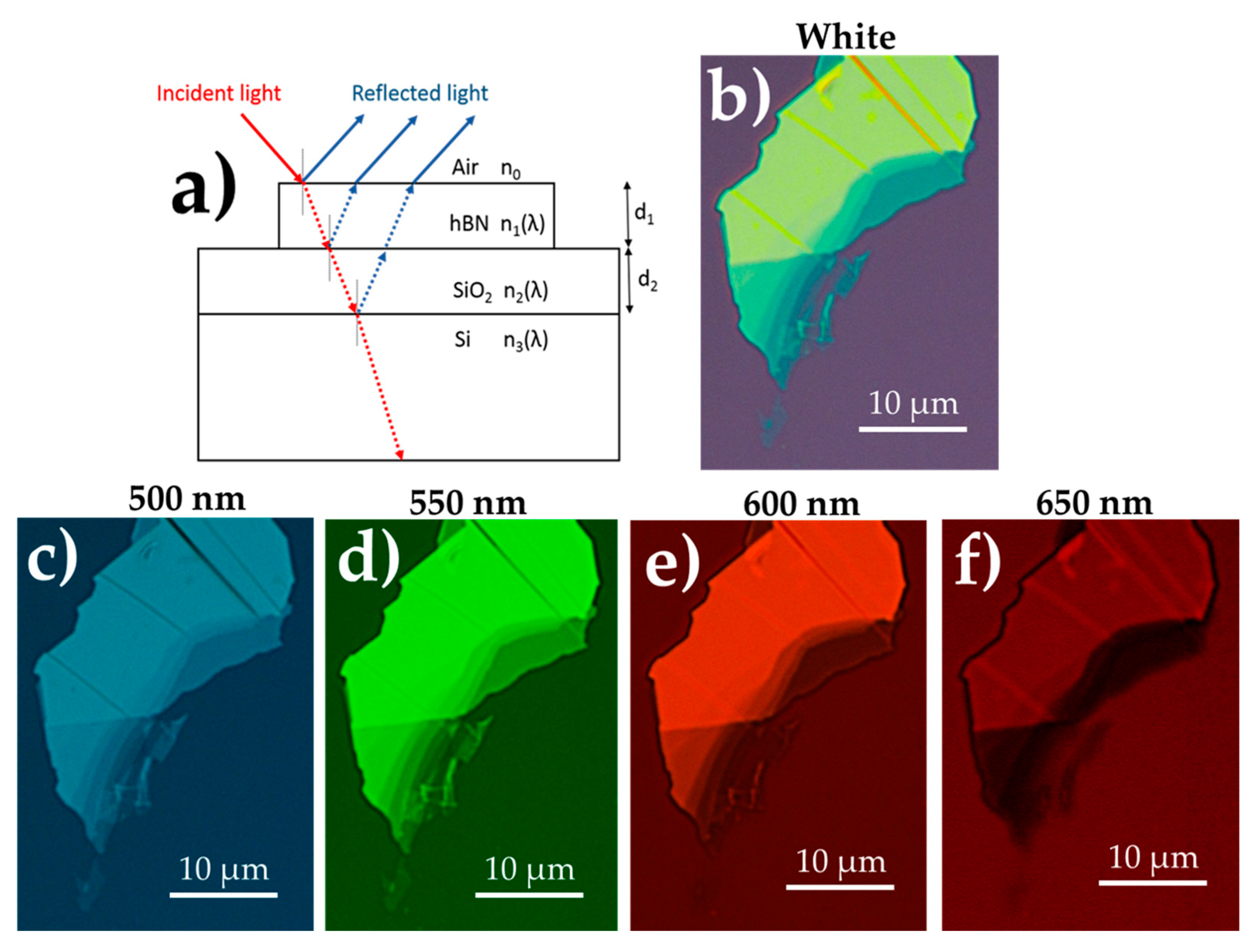
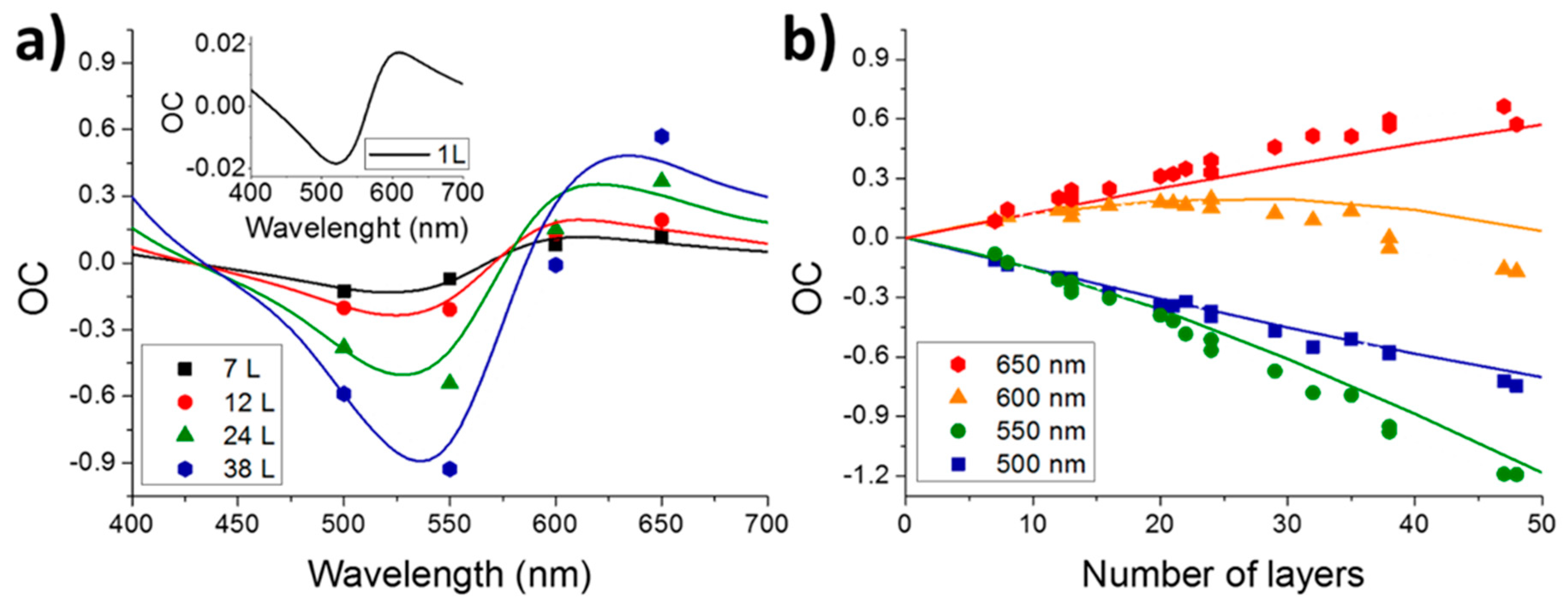
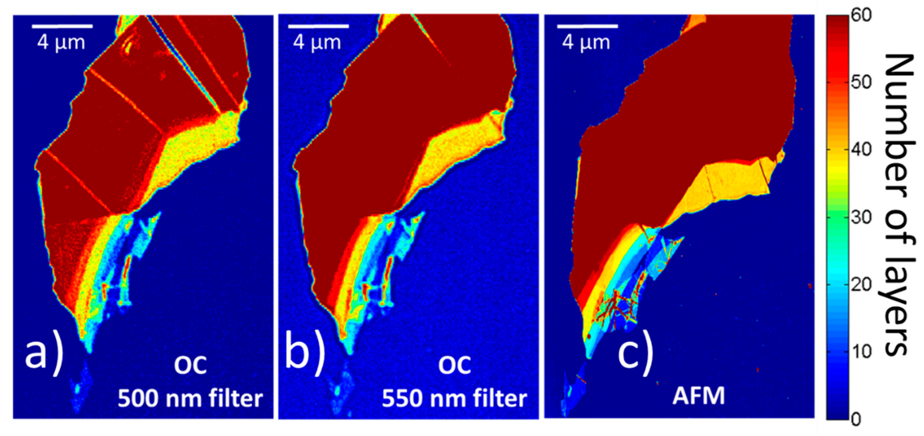
3.1. Optical Contrast Calculations
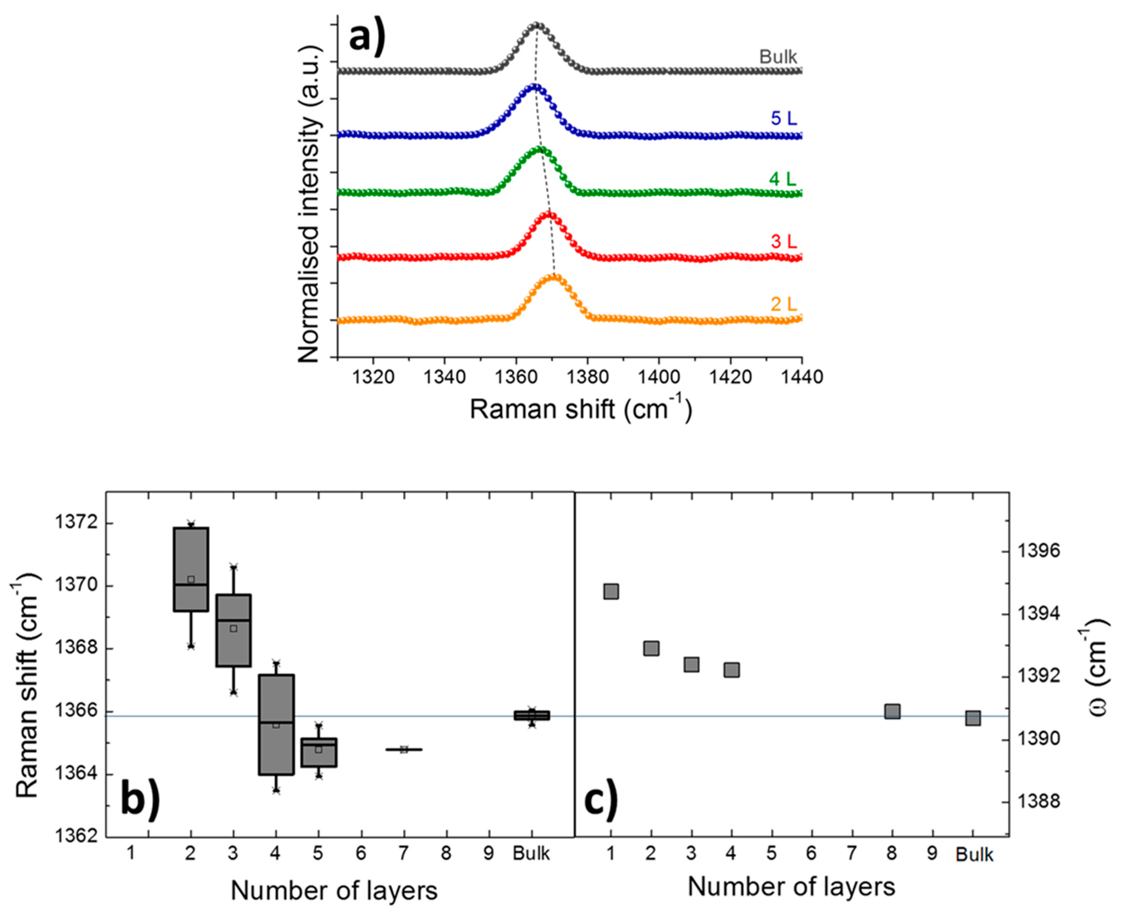
3.2. Raman Spectroscopy
4. Conclusions
Supplementary Materials
Author Contributions
Funding
Conflicts of Interest
References
- Zan, R.; Ramasse, Q.M.; Jalil, R.; Bangert, U. Atomic Structure of Graphene and h-BN Layers and Their Interactions with Metals. In Advances in Graphene Science; Aliofkhazraei, M., Ed.; InTech: London, UK, 2013; Chapter 1. [Google Scholar]
- Wang, J.; Ma, F.; Sun, M. Graphene, hexagonal boron nitride, and their heterostructures: Properties and applications. RSC Adv. 2017, 7, 16801. [Google Scholar] [CrossRef]
- Sajid, A.; Reimers, J.R.; Ford, M.J. Defect states in hexagonal boron nitride: Assignments of observed properties and prediction of properties relevant to quantum computation. Phys. Rev. 2018, 97, 064101. [Google Scholar] [CrossRef]
- McDougall, N.L.; Partridge, J.G.; Nicholls, R.J.; Russo, S.P.; McCulloch, D.G. Influence of point defects on the near edge structure of hexagonal boron nitride. Phys. Rev. 2017, 96, 144106. [Google Scholar] [CrossRef]
- Dean, C.R.; Young, A.F.; Meric, I.; Lee, C.; Wang, L.; Sorgenfrei, S.; Watanabe, K.; Taniguchi, T.; Kim, P.; Shepard, K.L.; et al. Boron nitride substrates for high-quality graphene electronics. Nat. Nanotechnol. 2010, 5, 722–726. [Google Scholar] [CrossRef] [PubMed]
- Exarhos, A.L.; Hopper, A.A.; Grote, R.R.; Alkauskas, A.; Bassett, L.C. Optical Signatures of Quantum Emitters in Suspended Hexagonal Boron Nitride. ACS Nano 2017, 11, 3328–3336. [Google Scholar] [CrossRef] [PubMed]
- Tran, T.T.; Elbadawi, C.; Totonjian, D.; Lobo, C.J.; Grosso, G.; Moon, H.; Englund, D.R.; Ford, M.J.; Aharonovich, I.; Toth, M. Robust Multicolor Single Photon Emission from Point Defects in Hexagonal Boron Nitride. ACS Nano 2016, 10, 7331–7338. [Google Scholar] [CrossRef] [PubMed]
- Cassabois, G.; Valvin, P.; Gil, B. Hexagonal boron nitride is an indirect bandgap semiconductor. Mater. Sci. 2016. [Google Scholar] [CrossRef]
- Paleari, F.; Galvani, T.; Amara, H.; Ducastelle, F.; Molina-Sánchez, A.; Wirtz, L. Excitons in few-layer hexagonal boron nitride: Davydov splitting and surface localization. 2D Mater. 2018, 5, 045017. [Google Scholar] [CrossRef]
- Paleari, F.; Miranda, H.P.C.; Molina-Sánchez, A.; Wirtz, L. Exciton-Phonon Coupling in the Ultraviolet Absorption and Emission Spectra of Bulk Hexagonal Boron Nitride. Phys. Rev. Lett. 2019, 122, 187401. [Google Scholar] [CrossRef]
- Kang, J.; Zhang, L.; Wei, S.H. A Unified Understanding of the Thickness-Dependent Bandgap Transition in Hexagonal Two-Dimensional Semiconductors. J. Phys. Chem. Lett. 2016, 7, 597–602. [Google Scholar] [CrossRef]
- Henck, H.; Pierucci, D.; Fugallo, G.; Avila, J.; Cassabois, G.; Dappe, Y.J.; Silly, M.G.; Chen, C.; Gil, B.; Gatti, M.; et al. Direct observation of the band structure in bulk hexagonal boron nitride. Phys. Rev. 2017, 95, 085410. [Google Scholar] [CrossRef]
- Bourrellier, R.; Meuret, S.; Tararan, A.; Stéphan, O.; Kociak, M.; Tizei, L.H.G.; Zobelli, A. Bright UV single photon emission at point defects in h-BN. Nano Lett. 2016, 16, 4317–4321. [Google Scholar] [CrossRef] [PubMed]
- Kubota, Y.; Watanabe, K.; Tsuda, O.; Taniguchi, T. Deep ultraviolet light-emitting hexagonal boron nitride synthesized at atmospheric pressure. Science 2007, 317, 932–934. [Google Scholar] [CrossRef] [PubMed]
- Li, L.H.; Chen, Y. Atomically Thin Boron Nitride: Unique Properties and Applications. Adv. Funct. Mater. 2016, 26, 2594–2608. [Google Scholar] [CrossRef]
- Roy, T.; Tosun, M.; Kang, J.S.; Sachid, A.B.; Desai, S.B.; Hettick, M.; Hu, C.C.; Javey, A. Field-Effect Transistors Built from All Two-Dimensional Material Components. ACS Nano 2014, 8, 6259–6264. [Google Scholar] [CrossRef] [PubMed]
- Lee, G.H.; Yu, Y.J.; Cui, X.; Petrone, N.; Lee, C.H.; Choi, M.S.; Lee, D.Y.; Lee, C.; Yoo, W.J.; Watanabe, K.; et al. Flexible and Transparent MoS2 Field-Effect Transistors on Hexagonal Boron Nitride-Graphene Heterostructures. ACS Nano 2013, 7, 7931–7936. [Google Scholar] [CrossRef]
- Britnell, L.; Gorbachev, R.V.; Jalil, R.; Belle, B.D.; Schedin, F.; Mishchenko, A.; Georgiou, T.; Katsnelson, M.I.; Eaves, L.; Morozov, S.V.; et al. Field-Effect Tunneling Transistor Based on Vertical Graphene Heterostructures. Science 2012, 335, 947–950. [Google Scholar] [CrossRef]
- Chen, C.C.; Li, Z.; Shi, L.; Cronin, S.B. Thermoelectric transport across graphene/hexagonal boron nitride/graphene heterostructures. Nano Res. 2015, 8, 666–672. [Google Scholar] [CrossRef]
- Ra, H.S.; Lee, A.Y.; Kwak, D.H.; Jeong, M.H.; Lee, J.S. Dual-Gate Black Phosphorus Field-Effect Transistors with Hexagonal Boron Nitride as Dielectric and Passivation Layers. ACS Appl. Mater. Interfaces 2018, 10, 925–932. [Google Scholar] [CrossRef]
- Li, M.Y.; Chen, C.H.; Shi, Y.; Li, L.J. Heterostructures based on two-dimensional layered materials and their potential applications. Mater. Today 2016, 19, 322–335. [Google Scholar] [CrossRef]
- Cai, Y.; Zhang, G.; Zhang, Y.W. The Electronic Properties of Phosphorene/Graphene and Phosphorene/Hexagonal Boron Nitride Heterostructures. J. Phys. Chem. C 2015, 119, 13929–13936. [Google Scholar] [CrossRef]
- Doganov, R.A.; O’Farrell, O.C.T.; Koenig, S.P.; Yeo, Y.; Ziletti, A.; Carvalho, A.; Campbell, D.K.; Coker, D.F.; Watanabe, K.; Taniguchi, T.; et al. Transport properties of pristine few-layer black phosphorus by van der Waals passivation in an inert atmosphere. Nat. Commun. 2015, 6, 6647. [Google Scholar] [CrossRef] [PubMed]
- Ahn, S.; Kim, G.; Nayak, P.K.; Yoon, S.I.; Lim, H. Prevention of Transition Metal Dichalcogenide Photodegradation by Encapsulation with hBN Layers. ACS Nano 2016, 10, 8973–8979. [Google Scholar] [CrossRef] [PubMed]
- Zhu, J.; Zhang, J.; Xu, S.; Hao, Y. Unintentional doping effects in black phosphorus by native vacancies in h-BN supporting layer. Appl. Surf. Sci. 2017, 402, 175–181. [Google Scholar] [CrossRef]
- Khan, A.F.; Brownson, D.A.C.; Randviir, E.P.; Smith, G.C.; Banks, C.E. 2D Hexagonal Boron Nitride (2D-hBN) Explored for the Electrochemical Sensing of Dopamine. Anal. Chem. 2016, 88, 9729–9737. [Google Scholar] [CrossRef] [PubMed]
- Khan, A.F.; Brownson, D.A.C.; Foster, C.V.; Smith, G.C.; Banks, C.E. Surfactant exfoliated 2D hexagonal Boron Nitride (2D-hBN) explored as a potential electrochemical sensor for dopamine: Surfactants significantly influence sensor capabilities. Analyst 2017, 142, 1756–1764. [Google Scholar] [CrossRef] [PubMed]
- Cai, Q.; Mateti, S.; Watanabe, K.; Taniguchi, T.; Huang, S.; Chen, Y.; Li, L.H. Boron Nitride Nanosheet-Veiled Gold Nanoparticles for Surface-Enhanced Raman Scattering. ACS Appl. Mater. Interfaces 2016, 8, 15630. [Google Scholar] [CrossRef] [PubMed]
- Dhanabalan, S.C.; Ponraj, J.S.; Guo, Z.; Li, S.; Bao, Q.; Zhang, H. Emerging Trends in Phosphorene Fabrication towards Next Generation Devices. Adv. Sci. 2017, 4, 1600305. [Google Scholar] [CrossRef]
- Liu, J.; Kutty, R.G.; Liu, Z. Controlled Synthesis of Atomically Layered Hexagonal Boron Nitride via Chemical Vapor Deposition. Molecules 2016, 21, 1636. [Google Scholar] [CrossRef]
- Sutter, P.; Lahiri, J.; Zahl, P.; Wang, B.; Sutter, E. Scalable Synthesis of Uniform Few-Layer Hexagonal Boron Nitride Dielectric Films. Nano Lett. 2013, 13, 276–281. [Google Scholar] [CrossRef]
- Nemes-Incze, P.; Osvath, Z.; Kamaras, K.; Biro, L.P. Anomalies in thickness measurements of graphene and few layer graphite crystals by tapping mode atomic force microscopy. Carbon 2008, 46, 1435–1442. [Google Scholar] [CrossRef]
- Wu, R.J.; Odlyzko, M.L.; Mkhoyan, K.A. Determining the thickness of atomically thin MoS2 and WS2 in the TEM. Ultramicroscopy 2014, 147, 8–20. [Google Scholar] [CrossRef] [PubMed]
- Ruppert, C.; Aslan, O.B.; Heinz, T.F. Optical Properties and Band Gap of Single- and Few-Layer MoTe2 Crystals. Nano Lett. 2014, 14, 6231–6236. [Google Scholar] [CrossRef] [PubMed]
- Yang, J.; Xu, R.; Pei, J.; Myint, Y.W.; Wang, F.; Wang, Z.; Zhang, S.; Yu, Z.; Lu, Y. Optical tuning of exciton and trion emissions in monolayer phosphorene. Light Sci. Appl. 2015, 4, 312. [Google Scholar] [CrossRef]
- Hajiyev, P.; Cong, C.; Qiu, C.; Yu, T. Contrast and Raman spectroscopy study of single- and few-layered charge density wave material: 2H-TaSe2. Sci. Rep. 2013, 3, 2593. [Google Scholar] [CrossRef] [PubMed]
- Stenger, I.; Schué, L.; Boukhicha, M.; Berini, B.; Plaçais, B.; Loiseau, A.; Barjon, J. Low frequency Raman spectroscopy of few-atomic-layer thick hBN crystals. 2D Mater. 2017, 4, 031003. [Google Scholar] [CrossRef]
- Brotons-Gisbert, M.; Sánchez-Royo, J.F.; Martínez-Pastor, J.P. Thickness identification of atomically thin InSe nanoflakes on SiO2/Sisubstrates by optical contrast analysis. Appl. Surf. Sci. 2015, 354, 453–458. [Google Scholar] [CrossRef]
- Li, X.L.; Han, W.P.; Wu, J.B.; Qiao, X.F.; Zhang, J.; Tan, P.H. Layer-Number Dependent Optical Properties of 2D Materials and Their Application for Thickness Determination. Adv. Funct. Mater. 2017, 27, 1604468. [Google Scholar] [CrossRef]
- Golla, D.; Chattrakun, K.; Watanabe, K.; Taniguchi, T.; LeRoy, B.J.; Sandhu, A. Optical thickness determination of hexagonal Boron Nitride. Appl. Phys. Lett. 2013, 102, 161906. [Google Scholar] [CrossRef]
- Wang, Y.Y.; Gao, R.X.; Ni, Z.H.; He, H.; Guo, S.P.; Yang, H.P.; Cong, C.X.; Yu, T. Thickness identification of two-dimensional materials by optical imaging. Nanotechnology 2012, 23, 495713. [Google Scholar] [CrossRef]
- Brotons-Gisbert, M.; Andres-Penares, D.; Martínez-Pastor, J.P.; Cros, A.; Sánchez-Royo, J.F. Optical contrast of 2D InSe on SiO2/Si and transparent substrates using bandpass filters. Nanotechnology 2017, 28, 115706. [Google Scholar] [CrossRef] [PubMed]
- Gorbachev, R.V.; Riaz, I.; Nair, R.R.; Jalil, R.; Britnell, L.; Belle, B.D.; Hill, E.Q.; Novoselov, K.S.; Watanabe, K.; Taniguchi, T.; et al. Hunting for Monolayer Boron Nitride: Optical and Raman Signatures. Small 2011, 7, 465–468. [Google Scholar] [CrossRef] [PubMed]
- Cai, Q.; Scullion, D.; Falin, A.; Watanabe, K.; Taniguchi, T.; Chen, Y.; Santos, E.J.G.; Lia, L.H. Raman signature and phonon dispersion of atomically thin boron nitride. Nanoscale 2017, 9, 3059–3067. [Google Scholar] [CrossRef] [PubMed]
- Bing, D.; Wang, Y.; Bai, J.; Du, R.; Wu, G.; Liu, L. Optical contrast for identifying the thickness of two-dimensional materials. Opt. Commun. 2018, 406, 128–138. [Google Scholar] [CrossRef]
- Lee, J.U.; Kim, M.; Cheong, H. Raman Spectroscopic Studies on Two-Dimensional Materials. Appl. Microsc. 2015, 45, 126–130. [Google Scholar] [CrossRef]
- Reich, S.; Ferrari, A.C. Resonant Raman scattering in cubic and hexagonal boron nitride. Phys. Rev. B 2005, 71, 205201. [Google Scholar] [CrossRef]
- Arenal, R.; Ferrari, A.C.; Reich, S.; Wirtz, L.; Mevellec, J.Y.; Lefrant, S.; Rubio, A.; Loiseau, A. Raman Spectroscopy of Single-Wall Boron Nitride Nanotubes. Nano Lett. 2006, 6, 1812–1816. [Google Scholar] [CrossRef] [PubMed]
- Bissett, M.A.; Tsuji, M.; Ago, H. Strain engineering the properties of graphene and other two-dimensional crystals. Phys. Chem. Chem. Phys. 2014, 16, 11124. [Google Scholar] [CrossRef]
- Zandiatashbar, A.; Lee, G.H.; An, S.J.; Lee, S.; Mathew, N.; Terrones, M.; Hayashi, T.; Picu, C.R.; Hone, J.; Koratkar, N. Effect of defects on the intrinsic strength and stiffness of graphene. Nat. Commun. 2014, 5, 3186. [Google Scholar] [CrossRef]
- Cançado, L.G.; Gomes da Silva, M.; Ferreira, E.H.M.; Hof, F.; Kampioti, K.; Huang, K.; Pénicaud, A.; Achete, C.A.; Capaz, R.B.; Jorio, A. Disentangling contributions of point and line defects in the Raman spectra of graphene-related materials. 2D Mater. 2017, 4, 025039. [Google Scholar] [CrossRef]
- Chen, Z.; Darancet, P.; Wang, L.; Crowther, A.C.; Gao, Y.; Dean, C.R.; Taniguchi, T.; Watanabe, K.; Hone, J.; Marianetti, C.A.; et al. Physical Adsorption and Charge Transfer of Molecular Br2 on Graphene. ACS Nano 2014, 8, 2943–2950. [Google Scholar] [CrossRef] [PubMed]
- Li, L.H.; Cervenka, J.; Watanabe, K.; Taniguchi, T.; Chen, Y. Strong oxidation resistance of atomically thin boron nitride nanosheets. ACS Nano 2014, 8, 1457–1462. [Google Scholar] [CrossRef] [PubMed]
- Li, X.; Liu, J.; Ding, K.; Zhao, X.; Li, S.; Zhou, W.; Liang, B. Temperature Dependence of Raman-Active In-Plane E2g Phonons in Layered Graphene and h-BN Flakes. Nanoscale Res. Lett. 2018, 13, 25. [Google Scholar] [CrossRef] [PubMed]
- Giannozzi, P.; Baroni, S.; Bonini, N.; Calandra, M.; Car, R.; Cavazzoni, C.; Ceresoli, D.; Chiarotti, G.L.; Cococcioni, M.; Dabo, I.; et al. QUANTUM ESPRESSO: A modular and open-source software project for quantum simulations of materials. J. Phys. Condens. Matter 2009, 21, 395502. [Google Scholar] [CrossRef] [PubMed]


© 2019 by the authors. Licensee MDPI, Basel, Switzerland. This article is an open access article distributed under the terms and conditions of the Creative Commons Attribution (CC BY) license (http://creativecommons.org/licenses/by/4.0/).
Share and Cite
Krečmarová, M.; Andres-Penares, D.; Fekete, L.; Ashcheulov, P.; Molina-Sánchez, A.; Canet-Albiach, R.; Gregora, I.; Mortet, V.; Martínez-Pastor, J.P.; Sánchez-Royo, J.F. Optical Contrast and Raman Spectroscopy Techniques Applied to Few-Layer 2D Hexagonal Boron Nitride. Nanomaterials 2019, 9, 1047. https://doi.org/10.3390/nano9071047
Krečmarová M, Andres-Penares D, Fekete L, Ashcheulov P, Molina-Sánchez A, Canet-Albiach R, Gregora I, Mortet V, Martínez-Pastor JP, Sánchez-Royo JF. Optical Contrast and Raman Spectroscopy Techniques Applied to Few-Layer 2D Hexagonal Boron Nitride. Nanomaterials. 2019; 9(7):1047. https://doi.org/10.3390/nano9071047
Chicago/Turabian StyleKrečmarová, Marie, Daniel Andres-Penares, Ladislav Fekete, Petr Ashcheulov, Alejandro Molina-Sánchez, Rodolfo Canet-Albiach, Ivan Gregora, Vincent Mortet, Juan P. Martínez-Pastor, and Juan F. Sánchez-Royo. 2019. "Optical Contrast and Raman Spectroscopy Techniques Applied to Few-Layer 2D Hexagonal Boron Nitride" Nanomaterials 9, no. 7: 1047. https://doi.org/10.3390/nano9071047
APA StyleKrečmarová, M., Andres-Penares, D., Fekete, L., Ashcheulov, P., Molina-Sánchez, A., Canet-Albiach, R., Gregora, I., Mortet, V., Martínez-Pastor, J. P., & Sánchez-Royo, J. F. (2019). Optical Contrast and Raman Spectroscopy Techniques Applied to Few-Layer 2D Hexagonal Boron Nitride. Nanomaterials, 9(7), 1047. https://doi.org/10.3390/nano9071047