Device Engineering for All-Inorganic Perovskite Light-Emitting Diodes


Abstract
1. Introduction
2. Fundamental Concepts of All-Inorganic PeLEDs
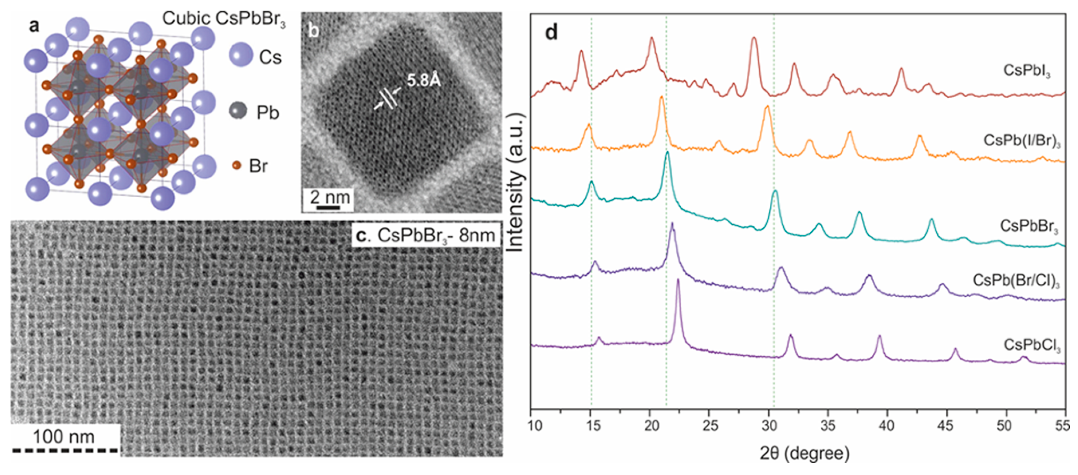
2.1. All-Inorganic Perovskite Emitters
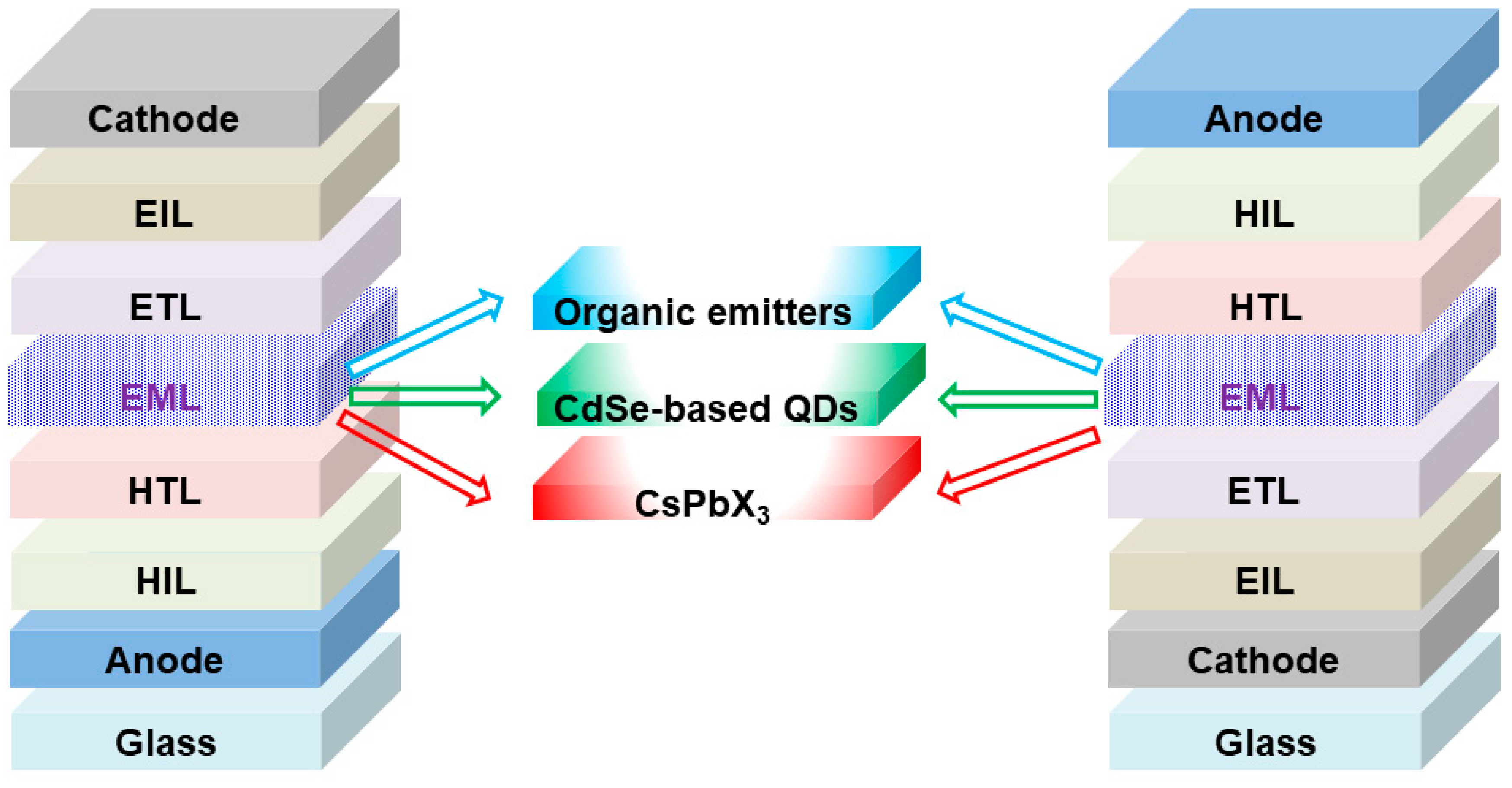
2.2. Device Architectures
3. The Device Engineering in All-Inorganic PeLEDs
3.1. Basic Aspects of Device Engineering
3.2. Emergence of All-Inorganic PeLEDs
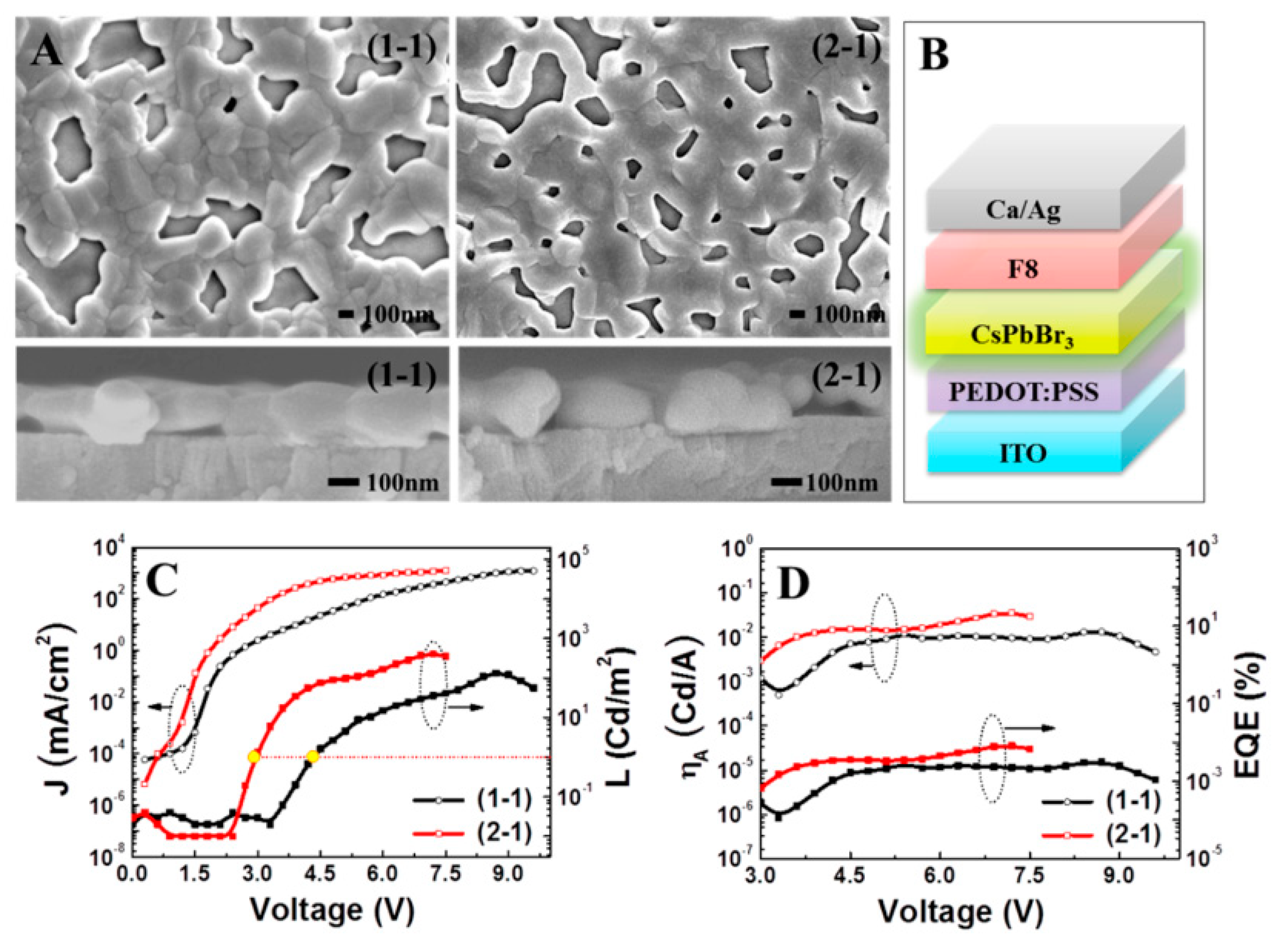
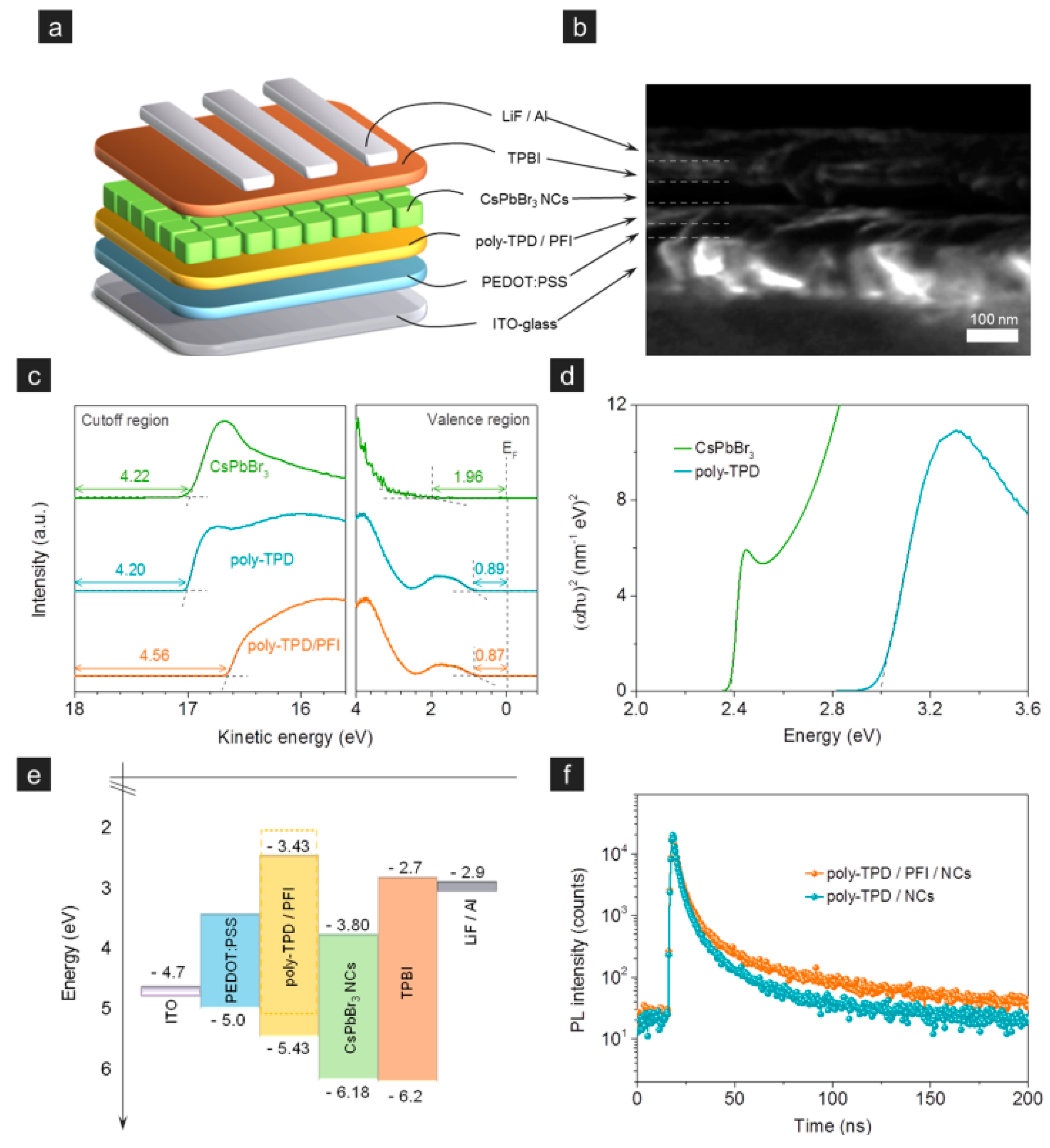
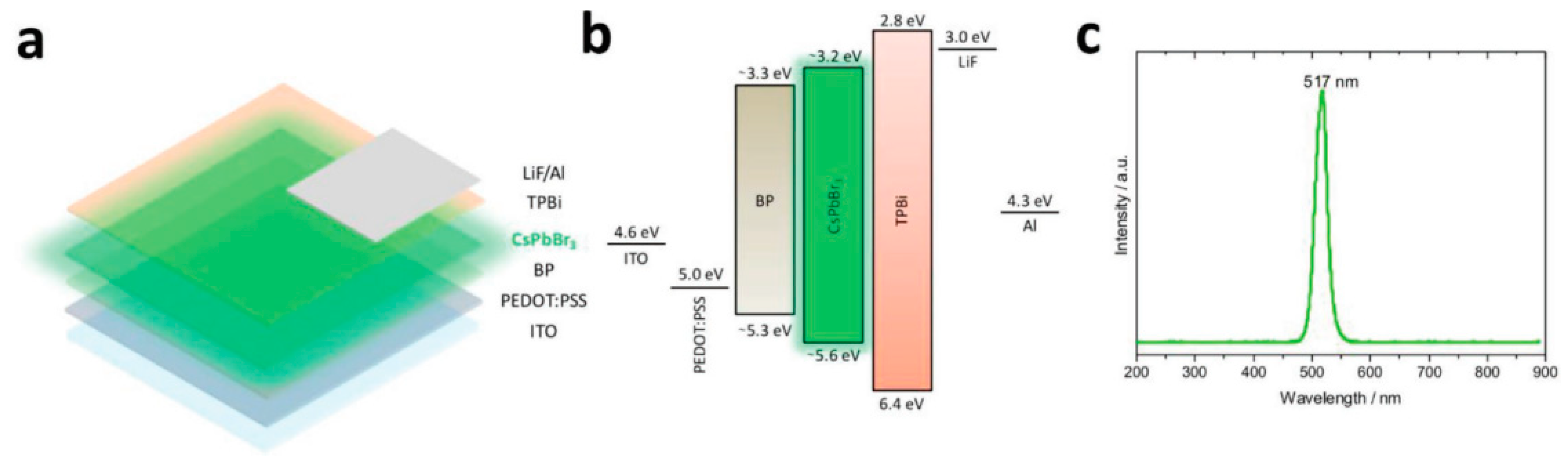
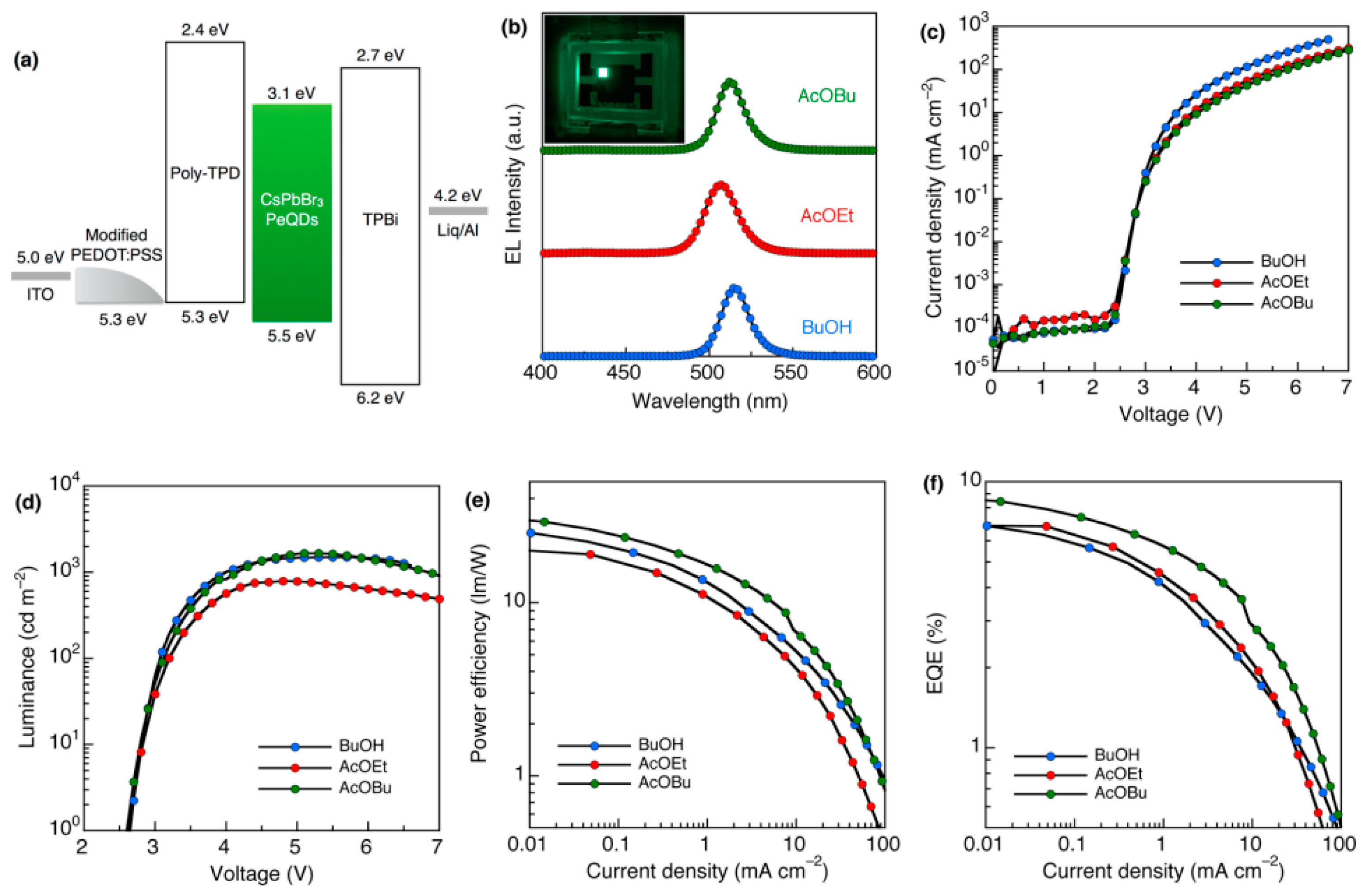
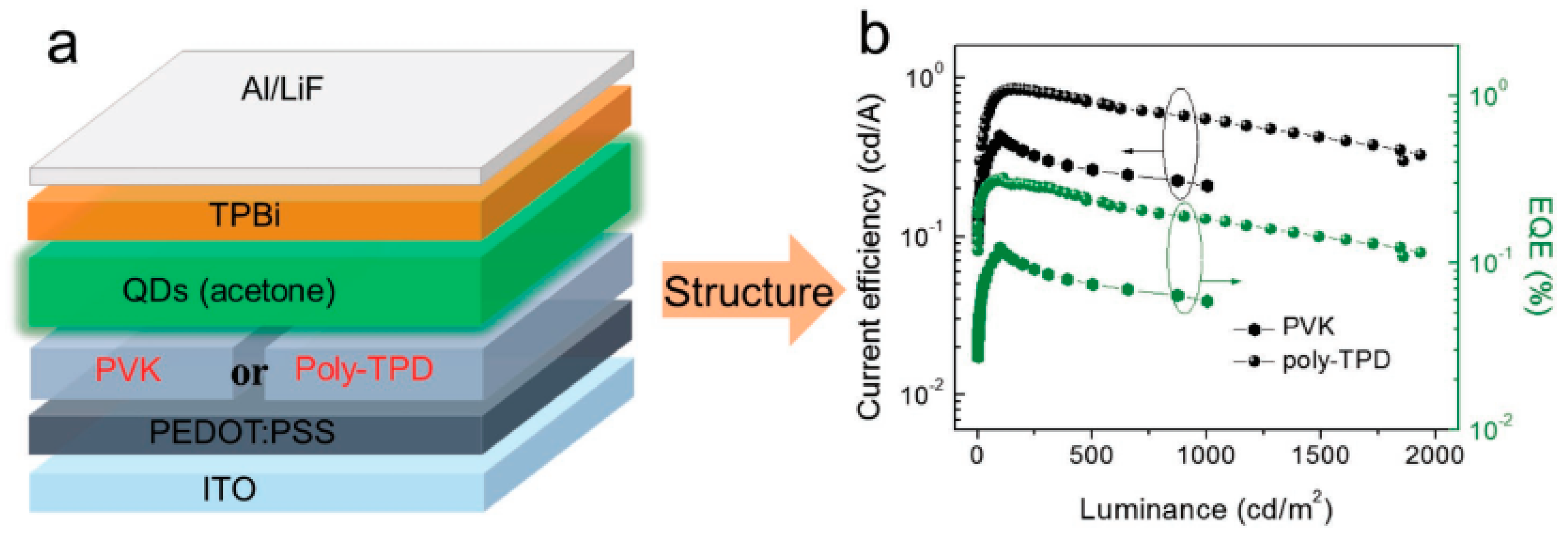
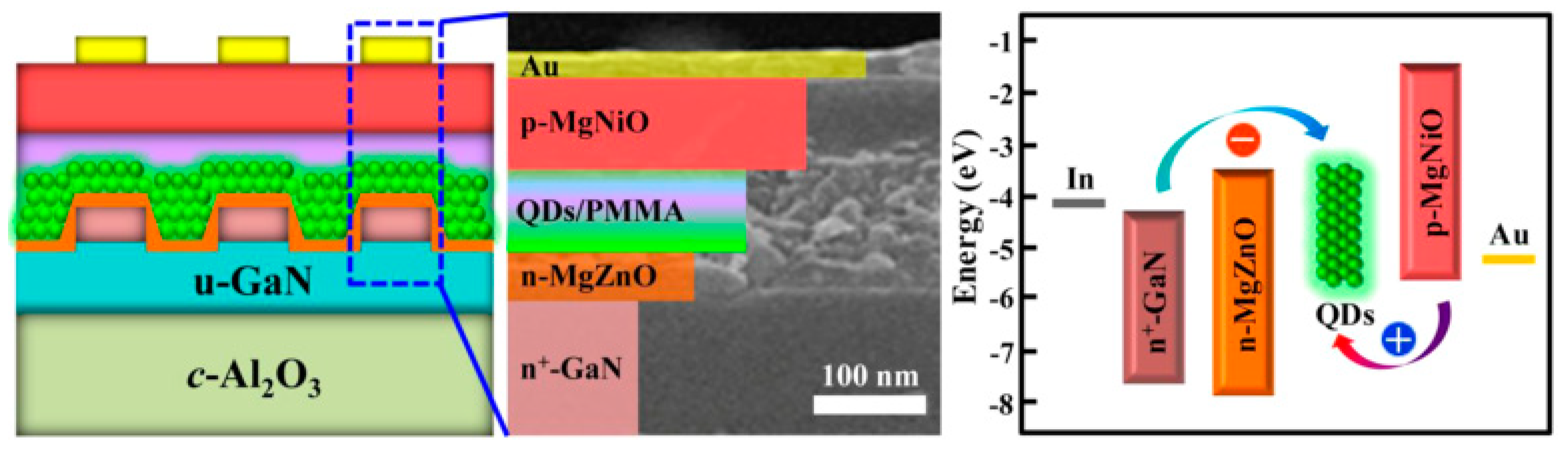
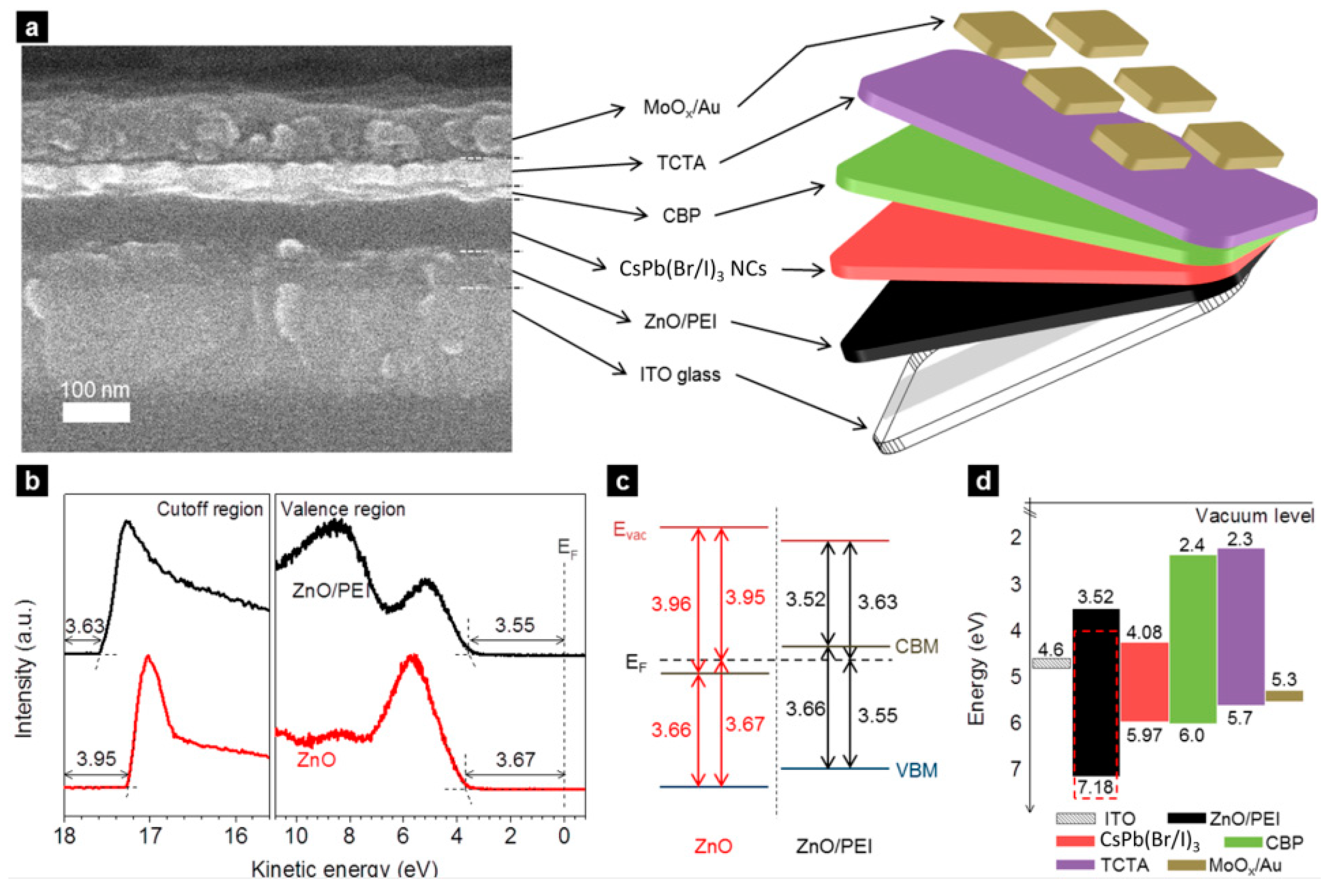
3.3. Strategies to Improve the Hole Injection
3.4. Approaches to Enhance the Electron Injection
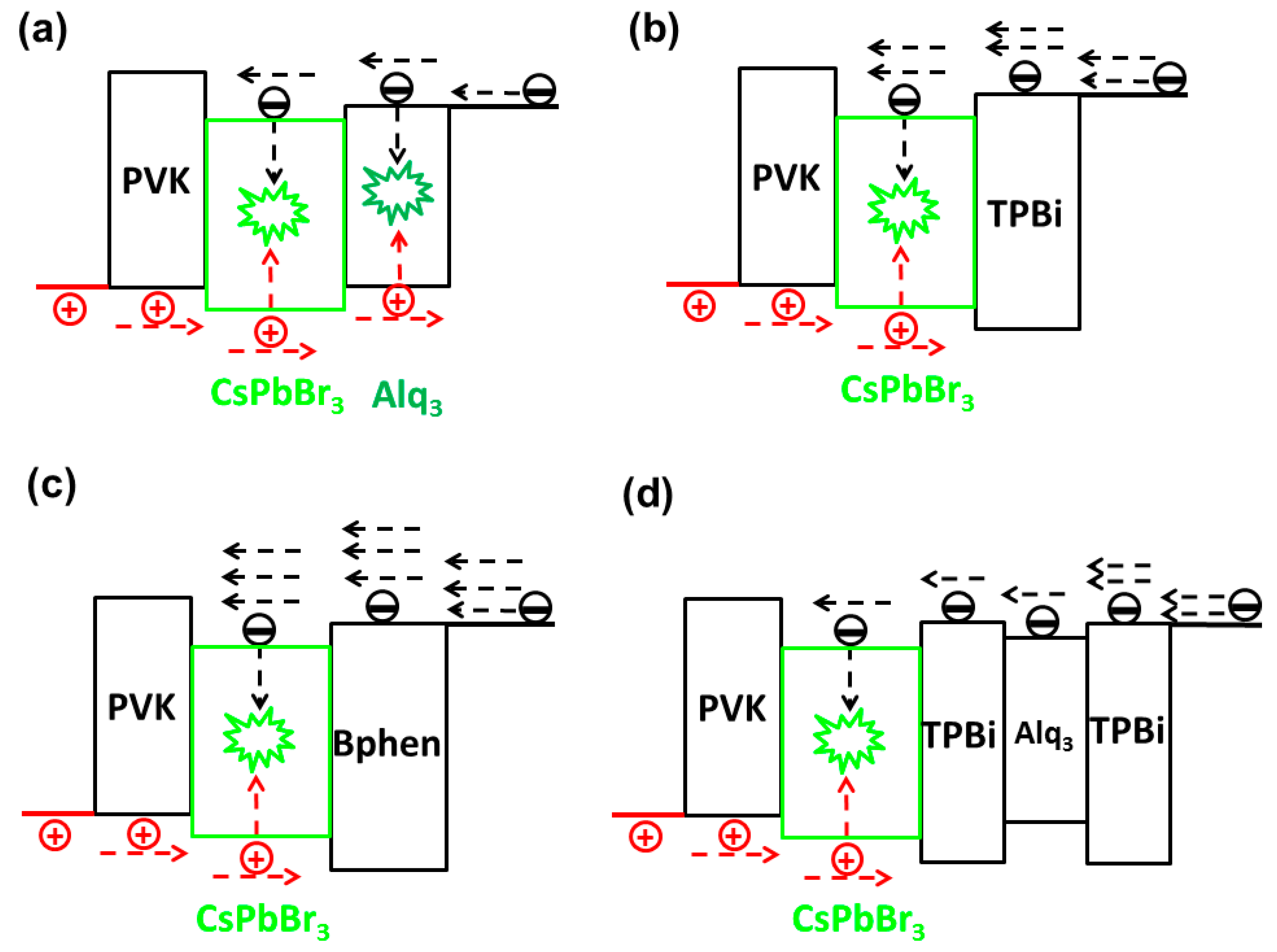
3.5. Schemes to Increase the Charge Balance
3.6. Methods to Decrease the Charge Leakage
4. Summary and Outlook
Author Contributions
Funding
Conflicts of Interest
References
- Lee, M.M.; Teuscher, J.; Miyasaka, T.; Murakami, T.N.; Snaith, H.J. Efficient Hybrid Solar Cells Based on Meso-Superstructured Organometal Halide Perovskites. Science 2012, 338, 643–647. [Google Scholar] [CrossRef] [PubMed]
- Luo, J.; Im, J.H.; Mayer, M.T.; Schreier, M.; Nazeeruddin, M.K.; Park, N.G.; Tilley, S.D.; Fan, H.J.; Grätzel, M. Water photolysis at 12.3% efficiency via perovskite photovoltaics and Earth-abundant catalysts. Science 2014, 345, 1593–1596. [Google Scholar] [CrossRef] [PubMed]
- Jeon, N.J.; Noh, J.H.; Yang, W.S.; Kim, Y.C.; Ryu, S.; Seo, J.; Seok, S.I. Compositional engineering of perovskite materials for high-performance solar cells. Nature 2015, 517, 476–480. [Google Scholar] [CrossRef] [PubMed]
- Zhu, H.; Fu, Y.; Meng, F.; Wu, X.; Gong, Z.; Ding, Q.; Gustafsson, M.V.; Trinh, M.T.; Jin, S.; Zhu, X.Y. Lead halide perovskite nanowire lasers with low lasing thresholds and high quality factors. Nat. Mater. 2015, 14, 636–642. [Google Scholar] [CrossRef] [PubMed]
- Sutherland, B.R.; Sargent, E.H. Perovskite photonic sources. Nat. Photonics 2016, 10, 295–302. [Google Scholar] [CrossRef]
- Stranks, S.D.; Snaith, H.J. Metal-halide perovskites for photovoltaic and light-emitting devices. Nat. Nanotechnol. 2015, 10, 391–402. [Google Scholar] [CrossRef]
- Huang, H.; Polavarapu, L.; Sichert, J.A.; Susha, A.S.; Urban, A.S.; Rogach, A.L. Colloidal lead halide perovskite nanocrystals: Synthesis, optical properties and applications. NPG Asia Mater. 2016, 8, e328. [Google Scholar] [CrossRef]
- Protesescu, L.; Yakunin, S.; Bodnarchuk, M.I.; Krieg, F.; Caputo, R.; Hendon, C.H.; Yang, R.X.; Walsh, A.; Kovalenko, M.V. Nanocrystals of Cesium Lead Halide Perovskites (CsPbX3, X = Cl, Br, and I): Novel Optoelectronic Materials Showing Bright Emission with Wide Color Gamut. Nano Lett. 2015, 15, 3692–3696. [Google Scholar] [CrossRef]
- Huang, H.; Susha, A.S.; Kershaw, S.V.; Hung, T.F.; Rogach, A.L. Control of emission color of high quantum yield CH3NH3PbBr3 perovskite quantum dots by precipitation temperature. Adv. Sci. 2015, 2, 1500194. [Google Scholar] [CrossRef]
- Cho, H.; Jeong, S.-H.; Park, M.-H.; Kim, Y.-H.; Wolf, C.; Lee, C.-L.; Heo, J.H.; Sadhanala, A.; Myoung, N.; Yoo, S.; et al. Overcoming the electroluminescence efficiency limitations of perovskite light-emitting diodes. Science 2015, 350, 1222–1225. [Google Scholar] [CrossRef]
- Kim, Y.-H.; Cho, H.; Heo, J.H.; Kim, T.-S.; Myoung, N.; Lee, C.-L.; Im, S.H.; Lee, T.-W. Multicolored Organic/Inorganic Hybrid Perovskite Light-Emitting Diodes. Adv. Mater. 2015, 27, 1248–1254. [Google Scholar] [CrossRef] [PubMed]
- Kim, Y.-H.; Cho, H.; Lee, T.-W. Metal halide perovskite light emitters. Proc. Natl. Acad. Sci. USA 2016, 113, 11694–11702. [Google Scholar] [CrossRef] [PubMed]
- Wang, N.; Cheng, L.; Ge, R.; Zhang, S.; Miao, Y.; Zou, W.; Yi, C.; Sun, Y.; Cao, Y.; Yang, R.; et al. Perovskite light-emitting diodes based on solution-processed self-organized multiple quantum wells. Nat. Photonics 2016, 10, 699–704. [Google Scholar] [CrossRef]
- Park, M.-H.; Jeong, S.-H.; Seo, H.-K.; Wolf, C.; Kim, Y.-H.; Kim, H.; Byun, J.; Kim, J.S.; Cho, H.; Lee, T.-W. Unravelling Additive-based Nanocrystal Pinning for High Efficiency Organic-Inorganic Halide Perovskite Light-Emitting Diodes. Nano Energy 2017, 42, 157–165. [Google Scholar] [CrossRef]
- Zhou, Y.; Zhao, Y. Chemical stability and instability of inorganic halide perovskites. Energy Environ. Sci. 2019, 12, 1495. [Google Scholar] [CrossRef]
- Tan, Z.K.; Moghaddam, R.S.; Lai, M.L.; Docampo, P.; Higler, R.; Deschler, F.; Price, M.; Sadhanala, A.L.; Pazos, M.; Credgington, D.; et al. Bright light-emitting diodes based on organometal halide perovskite. Nat. Nanotechnol. 2014, 9, 687–692. [Google Scholar] [CrossRef] [PubMed]
- Lin, K.; Xing, J.; Quan, L.N.; Arquer, F.P.G.; Gong, X.; Lu, J.; Xie, L.; Zhao, W.; Zhang, D.; Yan, C.; et al. Perovskite light-emitting diodes with external quantum efficiency exceeding 20 per cent. Nature 2018, 562, 245–248. [Google Scholar] [CrossRef]
- Cao, Y.; Wang, N.; Tian, H.; Guo, J.; Wei, Y.; Chen, H.; Miao, Y.; Zou, W.; Pan, K.; He, Y.; et al. Perovskite light-emitting diodes based on spontaneously formed submicrometre-scale structures. Nature 2018, 562, 249–253. [Google Scholar] [CrossRef]
- Song, J.; Li, J.; Li, X.; Xu, L.; Dong, Y.; Zeng, H. Quantum Dot Light-Emitting Diodes Based on Inorganic Perovskite Cesium Lead Halides (CsPbX3). Adv. Mater. 2016, 27, 7162–7167. [Google Scholar] [CrossRef]
- Wei, S.; Yang, Y.; Kang, X.; Wang, L.; Huang, L.; Pan, D. Homogeneous Synthesis and Electroluminescence Device of Highly Luminescent CsPbBr\r3\r Perovskite Nanocrystals. Inorg. Chem. 2017, 56, 2596–2601. [Google Scholar] [CrossRef]
- Yettapu, G.R.; Talukdar, D.; Sarkar, S.; Swarnkar, A.; Nag, A.; Ghosh, P.; Mandal, P. THz conductivity within colloidal CsPbBr\r3\r perovskite nanocrystals: Remarkably high carrier mobilities and large diffusion lengths. Nano Lett. 2016, 16, 4838–4848. [Google Scholar] [CrossRef] [PubMed]
- Swarnkar, A.; Marshall, A.R.; Sanehira, E.M.; Chernomordik, B.D.; Moore, D.T.; Christians, J.A.; Chakrabarti, T.; Luther, J.M. Quantum Dot-Induced Phase Stabilization Of Σ-Cspbi3 Perovskite for High-Efficiency Photovoltaics. Science 2016, 354, 9295. [Google Scholar] [CrossRef] [PubMed]
- Wang, Z.; Luo, Z.; Zhao, C.; Guo, Q.; Wang, Y.; Wang, F.; Bian, X.; Alsaedi, A.; Hayat, T.; Tan, Z. Efficient and Stable Pure Green All-Inorganic Perovskite CsPbBr3 Light-Emitting Diodes with a Solution-Processed NiOx Interlayer. J. Phys. Chem. C 2017, 121, 28132–28138. [Google Scholar] [CrossRef]
- Jeong, B.; Han, H.; Choi, Y.J.; Cho, S.H.; Kim, E.H.; Lee, S.W.; Kim, J.S.; Park, C.; Kim, D.; Park, C. Inorganic CsPbI3 Perovskite Phase-Stabilized by Poly(ethylene oxide) for Red-Light-Emitting Diodes. Adv. Funct. Mater. 2018, 28, 1706401. [Google Scholar] [CrossRef]
- Song, P.; Qiao, B.; Song, D.; Liang, Z.; Gao, D.; Cao, J.; Shen, Z.; Xu, Z.; Zhao, S. Colour- and structure-stable CsPbBr3CsPb2r5compounded quantum dots with tuneable blue and green light emission. J. Alloy. Compd. 2018, 767, 98–105. [Google Scholar] [CrossRef]
- Ng, Y.F.; Neo, W.J.; Jamaludin, N.F.; Yantara, N.; Mhaisalkar, S.; Mathews, N. Enhanced Coverage of All-Inorganic Perovskite CsPbBr3 through Sequential Deposition for Green Light-Emitting Diodes. Energy. Technol. 2017, 5, 1859–1865. [Google Scholar] [CrossRef]
- Wu, Z.; Wei, J.; Sun, Y.; Wu, J.; Hou, Y.; Wang, P.; Wang, N.; Zhao, Z. Air-stable all-inorganic perovskite quantum dot inks for multicolor patterns and white LEDs. J. Mater. Sci. 2019, 54, 6917–6929. [Google Scholar]
- Wu, H.; Zhang, Y.; Lu, M.; Zhang, X.; Sun, C.; Zhang, T.; Colvin, V.L.; Yu, W.W. Surface ligand modification of cesium lead bromide nanocrystals for improved light-emitting performance. Nanoscale 2018, 10, 4173–4178. [Google Scholar] [CrossRef]
- Park, J.H.; Lee, A.-Y.; Yu, J.C.; Nam, Y.S.; Choi, Y.; Park, J.; Song, M.h. Surface Ligand Engineering for Efficient Perovskite Nanocrystal-Based Light-Emitting Diodes. ACS Appl. Mater. Interfaces 2019, 11, 8428–8435. [Google Scholar] [CrossRef]
- Cheng, L.-P.; Huang, J.-S.; Shen, Y.; Li, G.-P.; Liu, X.-K.; Li, W.; Wang, Y.-H.; Li, Y.-Q.; Jiang, Y.; Gao, F.; et al. Efficient CsPbBr3 Perovskite Light-Emitting Diodes Enabled by Synergetic Morphology Control. Adv. Opt. Mater. 2019, 7, 1801534. [Google Scholar] [CrossRef]
- Wang, K.-H.; Zhu, B.-S.; Yao, J.-S.; Yao, H.-B. Chemical regulation of metal halide perovskite nanomaterials for efficient light-emitting diodes. Sci. Chin. Chem. 2018, 61, 1047–1061. [Google Scholar] [CrossRef]
- Si, J.; Liu, Y.; He, Z.; Du, H.; Du, K.; Chen, D.; Li, J.; Xu, M.; Tian, H.; He, H.; et al. Efficient and High-Color-Purity Light-Emitting Diodes Based on In-Situ Grown Films of CsPbX3 (X = Br, I) Nanoplates with Controlled Thicknesses. ACS Nano 2017, 11, 11100–11107. [Google Scholar] [CrossRef] [PubMed]
- Sasaki, H.; Kamata, N.; Honda, Z.; Yasuda, T. Improved thermal stability of CsPbBr3 quantum dots by ligand exchange and their application to light-emitting diodes. Appl. Phys. Express 2019, 12, 035004. [Google Scholar] [CrossRef]
- Song, L.; Guo, X.; Hu, Y.; Lv, Y.; Lin, J.; Fan, Y.; Zhang, N.; Liu, X. Improved performance of CsPbBr3 perovskite light-emitting devices by both boundary and interface defects passivation. Nanoscale 2018, 10, 18315–18322. [Google Scholar] [CrossRef] [PubMed]
- Wu, S.; Zhao, S.; Xu, Z.; Song, D.; Qiao, B.; Yue, H.; Yang, J.; Zheng, X.; Wei, P. Highly bright and stable all-inorganic perovskite light-emitting diodes with methoxypolyethylene glycols modified CsPbBr3 emission layer. Appl. Phys. Lett. 2018, 113, 213501. [Google Scholar] [CrossRef]
- Chiba, T.; Hayashi, Y.; Ebe, H.; Hoshi, K.; Sato, J.; Sato, S.; Pu, Y.-J.; Ohisa, S.; Kido, J. Anion-exchange red perovskite quantum dots with ammonium iodine salts for highly efficient light-emitting devices. Nat. Photonics 2018, 12, 681–687. [Google Scholar] [CrossRef]
- Yang, X.; Zhou, G.; Wong, W.-Y. Functionalization of Phosphorescent Emitters and Their Host Materials by Main-Group Elements for Phosphorescent Organic Light-Emitting Devices. Chem. Soc. Rev. 2015, 44, 8484–8575. [Google Scholar] [CrossRef]
- Nishimoto, T.; Yasuda, T.; Lee, S.Y.; Kondo, R.; Adachi, C. A Six-carbazole-decorated Cyclophosphazene as a Host with High Triplet Energy to Realize Efficient Delayed-Fluorescence OLEDs. Mater. Horiz. 2014, 1, 264–269. [Google Scholar] [CrossRef]
- Liu, B.; Li, X.; Tao, H.; Zou, J.; Xu, M.; Wang, L.; Peng, J.; Cao, Y. Manipulation of Exciton Distribution for High-Performance Fluorescent/Phosphorescent Hybrid White Organic Light-Emitting Diodes. J. Mater. Chem. C 2017, 5, 7668–7683. [Google Scholar] [CrossRef]
- Luo, D.; Xiao, P.; Liu, B. Doping-Free White Organic Light-Emitting Diodes. Chem. Rec. 2018, 18, 1–16. [Google Scholar] [CrossRef]
- Fan, C.; Yang, C. Yellow/orange emissive heavy-metal complexes asphosphors in monochromatic and white organic light-emitting devices. Chem. Soc. Rev. 2014, 43, 6439–6469. [Google Scholar] [CrossRef] [PubMed]
- Dai, X.L.; Zhang, Z.X.; Jin, Y.Z.; Niu, Y.; Cao, H.J.; Liang, X.Y.; Chen, L.W.; Wang, J.P.; Peng, X.G. Solution-Processed, High Performance Light-Emitting Diodes Based on Quantum Dots. Nature 2014, 515, 96–100. [Google Scholar] [CrossRef] [PubMed]
- Mashford, B.S.; Stevenson, M.; Popovic, Z.; Hamilton, C.; Zhou, Z.; Breen, C.; Steckel, J.; Bulovic, V.; Bawendi, M.; Coe-Sullivan, S.; et al. High-efficiency quantum-dot light-emitting devices with enhanced charge injection. Nat. Photonics 2013, 7, 407–412. [Google Scholar] [CrossRef]
- Shirasaki, Y.; Supran, G.J.; Bawendi, M.G.; Bulović, V. Emergence of colloidal quantum-dot light-emitting technologies. Nat. Photonics 2013, 7, 13–23. [Google Scholar] [CrossRef]
- Yang, Y.X.; Zheng, Y.; Cao, W.R.; Titov, A.; Hyvonen, J.; Manders, J.R.; Xue, J.G.; Holloway, P.H.; Qian, L. High-Efficiency Light-Emitting Devices Based on Quantum Dots with Tailored Nanostructures. Nat. Photonics 2015, 9, 259–266. [Google Scholar] [CrossRef]
- Shen, H.; Gao, Q.; Zhang, Y.; Lin, Y.; Lin, Q.L.; Li, Z.; Chen, L.; Zeng, Z.; Li, X.; Jia, Y.; et al. Visible quantum dot light-emitting diodes with simultaneous high brightness and efficiency. Nat. Photonics 2019, 13, 192–197. [Google Scholar] [CrossRef]
- Chiba, T.; Hoshi, K.; Pu, Y.-J.; Takeda, Y.; Hayashi, Y.; Ohisa, S.; Kawata, S.; Kido, J. High-Efficiency Perovskite Quantum-Dot Light-Emitting Devices by Effective Washing Process and Interfacial Energy Level Alignment. ACS Appl. Mater. Interfaces 2017, 9, 18054–18060. [Google Scholar] [CrossRef]
- Hoshi, K.; Chiba, T.; Sato, J.; Hayashi, Y.; Takahashi, Y.; Ebe, H.; Ohisa, S.; Kido, J. Purification of Perovskite Quantum Dots Using Low-Dielectric-Constant Washing Solvent “Diglyme” for Highly Efficient Light-Emitting Devices. ACS Appl. Mater. Interfaces 2018, 10, 24607–24612. [Google Scholar] [CrossRef]
- Li, J.; Xu, L.; Wang, T.; Song, J.; Chen, J.; Xue, J.; Dong, Y.; Cai, B.; Shan, G.; Han, B.; et al. 50-Fold EQE Improvement up to 6.27% of Solution-Processed All-Inorganic Perovskite CsPbBr3 QLEDs via Surface Ligand Density Control. Adv. Mater. 2017, 29, 1603885. [Google Scholar] [CrossRef]
- Song, J.; Li, J.; Xu, L.; Li, J.; Zhang, F.; Han, B.; Shan, Q.; Zeng, H. Room-Temperature Triple-Ligand Surface Engineering Synergistically Boosts Ink Stability, Recombination Dynamics, and Charge Injection toward EQE-11.6% Perovskite QLEDs. Adv. Mater. 2018, 30, 1800764. [Google Scholar] [CrossRef]
- Song, J.; Fang, T.; Li, J.; Xu, L.; Zhang, F.; Han, B.; Shan, Q.; Zeng, H. Organic–Inorganic Hybrid Passivation Enables Perovskite QLEDs with an EQE of 16.48%. Adv. Mater. 2018, 30, 1805409. [Google Scholar] [CrossRef] [PubMed]
- Zhang, X.; Sun, C.; Zhang, Y.; Wu, H.; Ji, C.; Chuai, Y.; Wang, P.; Wen, S.; Zhang, C.; Yu, W.W. Bright Perovskite Nanocrystal Films for Efficient Light-Emitting Devices. J. Phys. Chem. Lett. 2016, 7, 4602–4610. [Google Scholar] [CrossRef] [PubMed]
- Zhang, X.; Lu, M.; Zhang, Y.; Wu, H.; Shen, X.; Zhang, W.; Zheng, W.; Colvin, V.L.; Yu, W.W. PbS Capped CsPbI3 Nanocrystals for Efficient and Stable Light-Emitting Devices Using p–i–n Structures. ACS Cent. Sci. 2018, 4, 1352–1359. [Google Scholar] [CrossRef] [PubMed]
- Lu, M.; Wu, H.; Zhang, X.; Wang, H.; Hu, Y.; Colvin, V.L.; Zhang, Y.; Yu, W.W. Highly Flexible CsPbI3 Perovskite Nanocrystal Light-Emitting Diodes. ChemNanoMat 2019, 5, 313–317. [Google Scholar] [CrossRef]
- Pan, J.; Quan, L.N.; Zhao, Y.; Peng, W.; Murali, B.; Sarmah, S.P.; Yuan, M.; Sinatra, L.; Alyami, N.M.; Liu, J.; et al. Highly Efficient Perovskite-Quantum-Dot Light-Emitting Diodes by Surface Engineering. Adv. Mater. 2016, 28, 8718–8725. [Google Scholar] [CrossRef] [PubMed]
- Lian, X.; Wang, X.; Ling, Y.; Lochner, E.; Tan, L.; Zhou, Y.; Ma, B.; Hanson, K.; Gao, H. Light Emitting Diodes Based on Inorganic Composite Halide Perovskites. Adv. Funct. Mater. 2019, 29, 1807345. [Google Scholar] [CrossRef]
- Zhang, H.; Ye, F.; Li, W.; Yao, J.; Gurney, R.S.; Liu, D.; Xiong, C.; Wang, T. Bright perovskite light-emitting diodes with improved film morphology and reduced trap density via surface passivation using quaternary ammonium salts. Org. Electron. 2019, 67, 187–193. [Google Scholar] [CrossRef]
- Jia, Y.-L.; Wang, R.; Zhang, Y.; Ma, X.-J.; Yu, F.-X.; Xiong, Z.-Y.; Zhou, D.-Y.; Xiong, Z.-H.; Gao, C.-H. Large current efficiency enhancement in the CsPbBr3 perovskite light emitting diodes assisted by an ultrathin buffer layer. J. Lumin. 2019, 209, 251–257. [Google Scholar] [CrossRef]
- Meng, Y.; Ahmadi, M.; Wu, X.; Xu, T.; Xu, L.; Xiong, Z.; Chen, P. High performance and stable all-inorganic perovskite light emitting diodes by reducing luminescence quenching at PEDOT:PSS/Perovskites interface. Org. Electron. 2019, 64, 47–53. [Google Scholar] [CrossRef]
- Yao, J.-S.; Ge, J.; Han, B.-N.; Wang, K.-H.; Yao, H.-B.; Yu, H.-L.; Li, J.-H.; Zhu, B.-S.; Song, J.-Z.; Chen, C.; et al. Ce3+-Doping to Modulate Photoluminescence Kinetics for Efficient CsPbBr3 Nanocrystals Based Light-Emitting Diodes. J. Am. Chem. Soc. 2018, 140, 3626–3634. [Google Scholar] [CrossRef]
- Hames, B.C.; Sanchez, R.S.; Fakharuddin, A.; Mora-Sero, I. A Comparative Study of Light-Emitting Diodes Based on All-Inorganic Perovskite Nanoparticles (CsPbBr3) Synthesized at Room Temperature and by a Hot-Injection Method. Chempluschem 2018, 83, 294–299. [Google Scholar] [CrossRef]
- Shen, X.; Zhang, Y.; Kershaw, S.V.; Li, T.; Wang, C.; Zhang, X.; Wang, W.; Li, D.; Wang, Y.; Lu, M.; et al. Zn-Alloyed CsPbI3 Nanocrystals for Highly Efficient Perovskite Light Emitting Devices. Nano. Lett. 2019, 19, 1552–1559. [Google Scholar] [CrossRef] [PubMed]
- Cho, H.; Wolf, C.; Kim, J.S.; Yun, H.J.; Bae, S.S.; Kim, H.; Heo, J.-M.; Ahn, S.; Lee, T.-W. High-Efficiency Solution-Processed Inorganic Metal Halide Perovskite Light-Emitting Diodes. Adv. Mater. 2017, 29, 1700579. [Google Scholar] [CrossRef] [PubMed]
- Zhang, X.; Wang, W.; Xu, B.; Liu, S.; Dai, H.; Bian, D.; Chen, S.; Wang, K.; Sun, X.W. Thin film perovskite light-emitting diode based on CsPbBr3 powders and interfacial engineering. Nano Energy 2017, 37, 40–45. [Google Scholar] [CrossRef]
- Le, Q.V.; Kim, J.B.; Kim, S.Y.; Lee, B.; Lee, D.R. Structural Investigation of Cesium Lead Halide Perovskites for High-Efficiency Quantum Dot Light-Emitting Diodes. J. Phys. Chem. Lett. 2017, 8, 4140–4147. [Google Scholar] [CrossRef]
- Zhang, X.; Xu, B.; Wang, W.; Liu, S.; Zheng, Y.; Chen, S.; Wang, K.; Sun, X.W. Plasmonic Perovskite Light-Emitting Diodes Based on the Ag-CsPbBr3 System. ACS Appl. Mater. Interfaces 2017, 9, 4926–4931. [Google Scholar] [CrossRef]
- Chen, Y.; Zhao, F.; Zhao, Y.; Chen, J.; Ma, D. Ultra-simple hybrid white organic light-emitting diodes with high efficiency and CRI trade-off: Fabrication and emission-mechanism analysis. Org. Electron. 2012, 13, 2807–2815. [Google Scholar] [CrossRef]
- Schwartz, G.; Fehse, K.; Pfeiffer, M.; Walzer, K.; Leo, K. Highly efficient white organic light emitting diodes comprising an interlayer to separate fluorescent and phosphorescent regions. Appl. Phys. Lett. 2006, 89, 083509. [Google Scholar] [CrossRef]
- Jiang, C.; Zhong, Z.; Liu, B.; He, Z.; Zou, J.; Wang, L.; Wang, J.; Peng, J.B.; Cao, Y. Coffee-Ring-Free Quantum Dot Thin Film Using Inkjet Printing from a Mixed-Solvent System on Modified ZnO Transport Layer for Light-Emitting Devices. ACS Appl. Mater. Interfaces 2016, 8, 26162–26168. [Google Scholar] [CrossRef]
- Liu, B.; Xu, Z.P.; Zou, J.H.; Tao, H.; Xu, M.; Gao, D.Y.; Lan, L.F.; Wang, L.; Ning, H.L.; Peng, J.B. High-performance hybrid white organic light-emitting diodes employing p-type interlayers. J. Ind. Eng. Chem. 2015, 27, 240–244. [Google Scholar] [CrossRef]
- Luo, D.X.; Yang, Y.F.; Xiao, Y.; Zhao, Y.; Yang, Y.B.; Liu, B.Q. Regulating Charge and Exciton Distribution in High-Performance Hybrid White Organic Light-Emitting Diodes with n-Type Interlayer Switch. Nano-Micro Lett. 2017, 9, 37. [Google Scholar] [CrossRef] [PubMed]
- Zhang, X.; Lin, H.; Huang, H.; Reckmeier, C.; Zhang, Y.; Choy, W.C.H.; Rogach, A.L. Enhancing the Brightness of Cesium Lead Halide Perovskite Nanocrystal Based Green Light-Emitting Devices through the Interface Engineering with Perfluorinated Ionomer. Nano Lett. 2016, 16, 1415–1420. [Google Scholar] [CrossRef] [PubMed]
- Pu, Y.J.; Chiba, T.; Ideta, K.; Takahashi, S.; Aizawa, N.; Hikichi, T.; Kido, J. Fabrication of Organic Light-Emitting Devices Comprising Stacked Light-Emitting Units by Solution-Based Processes. Adv. Mater. 2015, 27, 1327–1332. [Google Scholar] [CrossRef] [PubMed]
- Liu, B.; Wang, L.; Gao, D.Y.; Xu, M.; Zhu, X.H.; Zou, J.H.; Lan, L.F.; Ning, H.L.; Peng, J.B.; Cao, Y. Harnessing charge and exciton distribution towards extremely high performance: The critical role of guests in single-emitting-layer white OLEDs. Mater. Horiz. 2015, 2, 536–544. [Google Scholar] [CrossRef]
- Zhao, Y.; Zhu, L.; Chen, J.; Ma, D. Improving Color Stability of Blue/Orange Complementary White OLEDs by Using Single-Host Double-Emissive Layer Structure: Comprehensive Experimental Investigation into the Device Working Mechanism. Org. Electron. 2012, 13, 1340–1348. [Google Scholar] [CrossRef]
- Jiang, C.; Liu, H.; Liu, B.; Zhong, Z.; Zou, J.; Wang, J.; Wang, L.; Peng, J.; Cao, Y. Improved performance of inverted quantum dots light emitting devices by introducing double hole transport layers. Org. Electron. 2016, 31, 82–89. [Google Scholar] [CrossRef]
- Xiao, P.; Huang, J.; Yan, D.; Luo, D.; Yuan, J.; Liu, B.; Liang, D. Emergence of Nanoplatelet Light-Emitting Diodes. Materials 2018, 11, 1376. [Google Scholar] [CrossRef] [PubMed]
- Moller, C.K. Crystal Structure and Photoconductivity of Casium Plumbohalides. Nature 1958, 182, 1436. [Google Scholar] [CrossRef]
- Li, X.; Wu, Y.; Zhang, S.; Cai, B.; Gu, Y.; Song, J.; Zeng, H. CsPbX3 Quantum Dots for Lighting and Displays: Room-Temperature Synthesis, Photoluminescence Superiorities, Underlying Origins and White Light-Emitting Diodes. Adv. Funct. Mater. 2016, 26, 2435–2445. [Google Scholar] [CrossRef]
- Musselman, D.; Di, K.; Sadhanala, G.; Li, A.; Levskaya, Y.; Song, Q.; Tan, Z.; Lai, M.; Driscoll, J.; Greenham, N.; et al. Size-dependent photon emission from organometal halide perovskite nanocrystals embedded in an organic matrix. Nano. Lett. 2015, 6, 446–450. [Google Scholar]
- Le, Q.V.; Park, M.; Sohn, W.; Jang, H.W.; Kim, S.Y. Investigation of Energy Levels and Crystal Structures of Cesium Lead Halides and Their Application in Full-Color Light-Emitting Diodes. Adv. Electron. Mater. 2017, 3, 1600448. [Google Scholar]
- Du, X.; Wu, G.; Cheng, J.; Dang, H.; Ma, K.; Zhang, Y.-W.; Tan, P.-F.; Chen, S. High-quality CsPbBr3 perovskite nanocrystals for quantum dot light-emitting diodes. RSC Adv. 2017, 7, 10391–10396. [Google Scholar] [CrossRef]
- Butkus, J.; Vashishtha, P.; Chen, K.; Gallaher, J.K.; Prasad, S.K.K.; Metin, D.Z.; Laufersky, G.; Gaston, N.; Halpert, J.E.; Hodgkiss, J.M. The Evolution of Quantum Confinement in CsPbBr3 Perovskite Nanocrystals. Chem. Mater. 2017, 29, 3644–3652. [Google Scholar] [CrossRef]
- Wu, C.; Zou, Y.; Wu, T.; Ban, M.; Pecunia, V.; Han, Y.; Liu, Q.; Song, T.; Duhm, S.; Sun, B. Improved Performance and Stability of All-Inorganic Perovskite Light-Emitting Diodes by Antisolvent Vapor Treatment. Adv. Funct. Mater. 2017, 27, 1700338. [Google Scholar] [CrossRef]
- Wang, L.; Liu, B.; Zhao, X.; Demir, H.V.; Gu, H.; Sun, H. Solvent-Assisted Surface Engineering for High Performance All-Inorganic Perovskite Nanocrystals Light-Emitting Diodes. ACS Appl. Mater. Interfaces 2018, 10, 19828–19835. [Google Scholar] [CrossRef] [PubMed]
- Chen, Z.; Nadal, B.; Mahler, B.; Aubin, H.; Dubertret, B. Quasi-2D Colloidal Semiconductor Nanoplatelets for Narrow Electroluminescence. Adv. Funct. Mater. 2014, 24, 295–302. [Google Scholar] [CrossRef]
- Liu, B.; Delikanli, S.; Gao, Y.; Gungor, K.; Demir, H.V. Nanocrystal light-emitting diodes based on type II nanoplatelets. Nano Energy 2018, 47, 115–122. [Google Scholar] [CrossRef]
- Huang, H.; Lin, H.; Kershaw, S.V.; Susha, A.S.; Choy, W.C.H.; Rogach, A.L. Polyhedral Oligomeric Silsesquioxane Enhances the Brightness of Perovskite Nanocrystal-Based Green Light-Emitting Devices. J. Phys. Chem. Lett. 2016, 7, 4398–4404. [Google Scholar] [CrossRef]
- Zhang, X.; Xu, B.; Zhang, J.; Gao, Y.; Zheng, Y.; Wang, K.; Sun, X.W. All-Inorganic Perovskite Nanocrystals for High-Efficiency Light Emitting Diodes: Dual-Phase CsPbBr3-CsPb2Br5 Composites. Adv. Funct. Mater. 2016, 26, 4595–4600. [Google Scholar] [CrossRef]
- Pan, A.; He, B.; Fan, X.; Liu, Z.; Urban, J.J.; Alivisatos, A.P.; He, L.; Liu, Y. Insight into the Ligand-Mediated Synthesis of Colloidal CsPbBr\r3\r Perovskite Nanocrystals: The Role of Organic Acid, Base and Cs Precursors. ACS Nano 2016, 10, 7943–7954. [Google Scholar] [CrossRef]
- Yao, E.-P.; Yang, Z.; Meng, L.; Sun, P.; Dong, S.; Yang, Y.; Yang, Y. High-Brightness Blue and White LEDs based on Inorganic Perovskite Nanocrystals and their Composites. Adv. Mater. 2017, 29, 1606859. [Google Scholar] [CrossRef] [PubMed]
- Nedelcu, G.; Protesescu, L.; Yakunin, S.; Bodnarchuk, M.I.; Krieg, F.; Caputo, R.; Hendon, C.H.; Yang, R.X.; Walsh, A.; Kovalenko, M.V. Fast Anion-Exchange in Highly Luminescent Nanocrystals of Cesium Lead Halide Perovskites (CsPbX3, X = Cl, Br, I). Nano Lett. 2015, 15, 5635–5640. [Google Scholar] [CrossRef] [PubMed]
- Yantara, N.; Bhaumik, S.; Yan, F.; Sabba, D.; Dewi, H.A.; Mathews, N.; Boix, P.P.; Demir, H.V.; Mhaisalkar, S. Inorganic Halide Perovskites for Efficient Light-Emitting Diodes. J. Phys. Chem. Lett. 2015, 6, 4360–4364. [Google Scholar] [CrossRef] [PubMed]
- Hu, Y.; Wang, Q.; Shi, Y.-L.; Li, M.; Zhang, L.; Wang, Z.-K.; Liao, L.-S. Vacuum-Evaporated All-Inorganic Cesium Lead Bromine Perovskites for High-Performance Light-Emitting Diodes. J. Mater. Chem. C 2017, 5, 8144–8149. [Google Scholar] [CrossRef]
- Zhang, F.; Song, J.; Han, B.; Fang, T.; Li, J.; Zeng, H. High-Effciency Pure-Color Inorganic Halide Perovskite Emitters for Ultrahigh-Defnition Displays: Progressfor Backlighting Displays and Electrically Driven Devices. Small Methods 2018, 2, 1700382. [Google Scholar] [CrossRef]
- Yang, X.; Zhang, X.; Deng, J.; Chu, Z.; Jiang, Q.; Meng, J.; Wang, P.; Zhang, L.; Yin, Z.; You, J. Efficient green light-emitting diodes based on quasi-two-dimensional composition and phase engineered perovskite with surface passivation. Nat. Commun. 2018, 9, 570. [Google Scholar] [CrossRef] [PubMed]
- Ling, Y.; Tian, Y.; Wang, X.; Wang, J.C.; Knox, J.M.; Perez-Orive, F.; Du, Y.; Tan, L.; Hanson, K.; Ma, B.; et al. Enhanced Optical and Electrical Properties of Polymer-Assisted All-Inorganic Perovskites for Light-Emitting Diodes. Adv. Mater. 2016, 28, 8983–8989. [Google Scholar] [CrossRef] [PubMed]
- Li, G.; Rivarola, F.W.R.; Davis, N.J.L.K.; Bai, S.; Jellicoe, T.C.; de la Pena, F.; Hou, S.; Ducati, C.; Gao, F.; Friend, R.H.; et al. Highly Efficient Perovskite Nanocrystal Light-Emitting Diodes Enabled by a Universal Crosslinking Method. Adv. Mater. 2016, 28, 3528–3534. [Google Scholar] [CrossRef]
- Gangishetty, M.K.; Hou, S.; Quan, Q.; Congreve, D.N. Blue Perovskite LEDs: Reducing Architecture Limitations for Efficient Blue Perovskite Light-Emitting Diodes. Adv. Mater. 2018, 30, 1706226. [Google Scholar] [CrossRef]
- Liu, B.; Gao, D.; Wang, J.; Wang, X.; Wang, L.; Zou, J.; Ning, H.; Peng, J. Progress of White Organic Light-Emitting Diodes. Acta Phys. Chim. Sin. 2015, 31, 1823–1852. [Google Scholar]
- Rao, M.V.M.; Su, Y.K.; Huang, T.S.; Chen, Y.C. White Organic Light Emitting Devices Based on Multiple Emissive Nanolayers. Nano-Micro Lett. 2010, 2, 242–246. [Google Scholar]
- Zhang, L.; Li, X.-L.; Luo, D.; Xiao, P.; Xiao, W.; Song, Y.; Ang, Q.; Liu, B. Strategies to Achieve High-Performance White Organic Light-Emitting Diodes. Materials 2017, 10, 1378. [Google Scholar] [CrossRef] [PubMed]
- Kido, J.; Hongawa, K.; Okuyama, K.; Nagai, K. White Light-Emitting Organic Electroluminescent Devices Using The Poly (N-vinylcarbazole) Emitter Layer Doped with Three Fluorescent Dyes. Appl. Phys. Lett. 1994, 64, 815. [Google Scholar] [CrossRef]
- Al-Asbahi, B.A. Influence of SiO2/TiO2 Nanocomposite on the Optoelectronic Properties of PFO/MEH-PPV-Based OLED Devices. Polymers 2018, 10, 800. [Google Scholar] [CrossRef] [PubMed]
- Luo, D.X.; Yang, Y.B.; Huang, L.; Liu, B.; Zhao, Y. High-performance hybrid white organic light-emitting diodes exploiting blue thermally activated delayed fluorescent dyes. Dyest. Pigment. 2017, 147, 83–89. [Google Scholar] [CrossRef]
- Xiang, C.; Koo, W.; So, F.; Sasabe, H.; Kido, J. A Systematic Study on Efficiency Enhancements in Phosphorescent Green, Red and Blue Microcavity Organic Light Emitting Devices. Light: Sci. Appl. 2013, 2, e74. [Google Scholar] [CrossRef]
- Xiao, P.; Dong, T.; Xie, J.; Luo, D.; Yuan, J.; Liu, B. Emergence of White Organic Light-Emitting Diodes Based on Thermally Activated Delayed Fluorescence. Appl. Sci. 2018, 8, 299. [Google Scholar] [CrossRef]
- Hong, T.; Gao, D.; Liu, B.; Wang, L.; Zou, J.; Xu, M.; Peng, J. Enhancement of Tandem Organic Light-Emitting Diode Performance by Inserting An Ultra-Thin Ag Layer in Charge Generation Layer. Acta Phys. Sin. 2017, 1, 017302. [Google Scholar]
- Rastogi, P.; Palazon, F.; Prato, M.; Stasio, F.D.; Krahne, R. Enhancing the Performance of CdSe/CdS Dot-in-Rod Light-Emitting Diodes via Surface Ligand Modification. ACS Appl. Mater. Interfaces 2018, 10, 5665–5672. [Google Scholar] [CrossRef]
- Yang, D.; Zou, Y.; Li, P.; Liu, Q.; Wu, L.; Hu, H.; Xu, Y.; Sun, B.; Zhang, Q.; Lee, S.-T. Large-Scale Synthesis of Ultrathin Cesium Lead Bromide Perovskite Nanoplates with Precisely Tunable Dimensions and Their Application in Blue Light-Emitting Diodes. Nano Energy 2018, 47, 235–242. [Google Scholar] [CrossRef]
- Wu, Y.; Wei, C.; Li, X.; Li, Y.; Qiu, S.; Shen, W.; Cai, B.; Sun, Z.; Yang, D.; Deng, Z.; et al. In Situ Passivation of PbBr64− Octahedra toward Blue Luminescent CsPbBr3 Nanoplatelets with Near 100% Absolute Quantum Yield. ACS Energy Lett. 2018, 3, 2030–2037. [Google Scholar] [CrossRef]
- Sun, J.; Yang, J.; Lee, J.I.; Cho, J.H.; Kang, M.S. Lead-Free Perovskite Nanocrystals for Light-Emitting Devices. J. Phys. Chem. Lett. 2018, 9, 1573–1583. [Google Scholar] [CrossRef] [PubMed]
- Kumawat, N.K.; Swarnkar, A.; Nag, A.; Kabra, D. Ligand Engineering to Improve the Luminance Efficiency of CsPbBr3 Nanocrystal Based Light-Emitting Diodes. J. Phys. Chem. C 2018, 122, 13767–13772. [Google Scholar] [CrossRef]
- Jin, F.; Zhao, B.; Chu, B.; Zhao, H.; Su, Z.; Li, W.; Zhu, F. Morphology control towards bright and stable inorganic halide perovskite light-emitting diodes. J. Phys. Chem. C 2018, 6, 1573–1578. [Google Scholar] [CrossRef]
- Kim, B.S.; Lee, J.Y. Engineering of Mixed Host for High External Quantum Efficiency above 25% in Green Thermally Activated Delayed Fluorescence Device. Adv. Funct. Mater. 2015, 24, 3970–3977. [Google Scholar] [CrossRef]
- Wang, M.; Hill, I.G. Fluorinated alkyl phosphonic acid SAMs replace PEDOT:PSS in polymer semiconductor devices. Org. Electron. 2012, 13, 498–505. [Google Scholar] [CrossRef]
- Liu, B.; Wang, L.; Xu, M.; Tao, H.; Zou, J.H.; Gao, D.Y.; Lan, L.F.; Ning, H.L.; Peng, J.B.; Cao, Y. Efficient Hybrid White Organic Light-emitting Diodes with Extremely Long Lifetime: The Effect of n-type Interlayer. Sci. Rep. 2014, 4, 7198. [Google Scholar] [CrossRef] [PubMed]
- Guo, J.J.; Li, X.L.; Nie, H.; Luo, W.W.; Gan, S.F.; Hu, S.M.; Hu, R.R.; Qin, A.J.; Zhao, Z.J.; Su, S.J.; et al. Achieving High-Performance Nondoped OLEDs with Extremely Small Efficiency Roll-Off by Combining Aggregation-Induced Emission and Thermally Activated Delayed Fluorescence. Adv. Funct. Mater. 2017, 27, 1606458. [Google Scholar] [CrossRef]
- Sun, N.; Zhao, Y.B.; Zhao, F.C.; Chen, Y.H.; Yang, D.Z.; Chen, J.S.; Ma, D.G. A white organic light-emitting diode with ultra-high color rendering index, high efficiency, and extremely low efficiency roll-off. Appl. Phys. Lett. 2014, 105, 013303. [Google Scholar] [CrossRef]
- Luo, D.X.; Xiao, Y.; Hao, M.M.; Zhao, Y.; Yang, Y.B.; Gao, Y.; Liu, B. Doping-free white organic light-emitting diodes without blue molecular emitter: An unexplored approach to achieve high performance via exciplex emission. Appl. Phys. Lett. 2017, 110, 061105. [Google Scholar] [CrossRef]
- Luo, D.; Chen, Q.; Gao, Y.; Zhang, M.; Liu, B. Extremely Simplified, High-Performance and Doping-Free White Organic Light-Emitting Diodes Based on Single Thermally Activated Delayed Fluorescent Emitter. ACS Energy Lett. 2018, 3, 1531–1538. [Google Scholar] [CrossRef]
- Liu, B.; Luo, D.X.; Zou, J.H.; Gao, D.Y.; Ning, H.L.; Wang, L.; Peng, J.B.; Cao, Y. A host-guest system comprising high guest concentration to achieve simplified and high-performance hybrid white organic light-emitting diodes. J. Mater. Chem. C 2015, 3, 6359–6366. [Google Scholar] [CrossRef]
- Ying, L.; Ho, C.L.; Wu, H.; Cao, Y.; Wong, W.Y. White Polymer Light-Emitting Devices for Solid-State Lighting: Materials, Devices, and Recent Progress. Adv. Mater. 2014, 26, 2459–2473. [Google Scholar] [CrossRef] [PubMed]
- Zou, J.; Wu, H.; Lam, C.S.; Wang, C.; Zhong, C.; Hu, S.; Ho, C.L.; Zhou, G.J.; Wu, H.; Choy, W.C.; et al. Simultaneous Optimization of Charge-Carrier Balance and Luminous Efficacy in Highly Efficient White Polymer Light-Emitting Devices. Adv. Mater. 2011, 23, 2976–2980. [Google Scholar] [CrossRef] [PubMed]
- Liu, B.; Xu, M.; Tao, H.; Ying, L.; Zou, J.; Wu, H.; Peng, J. Highly Efficient Red Phosphorescent Organic Light-Emitting Diodes Based on Solution Processed Emissive Layer. J. Lumin. 2013, 142, 35–39. [Google Scholar] [CrossRef]
- Mai, R.S.; Wu, X.Y.; Jiang, Y.; Meng, Y.Y.; Liu, B.Q.; Hu, X.W.; Roncali, J.; Zhou, G.F.; Liu, J.-M.; Kempa, K.; et al. An efficient multi-functional material based on polyether-substituted indolocarbazole for perovskite solar cells and solution-processed non-doped OLEDs. J. Mater. Chem. A 2019, 7, 1539–1547. [Google Scholar] [CrossRef]
- Shen, P.Y.; Li, X.M.; Cao, F.; Ding, X.W.; Yang, X.Y. Highly efficient, all-solution-processed, flexible white quantum dot light-emitting diodes. J. Mater. Chem. C 2018, 6, 9642–9648. [Google Scholar] [CrossRef]
- Zhu, L.P.; Zhao, Y.B.; Zhang, H.M.; Chen, J.S.; Ma, D.G. Using an ultra-thin non-doped orange emission layer to realize high efficiency white organic light-emitting diodes with low efficiency roll-off. J. Appl. Phys. 2014, 115, 244512. [Google Scholar] [CrossRef]
- Liu, B.; Zou, J.H.; Zhou, Z.W.; Wang, L.; Xu, M.; Tao, H.; Gao, D.Y.; Lan, L.Y.; Ning, H.L.; Peng, J.B. Efficient single-emitting layer hybrid white organic light-emitting diodes with low efficiency roll-off, stable color and extremely high luminance. J. Ind. Eng. Chem. 2015, 30, 85–91. [Google Scholar] [CrossRef]
- Wu, Z.B.; Sun, N.; Zhu, L.P.; Sun, H.D.; Wang, J.X.; Yang, D.Z.; Qiao, X.F.; Chen, J.S.; Alshehri, S.; Ahamad, T.; et al. Achieving Extreme Utilization of Excitons by an Efficient Sandwich-Type Emissive Layer Architecture for Reduced Efficiency Roll-Off and Improved Operational Stability in Organic Light-Emitting Diodes. ACS Appl. Mater. Interfaces 2016, 8, 3150–3159. [Google Scholar] [CrossRef]
- Sun, Y.R.; Giebink, N.C.; Kanno, H.; Ma, B.W.; Thompson, M.E.; Forrest, S.R. Management of Singlet and Triplet Excitons for Efficient White Organic Light-Emitting Devices. Nature 2006, 440, 908–912. [Google Scholar] [CrossRef] [PubMed]
- Chen, B.; Liu, B.; Zeng, J.; Nie, H.; Xiong, Y.; Zou, J.; Ning, H.; Wang, Z.; Zhao, Z.; Tang, B.Z. Efficient Bipolar Blue AIEgens for High-Performance Nondoped Blue OLEDs and Hybrid White OLEDs. Adv. Funct. Mater. 2018, 28, 1803369. [Google Scholar] [CrossRef]
- Liu, B.; Xu, M.; Wang, L.; Zou, J.H.; Tao, H.; Su, Y.J.; Gao, D.Y.; Ning, H.L.; Lan, L.F.; Peng, J.B. Regulating charges and excitons in simplified hybrid white organic light-emitting diodes: The key role of concentration in single dopant host-guest systems. Org. Electron. 2014, 15, 2616–2623. [Google Scholar] [CrossRef]
- Zhao, F.C.; Zhang, Z.Q.; Liu, Y.P.; Dai, Y.F.; Chen, J.S.; Ma, D. A Hybrid White Organic Light-Emitting Diode with Stable Color and Reduced Efficiency Roll-Off by Using a Bipolar Charge Carrier Switch. Org. Electron. 2012, 13, 1049–1055. [Google Scholar] [CrossRef]
- Chen, Y.-H.; Ma, D.-G.; Sun, H.-D.; Chen, J.-S.; Guo, Q.-X.; Wang, Q.; Zhao, Y.-B. Organic Semiconductor Heterojunctions: Electrode-Independent Charge Injectors for High-Performance Organic Light-Emitting Diodes. Light: Sci. Appl. 2016, 5, e16042. [Google Scholar] [CrossRef] [PubMed]
- Xiao, P.; Huang, J.; Yu, Y.; Liu, B. Recent Developments in Tandem White Organic Light-Emitting Diodes. Molecules 2019, 24, 151. [Google Scholar] [CrossRef] [PubMed]
- Liu, B.; Xu, M.; Wang, L.; Tao, H.; Su, Y.; Gao, D.; Zou, J.; Lan, L.; Peng, J. Comprehensive Study on the Electron Transport Layer in Blue Flourescent Organic Light-Emitting Diodes. ECS J. Solid State Sci. Technol. 2015, 2, R258–R261. [Google Scholar] [CrossRef]
- Krotkus, S.; Kasemann, D.; Lenk, S.; Leo, K.; Reineke, S. Adjustable White-Light Emission From a Photo-Structured Micro-OLED Array. Light: Sci. Appl. 2016, 5, e16121. [Google Scholar] [CrossRef]
- Zhao, B.; Zhang, T.Y.; Li, W.L.; Su, Z.S.; Chu, B.; Yan, X.W.; Jin, F.M.; Gao, Y.; Wu, H. Organic Electronics Highly efficient and color stable single-emitting-layer fluorescent WOLEDs with delayed fluorescent host. Org. Electron. 2015, 23, 208–212. [Google Scholar] [CrossRef]
- Liu, B.; Wang, L.; Zou, J.H.; Tao, H.; Su, Y.J.; Gao, D.Y.; Xu, M.; Lan, L.F.; Peng, J.B. Investigation on spacers and structures: A simple but effective approach toward high-performance hybrid white organic light emitting diodes. Synth. Met. 2013, 184, 5–9. [Google Scholar] [CrossRef]
- Du, X.; Tao, S.; Huang, Y.; Yang, X.; Ding, X.; Zhang, X. Efficient Fluorescence/Phosphorescence White Organic Light-Emitting Diodes with Ultra High Color Stability and Mild Efficiency Roll-Off. Appl. Phys. Lett. 2015, 107, 183304. [Google Scholar] [CrossRef]
- Luo, D.; Li, X.-L.; Zhao, Y.; Gao, Y.; Liu, B. High-Performance Blue Molecular Emitter-Free and Doping-Free Hybrid White Organic Light-Emitting Diodes: An Alternative Concept to Manipulate Charges and Excitons Based on Exciplex and Electroplex Emission. ACS Photonics 2017, 4, 1566–1575. [Google Scholar] [CrossRef]
- Jou, J.-H.; Hsieh, C.-Y.; Tseng, J.-R.; Peng, S.-H.; Jou, Y.-C.; Hong, J.H.; Shen, S.-M.; Tang, M.-C.; Chen, P.-C.; Lin, C.-H. Candle Light-Style Organic Light-Emitting Diodes. Adv. Funct. Mater. 2013, 23, 2750–2757. [Google Scholar] [CrossRef]
- Xiao, P.; Huang, J.; Yu, Y.; Yuan, J.; Luo, D.; Liu, B.; Liang, D. Recent Advances of Exciplex-Based White Organic Light-Emitting Diodes. Appl. Sci. 2018, 8, 1449. [Google Scholar] [CrossRef]
- Liu, B.; Wang, L.; Xu, M.; Tao, H.; Xia, X.; Zou, J.; Su, Y.; Gao, D.; Lan, L.; Peng, J. Simultaneous Achievement of Low Efficiency Roll-Off and Stable Color in Highly Efficient Single-Emitting-Layer Phosphorescent White Organic Light-Emitting Diodes. J. Mater. Chem. C 2014, 2, 5870–5877. [Google Scholar] [CrossRef]
- Schwartz, G.; Reineke, S.; Rosenow, T.C.; Walzer, K.; Leo, K. Triplet Harvesting in Hybrid White Organic Light-Emitting Diodes. Adv. Funct. Mater. 2009, 19, 1319–1333. [Google Scholar] [CrossRef]
- Liu, B.; Nie, H.; Zhou, X.B.; Hu, S.B.; Luo, D.X.; Gao, D.Y.; Zou, J.H.; Xu, M.; Wang, L.; Zhao, Z.J.; et al. Manipulation of Charge and Exciton Distribution Based on Blue Aggregation-Induced Emission Fluorophors: A Novel Concept to Achieve High-Performance Hybrid White Organic Light-Emitting Diodes. Adv. Funct. Mater. 2016, 26, 776–783. [Google Scholar] [CrossRef]
- Adachi, C.; Baldo, M.A.; Thompson, M.E.; Forrest, S.R. Nearly 100% Internal Phosphorescence Efficiency in an Organic Light-Emitting Device. J. Appl. Phys. 2001, 90, 5048–5051. [Google Scholar] [CrossRef]
- Kanno, H.; Holmes, R.J.; Sun, Y.; Kena, S.; Forrest, S.R. White Stacked Electrophosphorescent Organic Light-Emitting Devices Employing MoO3 as a Charge-Generation Layer. Adv. Mater. 2006, 18, 339–342. [Google Scholar] [CrossRef]
- Cho, Y.J.; Yook, K.S.; Lee, J.Y. Cool and Warm Hybrid White Organic Light-Emitting Diode with Blue Delayed Fluorescent Emitter Both as Blue Emitter and Triplet Host. Sci. Rep. 2015, 5, 7859. [Google Scholar] [CrossRef]
- Xiang, H.-Y.; Li, Y.-Q.; Meng, S.-S.; Lee, C.-S.; Chen, L.-S.; Tang, J.-X. Extremely Efficient Transparent Flexible Organic Light-Emitting Diodes with Nanostructured Composite Electrodes. Adv. Opt. Mater. 2018, 6, 1800831. [Google Scholar] [CrossRef]
- Liu, B.; Xu, M.; Tao, H.; Su, Y.J.; Gao, D.Y.; Zou, J.H.; Lan, L.F.; Peng, J.B. The effect of spacer in hybrid white organic light emitting diodes. Chin. Sci. Bull. 2014, 59, 3090–3097. [Google Scholar] [CrossRef]
- Chen, Y.H.; Chen, J.S.; Ma, D.G.; Yan, D.H.; Wang, L.X.; Zhu, F.R. High Power Efficiency Tandem Organic Light-Emitting Diodes Based on Bulk Heterojunction Organic Bipolar Charge Generatio Layer. Appl. Phys. Lett. 2011, 98, 243309. [Google Scholar] [CrossRef]
- Zhou, J.; Zou, J.; Dai, C.; Zhang, Y.; Luo, X.; Liu, B. High-Efficiency and High-Luminance Three-Color White Organic Light-Emitting Diodes with Low Efficiency Roll-Off. ECS J. Solid State Sci. Technol. 2018, 7, R99–R103. [Google Scholar] [CrossRef]
- Poloek, A.; Chen, C.-T.; Chen, C.-T. High performance hybrid white and multi-colour electroluminescence from a new host material for a heteroleptic naphthyridinolate platinum complex dopant. J. Mater. Chem. C 2014, 2, 1376–1380. [Google Scholar] [CrossRef]
- Sun, N.; Wang, Q.; Zhao, Y.B.; Yang, D.Z.; Zhao, F.C.; Chen, J.S.; Ma, D.G. A hybrid white organic light-emitting diode with above 20% external quantum efficiency and extremely low efficiency roll-off. J. Mater. Chem. C 2014, 2, 7494–7504. [Google Scholar] [CrossRef]
- Wu, Z.; Yu, L.; Zhao, F.; Qiao, X.; Chen, J.; Ni, F.; Yang, C.; Ahamad, T.; Alshehri, S.M.; Ma, D. Precise Exciton Allocation for Highly Effcient White Organic Light-Emitting Diodes with Low Effciency Roll-Off Based on Blue Thermally Activated Delayed Fluorescent Exciplex Emission. Adv. Opt. Mater. 2017, 5, 1700415. [Google Scholar] [CrossRef]
- Liu, B.; Tao, H.; Su, Y.J.; Gao, D.Y.; Lan, L.F.; Zou, J.H.; Peng, J.B. Color-stable, reduced efficiency roll-off hybrid white organic light emitting diodes with ultra high brightness. Chin. Phys. B 2013, 22, 077303. [Google Scholar] [CrossRef]
- Liu, B.; Tao, H.; Wang, L.; Gao, D.Y.; Liu, W.C.; Zou, J.H.; Xu, M.; Ning, H.L.; Peng, J.B.; Cao, Y. High-performance doping-free hybrid white organic light-emitting diodes: The exploitation of ultrathin emitting nanolayers (<1 nm). Nano Energy 2016, 26, 26–36. [Google Scholar]
- Schwartz, G.; Ke, T.-H.; Wu, C.-C.; Walzer, K.; Leo, K. Balanced ambipolar charge carrier mobility in mixed layers for application in hybrid white organic light-emitting diodes. Appl. Phys. Lett. 2008, 93, 073304. [Google Scholar] [CrossRef]
- Byun, J.; Cho, H.; Wolf, C.; Jang, M.; Sadhanala, A.; Friend, R.H.; Yang, H.; Lee, T.-W. Efficient Visible Quasi-2D Perovskite Light-Emitting Diodes. Adv. Mater. 2016, 28, 7515–7520. [Google Scholar] [CrossRef] [PubMed]
- Li, X.L.; Ouyang, X.H.; Liu, M.; Ge, Z.Y.; Peng, J.B.; Cao, Y.; Su, S.J. Highly efficient single-and multi-emission-layer fluorescent/phosphorescent hybrid white organic light-emitting diodes with∼ 20% external quantum efficiency. J. Mater. Chem. C 2015, 3, 9233–9239. [Google Scholar] [CrossRef]
- Liu, B.; Wang, L.; Gao, D.Y.; Zou, J.H.; Ning, H.L.; Peng, J.B.; Cao, Y. Extremely high-efficiency and ultrasimplified hybrid white organic light-emitting diodes exploiting double multifunctional blue emitting layers. Light: Sci. Appl. 2016, 5, e16137. [Google Scholar] [CrossRef] [PubMed]
- Reineke, S.; Lindner, F.; Schwartz, G.; Seidler, N.; Walzer, K.; Lüssem, B.; Leo, K. White organic light-emitting diodes with fluorescent tube efficiency. Nature 2009, 459, 234. [Google Scholar] [CrossRef] [PubMed]
- Schwartz, G.; Pfeiffer, M.; Reineke, S.; Walzer, K.; Leo, K. Harvesting Triplet Excitons from Fluorescent Blue Emitters in White Organic Light-Emitting Diodes. Adv. Mater. 2007, 19, 3672–3676. [Google Scholar] [CrossRef]
- Ye, J.; Zheng, C.-J.; Ou, X.-M.; Zhang, X.-H.; Fung, M.-K.; Lee, C.-S. Management of Singlet and Triplet Excitons in a Single Emission Layer: A Simple Approach for a High-Efficiency Fluorescence/Phosphorescence Hybrid White Organic Light-Emitting Device. Adv. Mater. 2012, 24, 3410–3414. [Google Scholar] [CrossRef] [PubMed]
- Liu, B.; Xu, M.; Wang, L.; Yan, X.; Tao, H.; Su, Y.; Gao, D.; Lan, L.; Zou, J.; Peng, J. Investigation and Optimization of Each Organic Layer: A Simple But Effective Approach Towards Achieving High-Efficiency Hybrid White Organic Light-Emitting Diodes. Org. Electron. 2014, 15, 926–936. [Google Scholar] [CrossRef]
- Liu, B.; Zou, J.H.; Su, Y.J.; Gao, D.Y.; Lan, L.F.; Tao, H.; Peng, J.B. Hybrid white organic light emitting diodes with low efficiency roll-off, stable color and extreme brightness. J. Lumin. 2014, 151, 161–164. [Google Scholar] [CrossRef]
- Wu, J.B.; Agrawal, M.; Becerril, H.A.; Bao, Z.A.; Liu, Z.F.; Chen, Y.S.; Peumans, P. Organic light-emitting diodes on solution processed graphene transparent electrodes. ACS Nano 2010, 4, 43–48. [Google Scholar] [CrossRef]
- Sun, T.; Wang, Z.L.; Shi, Z.J.; Ran, G.Z.; Xu, W.J.; Wang, Z.Y.; Li, Y.Z.; Dai, L.; Qin, G.G. Multilayered graphene used as anode of organic light emitting devices. Appl. Phys. Lett. 2010, 96, 133301. [Google Scholar] [CrossRef]
- Liu, B.; Xu, M.; Wang, L.; Tao, H.; Su, Y.J.; Gao, D.Y.; Lan, L.F.; Zou, J.H.; Peng, J.B. Simplified hybrid white organic light-emitting diodes with efficiency/efficiency roll-off/color rendering index/color-stability trade-off. Phys. Status Solidi RRL 2014, 8, 719–723. [Google Scholar] [CrossRef]
- Liu, B.; Nie, H.; Lin, G.; Hu, S.; Gao, D.; Zou, J.; Xu, M.; Wang, L.; Zhao, Z.; Ning, H.; et al. High-Performance Doping-Free Hybrid White OLEDs Based on Blue Aggregation-Induced Emission Luminogens. ACS Appl. Mater. Interfaces 2017, 9, 34162–34171. [Google Scholar] [CrossRef] [PubMed]
- Jou, J.-H.; Shen, S.-M.; Lin, C.-R.; Wang, Y.-S.; Chou, Y.-C.; Chen, S.-Z.; Jou, Y.-C. Efficient Very-High Color Rendering index Organic Light-Emitting Diode. Org. Electron. 2011, 12, 865–868. [Google Scholar] [CrossRef]
- Quan, L.N.; Rand, B.P.; Friend, H.; Mhaisalkar, S.G.; Lee, T.-W.; Sargent, E.H. Perovskites for Next-Generation Optical Sources. Chem. Rev. 2019, 119, 7444–7477. [Google Scholar] [CrossRef] [PubMed]
- Fakharuddin, A.; Shabbir, U.; Qiu, W.; Iqbal, T.; Sultan, M.; Heremans, P.; Schmidt-Mende, L. Inorganic and Layered Perovskites for Optoelectronic Devices. Adv. Mater. 2019, 1807095. [Google Scholar] [CrossRef] [PubMed]
- Wei, Y.; Cheng, Z.; Lin, J. An overview on enhancing the stability of lead halide perovskite quantum dots and their applications in phosphor-converted LEDs. Chem. Soc. Rev. 2019, 48, 310–350. [Google Scholar] [CrossRef] [PubMed]
- Kulkarni, S.A.; Mhaisalkar, S.G.; Mathews, N.; Boix, P.P. Perovskite Nanoparticles: Synthesis, Properties, and Novel Applications in Photovoltaics and LEDs. Small Methods 2019, 3, 1800231. [Google Scholar] [CrossRef]
- Jurow, M.J.; Morgenstern, T.; Eisler, C.; Kang, J.; Penzo, E.; Do, M.; Engelmayer, M.; Osowiecki, W.T.; Bekenstein, Y.; Tassone, C.; et al. Manipulating the Transition Dipole Moment of CsPbBr3 Perovskite Nanocrystals for Superior Optical Properties. Nano. Lett. 2019, 19, 2489–2496. [Google Scholar] [CrossRef]
- You, J.-D.; Tseng, S.-R.; Meng, H.-F.; Yen, F.-W.; Lin, I.-F.; Horng, S.-F. All-solution-processed blue small molecular organic light-emitting diodes with multilayer device structure. Org. Electron. 2009, 10, 1610–1614. [Google Scholar] [CrossRef]
- Zhang, M.; Hofle, S.; Czolk, J.; Mertens, A.; Colsmann, A. All-solution processed transparent organic light emitting diodes. Nanoscale 2015, 7, 20009–20014. [Google Scholar] [CrossRef]
- Chen, J.; Zhao, D.; Li, C.; Xu, F.; Lei, W.; Sun, L.; Nathan, A.; Sun, X.W. All Solution-processed Stable White Quantum Dot Light-emitting Diodes with Hybrid ZnO@TiO2 as Blue Emitters. Sci. Rep. 2014, 4, 4085. [Google Scholar] [CrossRef] [PubMed]
- Castan, A.; Kim, H.-M.; Jang, J. All-solution-processed inverted quantum-dot light-emitting diodes. ACS Appl. Mater. Interfaces 2014, 6, 2508–2515. [Google Scholar] [CrossRef] [PubMed]
- Kim, D.; Fu, Y.; Kim, S.; Lee, W.; Lee, K.-H.; Chung, H.K.; Lee, H.-J.; Yang, H.; Chae, H. Polyethylenimine Ethoxylated-Mediated All-Solution-Processed High-Performance Flexible Inverted Quantum Dot-Light-Emitting Device. ACS Nano 2017, 11, 1982–1990. [Google Scholar] [CrossRef] [PubMed]
- Duan, L.; Zhang, D.Q.; Wu, K.W.; Huang, X.Q.; Wang, L.D.; Qiu, Y. Controlling the Recombination Zone of White Organic Light-Emitting Diodes with Extremely Long Lifetimes. Adv. Funct. Mater. 2011, 21, 3540–3545. [Google Scholar] [CrossRef]
- Jou, J.-H.; Wu, R.-Z.; Yu, H.-H.; Li, C.-J.; Jou, Y.-C.; Peng, S.-H.; Chen, Y.-L.; Chen, C.-T.; Shen, S.-M.; Joers, P.; et al. Artificial Dusk-Light Based on Organic Light Emitting Diodes. ACS Photonics 2014, 1, 27–31. [Google Scholar] [CrossRef]
- Liu, B.; Xu, M.; Wang, L.; Tao, H.; Su, Y.; Gao, D.; Lan, L.; Zou, J.; Peng, J. Very-High Color Rendering Index Hybrid White Organic Light-Emitting Diodes with Double Emitting Nanolayers. Nano-Micro Lett. 2014, 6, 335–339. [Google Scholar] [CrossRef] [PubMed]
- Liu, B.; Luo, D.; Gao, D.; Wang, X.; Xu, M.; Zou, J.; Ning, H.; Wang, L.; Peng, J.; Cao, Y. An ideal host-guest system to accomplish high-performance greenishyellow and hybrid white organic light-emitting diodes. Org. Electron. 2015, 27, 29–34. [Google Scholar] [CrossRef]
- Jou, J.H.; Wu, M.H.; Shen, S.M.; Wang, H.C.; Chen, S.Z.; Chen, S.H.; Lin, C.R.; Hsieh, Y.L. Sunlight-Style Color-Temperature Tunable Organic Light-Emitting Diode. Appl. Phys. Lett. 2009, 95, 013307. [Google Scholar] [CrossRef]
- Zhang, D.D.; Zhang, D.Q.; Duan, L. Exploiting p-Type Delayed Fluorescence in Hybrid White OLEDs: Breaking the Trade-off between High Device Efficiency and Long Lifetime. ACS Appl. Mater. Interfaces 2016, 8, 23197–23203. [Google Scholar] [CrossRef]
- Zhang, T.; Zhao, B.; Chu, B.; Li, W.; Su, Z.; Yan, X.; Liu, C.; Wu, H.; Gao, Y.; Jin, F.; et al. Simple structured hybrid WOLEDs based on incomplete energy transfer mechanism: From blue exciplex to orange dopant. Sci. Rep. 2015, 5, 10234. [Google Scholar] [CrossRef]
- Liu, B.; Xu, M.; Wang, L.; Su, Y.J.; Gao, D.Y.; Tao, H.; Lan, L.F.; Zou, J.H.; Peng, J.B. High-Performance Hybrid White Organic Light-Emitting Diodes Comprising Ultrathin Blue and Orange Emissive Layers. Appl. Phys. Express 2013, 6, 122101. [Google Scholar] [CrossRef]
- Zhang, D.D.; Duan, L.; Zhang, Y.G.; Cai, M.H.; Zhang, D.Q.; Qiu, Y. Highly efficient hybrid warm white organic light-emitting diodes using a blue thermally activated delayed fluorescence emitter: Exploiting the external heavy-atom effect. Light: Sci. Appl. 2015, 4, e232. [Google Scholar] [CrossRef]
- Zhang, D.D.; Duan, L.; Li, Y.L.; Zhang, D.Q.; Qiu, Y. Highly efficient and color-stable hybrid warm white organic light-emitting diodes using a blue material with thermally activated delayed fluorescence. J. Mater. Chem. C 2014, 2, 8191–8197. [Google Scholar] [CrossRef]
- Wu, Z.; Qi, W.; Ling, Y.; Chen, J.; Qiao, X.; Ahamad, T.; Alshehri, S.M.; Yang, C.; Ma, D. Managing excitons and charges for high-performance fluorescent white organic light-emitting diodes. ACS Appl. Mater. Interfaces 2016, 8, 28780–28788. [Google Scholar] [CrossRef] [PubMed]
- Liu, B.; Lan, L.; Zou, J.; Peng, J. A novel organic light-emitting diode by utilizing double hole injection layer. Acta Phys. Sin. 2013, 62, 087302. [Google Scholar]
- Son, Y.H.; Kim, Y.J.; Park, M.J.; Oh, H.Y.; Park, J.S.; Yang, J.H.; Suh, M.C.; Kwon, J.H. Small single–triplet energy gap bipolar host materials for phosphorescent blue and white organic light emitting diodes. J. Mater. Chem. C 2013, 1, 5008. [Google Scholar] [CrossRef]
- Zhang, D.; Cai, M.H.; Zhang, Y.G.; Zhang, D.Q.; Duan, L. Sterically Shielded Blue Thermally Activated Delayed Fluorescence Emitters with Improved Efficiency and Stability. Mater. Horiz. 2016, 3, 145–151. [Google Scholar] [CrossRef]
- Zhang, D.; Duan, L.; Li, C.; Li, Y.; Li, H.; Zhang, D.; Qiu, Y. High-Efficiency Fluorescent Organic Light-Emitting Devices Using Sensitizing Hosts with a Small Singlet-Triplet Exchange Energy. Adv. Mater. 2014, 26, 5050–5055. [Google Scholar] [CrossRef] [PubMed]
- Kim, Y.-H.; Wof, C.; Kim, Y.-T.; Cho, H.; Kwon, W.; Do, S.; Sadhanala, A.; Park, C.G.; Rhee, S.-W.; Im, S.H.; et al. Highly efficient light-emitting diodes of colloidal metal–halide perovskite nanocrystals beyond quantum size. ACS Nano 2017, 11, 6586–6593. [Google Scholar] [CrossRef]
- Seo, H.-K.; Kim, H.; Lee, J.; Park, M.-H.; Jeong, S.-H.; Kim, Y.-H.; Kwon, S.-J.; Han, T.-H.; Yoo, S.; Yoo, S.; et al. Efficient Flexible Organic/Inorganic Hybrid Perovskite Light-Emitting Diodes Based on Graphene Anode. Adv. Mater. 2017, 29, 1605587. [Google Scholar] [CrossRef]
- Ricciardulli, A.G.; Yang, S.; Kotadiya, N.B.; Wetzelaer, G.-J.A.H.; Feng, X.; Blom, P.W.M. Improved Hole Injection into Perovskite Light-Emitting Diodes Using A Black Phosphorus Interlayer. Adv. Electron. Mater. 2019, 5, 1800687. [Google Scholar] [CrossRef]
- Chiba, T.; Pu, Y.J.; Kido, J. Solution-Processed White Phosphorescent Tandem Organic Light-Emitting Devices. Adv. Mater. 2015, 27, 4681–4687. [Google Scholar] [CrossRef] [PubMed]
- Shi, H.; Liu, C.C.; Jiang, Q.L.; Xu, J.K. Effective Approaches to Improve the Electrical Conductivity of PEDOT: PSS: A Review. Adv. Electron. Mater. 2015, 1, 1500017. [Google Scholar] [CrossRef]
- Liu, G.H.; Zhou, X.; Chen, S.M. Very Bright and Efficient Microcavity Top-Emitting Quantum Dot Light-Emitting Diodes with Ag Electrodes. ACS Appl. Mater. Interfaces 2016, 8, 16768–16775. [Google Scholar] [CrossRef] [PubMed]
- Zhao, B.; Zhang, T.; Chu, B.; Li, W.; Su, Z.; Luo, Y.; Li, R.; Yan, X.; Jin, F.; Gao, Y.; et al. Highly efficient tandem full exciplex orange and warm white OLEDs based on thermally activated delayed fluorescence mechanism. Org. Electron. 2015, 17, 15–21. [Google Scholar] [CrossRef]
- Rajamalli, P.; Senthilkumar, N.; Gandeepan, P.; Huang, P.-Y.; Huang, M.-J.; Yang, C.-Y.; Chiu, M.-J.; Chu, L.-K.; Lin, H.-W.; Cheng, C.-H. A New Molecular Design Based on Thermally Activated Delayed Fluorescence for Highly Efficient Organic Light Emitting Diodes. J. Am. Chem. Soc. 2016, 138, 628–634. [Google Scholar] [CrossRef]
- Liu, B.; Wang, L.; Tao, H.; Xu, M.; Zou, J.; Ning, H.; Peng, J.; Cao, Y. Doping-Free Tandem White Organic Light-Emitting Diodes. Sci. Bull. 2017, 62, 1193–1200. [Google Scholar] [CrossRef]
- Yoshihiro, O. Color rendering and luminous efficacy of white LED spectra. Proc. SPIE 2004, 88, 5530. [Google Scholar]
- Lei, D.; Tang, X.; Xu, M.F.; Shi, X.B.; Wang, Z.K.; Liao, L.S. Lithium Hydride Doped Intermediate Connector for High-Efficiency and Long-Term Stable Tandem Organic Light-Emitting Diodes. ACS Appl. Mater. Interfaces 2014, 6, 18228–18232. [Google Scholar]
- Sun, Q.J.; Wang, Y.A.; Li, L.S.; Wang, D.; Zhu, T.; Xu, J.; Yang, C.; Li, Y. Bright, Multicoloured Light-emitting Diodes Based on Quantum Dots. Nat. Photonics 2007, 1, 717–722. [Google Scholar] [CrossRef]
- Qasim, K.; Wang, B.; Zhang, Y.; Li, P.; Wang, Y.; Li, S.; Lee, S.-T.; Liao, L.-S.; Lei, W.; Bao, Q. Solution-Processed Extremely Efficient Multicolor Perovskite Light-Emitting Diodes Utilizing Doped Electron Transport Layer. Adv. Funct. Mater. 2017, 27, 1606874. [Google Scholar] [CrossRef]
- Shi, Z.; Li, Y.; Zhang, Y.; Chen, Y.; Li, X.; Wu, D.; Xu, T.; Shan, C.; Du, G. High-efficiency and air-stable perovskite quantum dots light-emitting diodes with an all-inorganic heterostructure. Nano Lett. 2017, 17, 313–321. [Google Scholar] [CrossRef] [PubMed]
- Shi, Z.; Li, S.; Li, Y.; Ji, H.; Li, X.; Wu, D.; Xu, T.; Chen, Y.; Tian, Y.; Zhang, Y. Strategy of Solution-Processed All-Inorganic Heterostructure for Humidity/Temperature Stable Perovskite Quantum Dot Light-Emitting Diodes. ACS Nano 2018, 12, 1462–1472. [Google Scholar] [CrossRef] [PubMed]
- Liu, L.; Wang, Z.; Sun, W.; Zhang, J.; Hu, S.; Hayat, T.; Alsaedi, A.; Tan, Z. All-solution-processed perovskite light-emitting diodes with all metal oxide transport layers. Chem. Commun. 2018, 54, 13283–13286. [Google Scholar] [CrossRef] [PubMed]
- Subramanian, A.; Pan, Z.; Zhang, Z.; Ahmad, I.; Chen, J.; Liu, M.; Cheng, S.; Xu, Y.; Wu, J.; Lei, W.; et al. Interfacial Energy-Level Alignment for High-Performance All-Inorganic Perovskite CsPbBr3 Quantum Dot-Based Inverted Light-Emitting Diodes. ACS Appl. Mater. Interfaces 2018, 10, 13236–13243. [Google Scholar] [CrossRef] [PubMed]
- Khan, Q.; Subramanian, A.; Yu, G.; Maaz, K.; Li, D.; Sagar, R.U.R.; Chen, K.; Lei, W.; Shabbir, B.; Zhang, Y. Structure optimization of perovskite quantum dot light-emitting diodes. Nanoscale. 2019, 11, 5021–5029. [Google Scholar] [CrossRef] [PubMed]
- Zhou, Y.; Fuentes-Hernandez, C.; Shim, J.; Meyer, J.; Giordano, A.J.; Li, H.; Winget, P.; Papadopoulos, T.; Cheun, H.; Kim, J.; et al. A universal method to produce low–work function electrodes for organic electronics. Science 2012, 336, 327–332. [Google Scholar] [CrossRef]
- Gao, Z.; Zheng, Y.; Wang, Z.; Yu, J. Improving the stability and efficiency of perovskite light-emitting diodes via an insulating layer of polyethylenimine ethoxylated. J. Lumin. 2018, 201, 359–363. [Google Scholar] [CrossRef]
- Wang, J.; Wang, N.; Jin, Y.; Si, J.; Tan, Z.-K.; Du, H.; Cheng, L.; Dai, X.; Bai, S.; He, H.; et al. Interfacial Control Toward Efficient and Low-Voltage Perovskite Light-Emitting Diodes. Adv. Mater. 2015, 27, 2311–2316. [Google Scholar] [CrossRef]
- Luo, D.; Chen, Q.; Liu, B.; Qiu, Y. Emergence of Flexible White Organic Light-Emitting Diodes. Polymers 2019, 11, 384. [Google Scholar] [CrossRef]
- Han, T.-H.; Lee, Y.; Choi, M.-R.; Woo, S.-H.; Bae, S.-H.; Hong, B.H.; Ahn, J.-H.; Lee, T.-W. Extremely efficient flexible organic light-emitting diodes with modified graphene anode. Nat. Photon. 2012, 6, 105–110. [Google Scholar] [CrossRef]
- Ji, W.Y.; Zhao, J.L.; Sun, Z.C.; Xie, W.F. High-color-rendering flexible top-emitting warm-white organic light emitting diode with a transparent multilayer cathode. Org. Electron. 2011, 12, 1137–1141. [Google Scholar] [CrossRef]
- Ji, W.Y.; Zhang, L.T.; Xu, K.; Xie, W.F.; Zhang, H.Z.; Liu, G.Q.; Yao, J.B. Semitransparent white organic light-emitting devices with symmetrical electrode structure. Org. Electron. 2011, 12, 2192–2197. [Google Scholar] [CrossRef]
- Li, N.; Oida, S.; Tulevski, G.S.; Han, S.-J.; Hannon, J.B.; Sadana, D.K.; Chen, T.-C. Efficient and bright organic light-emitting diodes on single-layer graphene electrodes. Nat. Commun. 2013, 4, 2294. [Google Scholar] [CrossRef]
- Liu, X.-K.; Zhan, C.; Jian, Q.; Wen-Jun, Z.; Bo, W.; Hoi Lam, T.; Zhu, F.; Zhang, X.-H.; Lee, C.-S. Organic light-emitting devices: Remanagement of singlet and triplet excitons in single-emissive-layer hybrid white organic light-emitting devices using thermally activated delayed fluorescent blue exciplex. Adv. Mater. 2015, 27, 7079–7085. [Google Scholar] [CrossRef]
- Sun, N.; Wang, Q.; Zhao, Y.B.; Chen, Y.H.; Yang, D.Z.; Zhao, F.C.; Chen, J.S.; Ma, D.G. High-Performance Hybrid White Organic Light-Emitting Devices without Interlayer between Fluorescent and Phosphorescent Emissive Regions. Adv. Mater. 2014, 26, 1617–1621. [Google Scholar] [CrossRef]
- Yook, K.S.; Jeon, S.O.; Joo, C.W.; Lee, J.Y. Color stability and suppressed efficiency roll-off in white organic light-emitting diodes through management of interlayer and host properties. J. Ind. Eng. Chem. 2009, 15, 420–422. [Google Scholar] [CrossRef]
- Yang, X.; Ma, Y.; Mutlugun, E.; Zhao, Y.; Leck, K.S.; Tan, S.T.; Demir, H.V.; Zhang, Q.; Du, H.; Sun, X.W. Stable, Efficient, and All-Solution-Processed Quantum Dot Light-Emitting Diodes with Double-Sided Metal Oxide Nanoparticle Charge Transport Layers. ACS Appl. Mater. Interfaces 2014, 6, 495–499. [Google Scholar] [CrossRef]
- Liu, B.; Wang, L.; Gu, H.; Sun, H.; Demir, H.V. Highly Efficient Green Light-Emitting Diodes from All-Inorganic Perovskite Nanocrystals Enabled by a New Electron Transport Layer. Adv. Opt. Mater. 2018, 5, 1800220. [Google Scholar] [CrossRef]
- Liu, B.; Wang, L.; Xu, M.; Tao, H.; Gao, D.; Zou, J.; Lan, L.; Ning, H.; Peng, J.; Cao, Y. Extremely Stable-color Flexible White Organic Light-emitting Diodes with Efficiency Exceeding 100 lm W−1. J. Mater. Chem. C 2014, 2, 9836–9841. [Google Scholar] [CrossRef]
- Kinner, L.; Nau, S.; Popovic, K.; Sax, S.; Burgués-Ceballos, I.; Hermerschmidt, F.; Lange, A.; Boeffel, C.; Choulis, S.A.; List-Kratochvil, E.J.W. Inkjet-printed embedded Ag-PEDOT: PSS electrodes with improved light out coupling effects for highly efficient ITO-free blue polymer light emitting diodes. Appl. Phys. Lett. 2017, 110, 101107. [Google Scholar] [CrossRef]
- Su, S.-J.; Gonmori, E.; Sasabe, H.; Kido, J. Highly efficient organic blue- and white-light-emitting devices having a carrier- and exciton-confining structure for reduced efficiency roll-off. Adv. Mater. 2008, 20, 4189–4194. [Google Scholar] [CrossRef]
- Zhang, M.; Wang, K.; Zheng, C.-J.; Liu, W.; Lin, H.; Tao, S.-L.; Zhang, X.-H. Efficient, color-stable and high color-rendering-index white organic light-emitting diodes employing full thermally activated delayed fluorescence system. Org. Electron. 2017, 50, 466–472. [Google Scholar] [CrossRef]
- Nishide, J.-I.; Nakanotani, H.; Hiraga, Y.; Adachi, C. High-efficiency white organic light-emitting diodes using thermally activated delayed fluorescence. Appl. Phys. Lett. 2014, 104, 233304. [Google Scholar] [CrossRef]
- Li, G.R.; Tan, Z.K.; Di, D.W.; Lai, M.L.; Jiang, L.; Lim, J.H.W.; Friend, R.H.; Greenham, N.C. Efficient light-emitting diodes based on nanocrystalline perovskite in a dielectric polymer matrix. Nano Lett. 2015, 15, 2640–2644. [Google Scholar] [CrossRef]
- Li, J.Q.; Bade, S.G.R.; Shan, X.; Yu, Z.B. Single-Layer Light-Emitting Diodes Using Organometal Halide Perovskite/Poly (ethylene oxide) Composite Thin Films. Adv. Mater. 2015, 27, 5196–5202. [Google Scholar] [CrossRef]
- Yu, J.C.; Kim, D.B.; Jung, E.D.; Lee, B.R.; Song, M.H. High-performance perovskite light-emitting diodes via morphological control of perovskite films. Nanoscale 2016, 8, 7036–7042. [Google Scholar] [CrossRef]
- Wang, Z.B.; Cheng, T.; Wang, F.Z.; Dai, S.Y.; Tan, Z.A. Morphology Engineering for High-Performance and Multicolored Perovskite Light-Emitting Diodes with Simple Device Structures. Small 2016, 12, 4412–4420. [Google Scholar] [CrossRef]
- Yuan, M.; Quan, L.N.; Comin, R.; Walters, G.; Sabatini, R.; Voznyy, O.; Hoogland, S.; Zhao, Y.; Beauregard, E.M.; Kanjanaboos, P.; et al. Perovskite energy funnels for efficient light-emitting diodes. Nat. Nanotechnol. 2016, 11, 872–877. [Google Scholar] [CrossRef]
- Shi, Y.; Wu, W.; Dong, H.; Li, G.; Xi, K.; Divitini, G.; Ran, C.; Yuan, F.; Zhang, M.; Jiao, B.; et al. A Strategy for Architecture Design of Crystalline Perovskite Light-Emitting Diodes with High Performance. Adv. Mater. 2018, 30, 1800251. [Google Scholar] [CrossRef]
- Yao, J.-S.; Ge, J.; Wang, K.-H.; Zhang, G.; Zhu, B.-S.; Chen, C.; Zhang, Q.; Luo, Y.; Yu, S.-H.; Yao, H.-B. Few-Nanometer-Sized α-CsPbI3 Quantum Dots Enabled by Strontium Substitution and Iodide Passivation for Efficient Red-Light Emitting Diodes. J. Am. Chem. Soc. 2019, 141, 2069–2079. [Google Scholar] [CrossRef]
- Zhou, L.; Xiang, H.-Y.; Shen, S.; Li, Y.-Q.; Chen, J.-D.; Xie, H.-J.; Goldthorpe, I.A.; Chen, L.-S.; Lee, S.-T.; Tang, J.-X. High-performance flexible organic light-emitting diodes using embedded silver network transparent electrodes. ACS Nano 2014, 8, 12796–12805. [Google Scholar] [CrossRef]
- Zheng, X.; Hou, Y.; Sun, H.-T.; Mohammed, O.F.; Sargent, E.H.; Bakr, O.M. Reducing Defects in Halide Perovskite Nanocrystals for Light-Emitting Applications. J. Phys. Chem. Lett. 2019, 10, 2629–2640. [Google Scholar] [CrossRef]
- Xu, L.-H.; Ou, Q.-D.; Li, Y.-Q.; Zhang, Y.-B.; Zhao, X.-D.; Xiang, H.-Y.; Chen, J.-D.; Zhou, L.; Lee, S.-T.; Tang, J.-X. Microcavity-Free Broadband Light Outcoupling Enhancement in Flexible Organic Light-Emitting Diodes with Nanostructured Transparent Metal-Dielectric Composite Electrodes. ACS Nano 2016, 10, 1625–1632. [Google Scholar] [CrossRef]
- Koo, J.-R.; Lee, S.J.; Lee, H.W.; Lee, D.H.; Yang, H.J.; Kim, W.Y.; Kim, Y.K. Flexible bottom-emitting white organic light-emitting diodes with semitransparent Ni/Ag/Ni anode. Opt. Express 2013, 21, 11086–11094. [Google Scholar]
- Chen, S.F.; Zhang, Q.; Shang, W.J.; Liu, L.H.; Yu, H.T.; Zhang, S.; Deng, L.L.; Wang, M.; Wang, M.H.; Li, X.; et al. Interfacial engineering of graphene for highly efficient blue and white organic light-emitting devices. Sci. Rep. 2018, 8, 8155. [Google Scholar] [CrossRef]
- Preinfalk, J.B.; Eiselt, T.; Wehlus, T.; Rohnacher, V.; Hanemann, T.; Gomard, G.; Lemmer, U. Large-Area Screen-Printed Internal Extraction Layers for Organic Light-Emitting Diodes. ACS Photonics 2017, 4, 928–933. [Google Scholar] [CrossRef]
- Wu, C.; Wu, T.; Yan, Y.; Mcleod, J.A.; Wang, Y.; Zou, Y.; Zhai, T.; Li, J.; Ban, M.; Song, T.; et al. Alternative Type Two-Dimensional–Three-Dimensional Lead Halide Perovskite with Inorganic Sodium Ions as a Spacer for High-Performance Light-Emitting Diodes. ACS Nano. 2019, 13, 1645–1654. [Google Scholar] [CrossRef]
- Lu, M.; Zhang, Y.; Wang, S.; Guo, J.; Yu, W.W.; Rogach, A.L. Metal Halide Perovskite Light-Emitting Devices: Promising Technology for Next-Generation Displays. Adv. Funct. Mater. 2019, 1902008. [Google Scholar] [CrossRef]
- Yang, D.; Cao, M.; Zhong, Q.; Li, P.; Zhang, X.; Zhang, Q. All-inorganic cesium lead halide perovskite nanocrystals: Synthesis, surface engineering and applications. J. Mater. Chem. C 2019, 7, 757–789. [Google Scholar] [CrossRef]
- Kim, B.S.; Yook, K.S.; Lee, J.Y. Above 20% External Quantum Efficiency in Novel Hybrid White Organic Light-Emitting Diodes Having Green Thermally Activated Delayed Fluorescent Emitter. Sci. Rep. 2014, 4, 6019. [Google Scholar] [CrossRef] [PubMed]
- Li, X.L.; Xie, G.Z.; Liu, M.; Chen, D.C.; Cai, X.Y.; Peng, J.B.; Cao, Y.; Su, S.J. High-Efficiency WOLEDs with High Color-Rendering Index based on a Chromaticity-Adjustable Yellow Thermally Activated Delayed Fluorescence Emitter. Adv. Mater. 2016, 28, 4614–4619. [Google Scholar] [CrossRef] [PubMed]
- Wang, Q.; Ding, J.; Ma, D.; Cheng, Y.; Wang, L.; Jing, X.; Wang, F. Harvesting Excitons Via Two Parallel Channels for Efficient White Organic LEDs with Nearly 100% Internal Quantum Efficiency: Fabrication and Emission-Mechanism Analysis. Adv. Funct. Mater. 2009, 19, 84–95. [Google Scholar] [CrossRef]
- Khalfin, S.; Bekenstein, Y. Advances in Lead-Free Double Perovskite Nanocrystals, Engineering Band-gaps and Enhancing Stability Through Composition Tunabilty. Nanoscale. 2019, 11, 8665–8679. [Google Scholar] [CrossRef] [PubMed]
- Yang, B.; Hong, F.; Chen, J.; Tang, Y.; Yang, L.; Xia, X.; Guo, J.; He, H.; Yang, S.; Deng, W.; et al. Colloidal Synthesis and Charge-Carrier Dynamics of Cs2AgSb1−yBiyX6 (X: Br, Cl; 0 ≤ y ≤ 1) Double Perovskite Nanocrystals. Angew. Chem. Int. Edit. 2019, 58, 2278–2283. [Google Scholar] [CrossRef]
- Fan, Q.; Biesold, M.; Gill, V.; Xu, Q.; Pan, S.; Peng, J.; Ma, J.; Lin, Z. Lead-Free Halide Perovskite Nanocrystals: Crystal Structures, Synthesis, Stabilities, and Optical Properties. Angew. Chem. Int. Edit. 2019. [Google Scholar] [CrossRef]
- Chen, N.; Cai, T.; Li, W.; Hills-Kimball, K.; Yang, H.; Que, M.; Nagaoka, Y.; Liu, Z.; Yang, D.; Dong, A.; et al. Yb-and Mn-Doped Lead-Free Double-Perovskite Cs2AgBiX6 (X= Cl-, Br-) Nanocrystals. ACS Appl. Mater. Interfaces 2019, 11, 16855–16863. [Google Scholar] [CrossRef]
- Liu, Y.; Jing, Y.; Zhao, J.; Liu, Q.; Xia, Z. Design Optimization of Lead-Free Perovskite Cs2AgInCl6: Bi Nanocrystals with 11.4% Photoluminescence Quantum Yield. Chem. Mater. 2019, 31, 3333–3339. [Google Scholar] [CrossRef]
- Sasabe, H.; Kido, J. Development of High Performance OLEDs for General Lighting. J. Mater. Chem. C 2013, 1, 1699–1707. [Google Scholar] [CrossRef]
- Wang, Q.; Ma, D. Management of Charges and Excitons for High-performance White Organic Light-emitting Diodes. Chem. Soc. Rev. 2010, 39, 2387–2398. [Google Scholar] [CrossRef]
- Jou, J.-H.; Kumar, S.; Agrawal, A.; Li, T.-H.; Sahoo, S. Approaches for Fabricating High Efficiency Organic Light Emitting Diodes. J. Mater. Chem. C 2015, 3, 2974–3002. [Google Scholar] [CrossRef]
- Zou, S.; Liu, Y.; Li, J.; Liu, C.; Feng, R.; Jiang, F.; Li, Y.; Song, J.; Zeng, H.; Hong, M.; et al. Stabilizing Cesium Lead Halide Perovskite Lattice through Mn (II)-Substitution for Air-Stable Light-Emitting Diodes. J. Am. Chem. Soc. 2017, 139, 11443–11450. [Google Scholar] [CrossRef] [PubMed]
- Ding, N.; Zhou, D.; Sun, X.; Xu, W.; Xu, H.; Pan, G.; Li, D.; Zhang, S. Highly stable and water-soluble monodisperse CsPbX3/SiO2 nanocomposites for white-LED and cells imaging. Nanotechnology 2018, 29, 345703. [Google Scholar] [CrossRef] [PubMed]
- Zhu, Y.; He, Y.; Gong, J.; Feng, X.; Peng, H.; Wang, W.; He, H.; Liu, H.; Wang, L. Highly stable all-inorganic CsPbBr3 nanocrystals film encapsulated with alumina by plasma-enhanced atomic layer deposition. Mater. Express 2018, 8, 469–474. [Google Scholar] [CrossRef]
- Li, F.; Guo, C.; You, L.; Jin, X.; Deng, W.; Zhao, F.; Zhang, Q.; Huang, Y.; Li, Q. Photoinstable hybrid all-inorganic halide perovskite quantum dots as single downconverters for white light emitting devices. Org. Electron. 2018, 63, 318–327. [Google Scholar] [CrossRef]
- Shi, Z.; Li, Y.; Li, S.; Li, X.; Wu, D.; Xu, T.; Tian, Y.; Chen, Y.; Zhang, Y.; Zhang, B.; et al. Localized Surface Plasmon Enhanced All-Inorganic Perovskite Quantum Dot Light-Emitting Diodes Based on Coaxial Core/Shell Heterojunction Architecture. Adv. Funct. Mater. 2018, 28, 1707031. [Google Scholar] [CrossRef]
- Li, Q.-F.; Wang, J.-T.; Tian, B.; Kong, S.; Wang, T.; Wang, Z. Hybridization of CsPbBr3 Perovskite Nanocrystals with Polymer Nanofiber to Improve their Luminescence Stability. Eur. J. Inorg. Chem. 2018, 4215–4220. [Google Scholar] [CrossRef]
- Chen, L.-C.; Tien, C.-H.; Tseng, Z.-L.; Dong, Y.-S.; Yang, S. Influence of PMMA on All-Inorganic Halide Perovskite CsPbBr3 Quantum Dots Combined with Polymer Matrix. Materials 2019, 12, 985. [Google Scholar] [CrossRef]
- Dameron, A.A.; Davidson, S.D.; Burton, B.B.; Carcia, P.F.; Mclean, R.S.; George, S.M. Gas Diffusion Barriers on Polymers Using Multilayers Fabricated by Al2O3 and Rapid SiO2 Atomic Layer Deposition. J. Phys. Chem. C 2008, 112, 4573–4580. [Google Scholar] [CrossRef]
- Seo, S.-W.; Jung, E.; Seo, S.J.; Chae, H.; Chung, H.K.; Cho, S.M. Toward fully flexible multilayer moisture-barriers for organic light-emitting diodes. J. Appl. Phys. 2013, 114, 143505. [Google Scholar] [CrossRef]
- Park, J.-S.; Chae, H.; Chung, H.K.; Lee, S.I. Thin film encapsulation for flexible AM-OLED: A review. Semicond. Sci. Technol. 2011, 26, 034001. [Google Scholar] [CrossRef]
- Wei, Z.; Xing, J. The Rise of Perovskite Light-Emitting Diodes. J. Phys. Chem. Lett. 2019, 10, 3035–3042. [Google Scholar] [CrossRef] [PubMed]
- Le, Q.V.; Jang, H.W.; Kim, S.Y. Recent Advances toward High-Efficiency Halide Perovskite Light-Emitting Diodes: Review and Perspective. Small Methods 2018, 2, 1700419. [Google Scholar]
- Zhao, X.; Ng, J.D.A.; Friend, R.H.; Tan, Z.-K. Opportunities and Challenges in Perovskite Light-Emitting Devices. ACS Photonics 2018, 5, 3866–3875. [Google Scholar] [CrossRef]
- Xiao, P.; Huang, J.; Dong, T.; Xie, J.; Yuan, J.; Luo, D.; Liu, B. Room-temperature Fabricated Thin-Film Transistors Based on Compounds with Lanthanum and Main Family Element Boron. Molecules 2018, 23, 1373. [Google Scholar] [CrossRef] [PubMed]
- Al-Asbahi, B.A.; Jumali, M.H.H.; AlSalhi, M.S. Enhanced Optoelectronic Properties of PFO/Fluorol 7GA Hybrid Light Emitting Diodes via Additions of TiO2 Nanoparticles. Polymers 2016, 8, 334. [Google Scholar] [CrossRef] [PubMed]
- Zhang, L.; Xiao, W.; Wu, W.; Liu, B. Research Progress on Flexible Oxide-Based Thin Film Transistors. Appl. Sci. 2019, 9, 773. [Google Scholar] [CrossRef]
- Ji, H.; Shi, Z.; Sun, X.; Li, Y.; Li, S.; Lei, L.; Wu, D.; Xu, T.; Li, X.; Du, G. Vapor-Assisted Solution Approach for High-Quality Perovskite CH3NH3PbBr3 Thin Films for High-Performance Green Light-Emitting Diode Applications. ACS Appl. Mater. Interfaces 2017, 9, 42893–42904. [Google Scholar] [CrossRef] [PubMed]
- Fan, F.; Kanjanaboos, P.; Saravanapavanantham, M.; Beauregard, E.; Ingram, G.; Yassitepe, E.; Adachi, M.M.; Voznyy, O.; Johnston, A.K.; Walters, G.; et al. Colloidal CdSe1-X SXNanoplatelets with Narrow and Continuously-Tunable Electroluminescence. Nano Lett. 2015, 15, 4611–4615. [Google Scholar] [CrossRef]
- Saraf, R.; Pu, L.; Maheshwari, V. A Light Harvesting, Self-Powered Monolith Tactile Sensor Based on Electric Field Induced Effects in MAPbI3 Perovskite. Adv. Mater. 2018, 30, 1705778. [Google Scholar] [CrossRef]
- Weng, Z.; Qin, J.; Umar, A.A.; Wang, J.; Zhang, X.; Wang, H.; Cui, X.; Li, X.; Zheng, L.; Zhang, Y. Lead-Free Cs2BiAgBr6 Double Perovskite-Based Humidity Sensor with Superfast Recovery Time. Adv. Funct. Mater. 2019, 29, 1902234. [Google Scholar] [CrossRef]
- Yang, X.; Ma, L.-F.; Yan, D. Facile Synthesis of 1D Organic–Inorganic Perovskite Micro-Belts with High Water Stability for Sensor and Photonic Applications. Chem. Sci. 2019, 10, 4567–4572. [Google Scholar] [CrossRef] [PubMed]
- Li, Y.; Shi, Z.; Lei, L.; Ma, Z.; Zhang, F.; Li, S.; Wu, D.; Xu, T.; Li, X.; Shan, C.; et al. Controllable Vapor-Phase Growth of Inorganic Perovskite Microwire Networks for High-Efficiency and Temperature-Stable Photodetectors. ACS Photonics 2018, 5, 2524–2532. [Google Scholar] [CrossRef]
- Gui, P.; Chen, Z.; Li, B.; Yao, F.; Zheng, X.; Lin, Q.; Fang, G. High-Performance Photodetectors Based on Single All-Inorganic CsPbBr3 Perovskite Microwire. ACS Photonics 2018, 5, 2113–2119. [Google Scholar] [CrossRef]
- Algadi, H.; Mahata, C.; Woo, J.; Lee, M.; Kim, M.; Lee, T. Enhanced Photoresponsivity of All-Inorganic (CsPbBr3) Perovskite Nanosheets Photodetector with Carbon Nanodots (CDs). Electronics 2019, 8, 678. [Google Scholar] [CrossRef]


| PeLEDs a | Von b (v) | EQEmax c (%) | PEmax d (lm W−1) | CEmax e (cd A−1) | Lmax f (cd m−2) |
|---|---|---|---|---|---|
| Ref. [19] | 4.2 | 0.12 | 0.18 | 0.43 | 946 |
| Ref. [47] | 2.6 | 8.73 | 31.7 | 26.2 | 1660 |
| Ref. [49] | 3.4 | 6.27 | 5.24 | 13.3 | 15185 |
| Ref. [52] | 1.9 | 6.3 | 4.05 | 3.4 | 2216 |
| Ref. [72] | 2.5 | 0.06 | - | 0.19 | 1337 |
| Ref. [93] | 3.0 | 0.008 | - | 0.035 | 407 |
| Ref. [201] | - | 2.8 | - | 12.3 | 20636 |
| Ref. [212] | 3.0 | 2.39 | - | 2.25 | 3809 |
| Ref. [229] | 4.8 | 1.43 | 1.84 | 4.69 | 452 |
| Ref. [240] | - | 2.99 | - | 9.86 | ~13000 |
© 2019 by the authors. Licensee MDPI, Basel, Switzerland. This article is an open access article distributed under the terms and conditions of the Creative Commons Attribution (CC BY) license (http://creativecommons.org/licenses/by/4.0/).
Share and Cite
Luo, D.; Chen, Q.; Qiu, Y.; Zhang, M.; Liu, B. Device Engineering for All-Inorganic Perovskite Light-Emitting Diodes. Nanomaterials 2019, 9, 1007. https://doi.org/10.3390/nano9071007
Luo D, Chen Q, Qiu Y, Zhang M, Liu B. Device Engineering for All-Inorganic Perovskite Light-Emitting Diodes. Nanomaterials. 2019; 9(7):1007. https://doi.org/10.3390/nano9071007
Chicago/Turabian StyleLuo, Dongxiang, Qizan Chen, Ying Qiu, Menglong Zhang, and Baiquan Liu. 2019. "Device Engineering for All-Inorganic Perovskite Light-Emitting Diodes" Nanomaterials 9, no. 7: 1007. https://doi.org/10.3390/nano9071007
APA StyleLuo, D., Chen, Q., Qiu, Y., Zhang, M., & Liu, B. (2019). Device Engineering for All-Inorganic Perovskite Light-Emitting Diodes. Nanomaterials, 9(7), 1007. https://doi.org/10.3390/nano9071007