Abstract
WO3–SnO2 composite nanorods were synthesized by combining hydrothermal growth of tapered tungsten trioxide (WO3) nanorods and sputter deposition of thin SnO2 layers. Crystalline SnO2 coverage layers with thicknesses in the range of 13–34 nm were sputter coated onto WO3 nanorods by controlling the sputtering duration of the SnO2. The X-ray diffraction (XRD) analysis results demonstrated that crystalline hexagonal WO3–tetragonal SnO2 composite nanorods were formed. The microstructural analysis revealed that the SnO2 coverage layers were in a polycrystalline feature. The elemental distribution analysis revealed that the SnO2 thin layers homogeneously covered the surfaces of the hexagonally structured WO3 nanorods. The WO3–SnO2 composite nanorods with the thinnest SnO2 coverage layer showed superior gas-sensing response to 100–1000 ppm acetone vapor compared to other composite nanorods investigated in this study. The substantially improved gas-sensing responses to acetone vapor of the hexagonally structured WO3 nanorods coated with the SnO2 coverage layers are discussed in relation to the thickness of SnO2 coverage layers and the core–shell configuration of the WO3–SnO2 composite nanorods.
1. Introduction
Tungsten trioxide (WO3) is an n-type wide bandgap semiconductor with various functionalities [1,2,3,4]. Among numerous applications, WO3 with various morphologies has received extensive attention as a forward-looking gas-sensing material due to its high sensitivity and stability toward target gases [1,5]. For example, it has been used to detect methane vapor, NO2 gas, and CO gas with distinct sensing responses [1,6]. However, WO3 has various crystallographic structures [2]. Most gas-sensing properties are reported for the monoclinic structured WO3; by contrast, reports for the hexagonal structured WO3 being used as gas sensor materials are limited in number.
Oxides in a one-dimensional architecture have the advantage of high sensitivity and fast response/recovery speed due to their high surface-to-volume ratio and great surface activity compared to bulk or thin-film form [7,8,9]. Therefore, the application of one-dimensional WO3 nanostructures is one of the main strategies for increasing their gas-sensing performances. Many methods such as hydrothermal and electrospinning techniques have been proposed to fabricate one-dimensional WO3 nanostructures [10,11,12]. The hydrothermal synthesis of one-dimensional WO3 nanostructures yields a large amount of WO3 nanostructures from a solution at process temperatures lower than 250 °C. This method has the advantages of large-scale amount fabrication, low process cost, and easy process parameter control; therefore, hydrothermal methods are promising for synthesizing one-dimensional WO3 crystals for gas-sensing applications. Recently, an improved gas-sensing ability of nanostructured WO3 was achieved through heterostructure engineering. The intrinsic gas-sensing abilities of nanostructured WO3 toward various target gases can be substantially enhanced through the coupling with other semiconductor oxides. For example, microwave synthesized Fe2O3-decorated WO3 nanostructures exhibit improved H2S gas-sensing performance [13]. Electrospinning method-derived NiO particles functionalized with WO3 porous composites demonstrate enhanced acetone gas-sensing responses [11]. WO3 nanosheets loaded with SnO2 nanoparticles exhibit enhanced methane-sensing performance. Moreover, it has been shown that the loading content of SnO2 nanoparticles has an important influence on the sensing behavior of WO3–SnO2 nanocomposites [6].
Among the various coupling oxides integrated into WO3, SnO2 is also an n-type wide bandgap semiconductor, widely used as a gas-sensing material. It has been used to detect methanol, ethanol, and ethylene glycol gases with desirable sensing performance [14,15,16]. Although improvement in the gas-sensing performance of SnO2 nanoparticle-decorated monoclinic WO3 nanosheets and tetragonal SnO2-monoclinic WO3 composite films has been reported [4,6], gas-sensing properties of hexagonally structured WO3 nanorods coupled with thin coverage layers of SnO2 have not yet been proposed. This might hinder the potential applications of hexagonally structured WO3-based composite nanorods in gas sensor devices. In this study, SnO2 thin layers with various thicknesses were sputter coated onto hexagonally structured WO3 nanorods. Sputtering has advantages for in situ growing crystalline oxides with tunable film thickness [17]. The microstructure-dependent gas-sensing behaviors of the hydrothermally derived WO3 nanorods sputter coated with thin layers of SnO2 were systematically investigated in this study.
2. Materials and Methods
For this study, 50 nm thick WO3 seed layers were pre-grown on 300 nm thick SiO2/Si substrates before the hydrothermal growth of WO3 nanorods. A tungsten metallic disc with a diameter of 2 inches was used as the sputtering target to prepare the WO3 seed layer. The RF sputtering power of the tungsten target was fixed at 80 W and the seed layer growth temperature was maintained at 500 °C with an Ar/O2 ratio of 3:2; the gas pressure during sputter deposition was fixed at 1.33 Pa. Afterwards, the WO3 seed layer was annealed at 600 °C for 1 h in ambient air. An amount of 50 mL of deionized water was mixed with 1.65 g sodium tungstate dehydrate powders (Na2WO4·2H2O) for obtaining a precursor solution. The pH value of the precursor solution was regulated by adding oxalic acid and HCl (35%) to pH = 2.45. Subsequently, an amount of 12.5 mL of precursor solution was mixed with 0.175 g sodium chloride and delivered to a 20 mL Teflon-lined autoclave. The hydrothermal growth of WO3 nanorods was carried out at 180 °C for 3.5 h by steeping the WO3 seed layer-coated substrates in the reaction Teflon-lined autoclave. After the hydrothermal synthesis reaction, the autoclave was cooled down to room temperature. The samples were removed, repeatedly washed with deionized water, and air dried. For the synthesis of WO3–SnO2 composite nanorods, a tin metallic disc with a diameter of 2 inches was used as the sputtering target to prepare WO3–SnO2 composite nanorods with various SnO2 shell layer thicknesses. The DC sputtering power of the tin target was fixed at 20 W. The growth temperature was maintained at 500 °C with an Ar/O2 ratio of 2:1; the gas pressure during sputtering deposition was fixed at 1.33 Pa. The sputtering duration of the SnO2 thin films was varied from 10 to 30 min to modulate the sputter-coated SnO2 layer thickness on the surfaces of the WO3 nanorods. Notably, WS-1, WS-2, and WS-3 represented WO3–SnO2 composite nanorods prepared with SnO2 thin-film sputtering durations of 10, 20, and 30 min, respectively.
The nanorod samples were analyzed by X-ray diffraction (XRD; Bruker D2 PHASER, Karlsruhe, Germany) to investigate their crystal structures. The surface feature of nanorod samples was investigated by scanning electron microscopy (SEM; Hitachi S-4800, Tokyo, Japan). High-resolution transmission electron microscopy (HRTEM) equipped with energy-dispersive X-ray spectroscopy (EDS) (Philips Tecnai F20 G2, Amsterdam, The Netherland) was used to investigate the detailed structure and compositional distribution of the nanorod samples. X-ray photoelectron spectroscopy (XPS; PHI 5000 VersaProbe, Chigasaki, Japan) analysis was used to determine the chemical binding status of the elements in the nanorod samples. Silver electrodes were coated onto the surface of the nanorod samples for gas-sensing measurements. The gas sensors made from various nanorods were placed in a closed vacuum chamber and various concentrations of acetone vapor (100, 250, 500, 750, and 1000 ppm) were introduced into the test chamber, using dry synthetic air as a carrier gas. For the NO2, HN3, and H2 gas-sensing response measurements, the concentration of various target gases was controlled by changing the mixing ratio of the target gas and dry synthetic air. The concentrations of NO2, NH3, and H2 gases were controlled to 5, 100, and 100 ppm, respectively. The gas-sensing response of the gas sensors to reducing gases is defined as Ra/Rg (Rg/Ra for oxidizing gas), where Ra is the gas sensor resistance in the absence of target gas and Rg is the resistance in the target gas.
3. Results and Discussion
Figure 1a shows the XRD pattern of hydrothermally derived WO3 nanorods. The distinct Bragg reflections are ascribed to the (001), (002), and (301) of hexagonal WO3 phase according to JCPDS No. 00-033-1387. Noteworthy, the intense (001) Bragg reflection in Figure 1a demonstrated that highly c-axis-oriented WO3 crystals were formed. Figure 1b–d shows the XRD patterns of the WO3 nanorods sputter coated with various thicknesses of SnO2 layers. The corresponding XRD patterns exhibited a visible Bragg reflection centered at approximately 34.1°, which can be ascribed to tetragonal SnO2 (101) (JCPDS No. 00-002-1337). Notably, with an increase in the sputtering duration of SnO2 thin films, the intensity of the SnO2 (101) peak gradually increased, revealing an increase in the thickness of the SnO2 layers on the composite nanorods (Figure 1b–d). No trace of other evident Bragg reflections from impurity phase were observed. Obviously, crystalline WO3–SnO2 composite nanorods with favorable properties were successfully synthesized by sputter-assisted coating of thin layers of SnO2 on the WO3 nanorods.
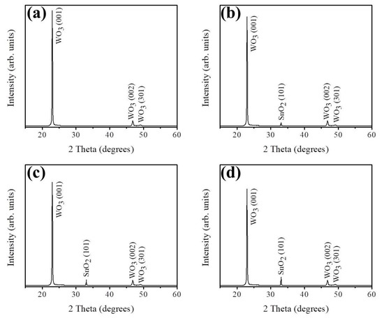
Figure 1.
X-ray diffraction (XRD) patterns of various nanorods: (a) WO3, (b) WS-1, (c) WS-2, and (d) WS-3.
SEM micrographs and the corresponding high magnification images of as-synthesized WO3 nanorods and various WO3–SnO2 composite nanorods are shown in Figure 2. The micrographs of the WO3 nanorods in Figure 2a show that the pristine WO3 nanorods feature obvious stripes on their surfaces extending along their growth directions and sharply structured heads. Moreover, the body is conically shaped. Figure 2b–d shows SEM images of WO3 nanorods sputter coated with SnO2 shell layers with various thicknesses. These WO3–SnO2 composite nanorods had a different morphology compared with those of the pristine WO3 nanorods. Notably, in Figure 2b, the WS-1 composite nanorods had a polycrystalline structure on the surfaces of the WO3 nanorods. Further increasing the SnO2 sputtering duration, from Figure 2c to Figure 2d, the morphology of the sputter-coated SnO2 shell layer gradually changed from tiny particle-feature-coverage layer to the coverage layer consisting of large crystal agglomerates. Notably, the shape of the top region of the composite nanorods in Figure 2d also changed from the original conical pileup to a cylindrical shape and all nanorods took on uniform cylindrical shapes. The SEM images showed that the surface morphology of the WO3–SnO2 composite nanorods varied with the sputtering duration of the SnO2. The roughening of the SnO2 coverage layer of the composite nanorods with prolonged sputtering duration was clearly demonstrated herein. The similar phenomenon has also been demonstrated in the ZnO–ZnS composite nanorod system synthesized by sputter-assisted coating of the ZnS shell layer on ZnO nanorods with different sputtering durations [18].
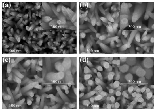
Figure 2.
Scanning electron microscopy (SEM) images of various nanorods: (a) WO3, (b) WS-1, (c) WS-2, and (d) WS-3. The corresponding high magnification images are shown in the insets of the figures.
The detailed morphology, the SnO2 coverage thickness, and the elemental distribution of various WO3–SnO2 composite nanorods (WS-1, WS-2, and WS-3) were further examined by TEM. Figure 3a shows a low magnification WS-1 nanorod. The composite nanorod exhibited a conical pileup morphology. The coverage layer consisted of tiny particle crystals and the thickness of the coverage layer was estimated to be approximately 13 nm at the top region of the nanorod. Figure 3b,c shows the high-resolution TEM (HRTEM) images of the WS-1 composite nanorod taken from the local interfacial regions of WO3/SnO2. The lattice fringes with a spacing of 0.39 nm in the inside region of the composite nanorods were assigned to the interplanar distance of hexagonal WO3 (001). In addition, the lattice fringes with a spacing of approximately 0.26 nm in the outside region of the composite nanorods were attributed to the interplanar distance of tetragonal SnO2 (101). Figure 3d demonstrates the Sn, W, and O elemental mapping images of the WS-1 composite nanorod. The W element was located inside the composite nanorod, revealing the position of the WO3 rod template. The Sn element spatially enclosed the whole rod body, demonstrating a homogeneous coverage of the SnO2 on the WO3 nanorods through sputtering SnO2 deposition. Similarly in the cross-sectional EDS line-scanning profiles (Figure 3d), the Sn and O signals were mainly distributed through the whole composite nanorod and the marked W signal was confined to the inner region of the composite nanorod, indicating that the composite nanorod consisted of a WO3 core and a SnO2 shell coverage layer.
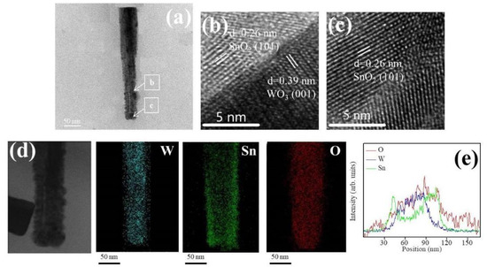
Figure 3.
(a) Low magnification transmission electron microscopy (TEM) image of a WS-1 nanorod. (b,c) High-resolution TEM (HRTEM) images of the nanorod taken from different regions. (d) W, Sn, and O elemental mapping images of the nanorod. (e) Elemental line-scanning profiles across the nanorod.
Figure 4a shows a low magnification TEM image of the WS-2 nanorod. Similar to the WS-1 nanorod shown in Figure 3a, the SnO2 coverage layer of the WS-2 still consisted of tiny SnO2 crystals. The SnO2 coverage layer, however, was denser and the crystal size of the SnO2 was larger than that in WS-1. The morphology of the WS-2 composite nanorod was more cylindrically shaped. The SnO2 coverage thickness at the top region of the composite nanorod was evaluated to be approximately 25 nm. Figure 4b,c shows the HRTEM images of the composite nanorods taken from the interfacial regions. The analysis the lattice fringes confirmed the crystal structures of the SnO2 coverage layer and WO3 nanorod. Furthermore, in Figure 4d, the Sn, W, and O elemental mapping images of the WS-2 composite nanorod revealed the Sn and O elements to be homogeneously distributed over the whole composite nanorod. The W element was confined in the inner regions of the composite nanorod. The EDS line-scanning profiles across the composite nanorod in Figure 4e supported the elemental mapping analysis results that the composite nanorods demonstrated a good WO3–SnO2 core–shell structure. Figure 5a shows a low magnification image of the WS-3 composite nanorod. The morphology of the WS-3 nanorod took on a fully cylindrical shape after the SnO3 sputtering deposition for 30 min. The crystal size of the SnO2 coverage layer of the WS-3 nanorod was substantially increased through the prolonged sputtering duration of SnO2 in comparison with those of the WS-1 and WS-2 nanorods. Moreover, these large SnO2 crystals or aggregates resulted in a rugged surface morphology of the WS-3 nanorods. The SnO2 coverage layer thickness at the top region of the composite nanorod was approximately 34 nm. The arrangements of local lattice fringes of the SnO2 coverage layer and of the WO3 core were also characterized in the HRTEM images (Figure 5b,c). Figure 5d,e demonstrates the homogeneous surface coverage of the Sn element through the whole WO3 nanorod. Notably, the intensity of the Sn signal in the EDS line-scanning profiles of various WO3–SnO2 composite nanorods increased with SnO2 sputtering duration as exhibited in the corresponding EDS spectra profiles, revealing an increased thickness of the SnO2 coverage layers on the composite nanorods. The TEM results herein revealed a good coverage of the sputter-deposited SnO2 thin films on the surface of the WO3 nanorods. A schematic summary of the morphology changes of the WO3–SnO2 composite nanorods prepared with various sputtering durations of SnO2 based on the TEM analysis results are also shown in Figure 5f.
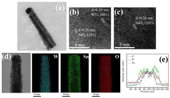
Figure 4.
(a) Low magnification TEM image of a WS-2 nanorod. (b,c) HRTEM images of the nanorod taken from different regions. (d) W, Sn, and O elemental mapping images of the nanorod. (e) Energy-dispersive X-ray spectroscopy (EDS) line-scanning profiles across the nanorod.
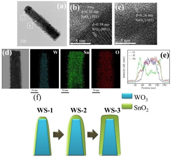
Figure 5.
(a) Low magnification TEM image of a WS-3 nanorod. (b,c) HRTEM images of the nanorod taken from different regions. (d) W, Sn, and O elemental mapping images of the nanorod. (e) EDS line-scanning profiles across the nanorod. (f) Schematics of the WS-1, WS-2, and WS-3 nanorods.
The peak intensity of W4f core-level doublets originating from the WO3 nanorods decreased and the peak intensity of the Sn 3d core-level doublets of the sputtered SnO2 coverage layers increased with the increase of the sputtering duration of SnO2 in Figure 6a,b. This reveals that the variation of the SnO2 shell layer thickness on the composite nanorods is controlled by the change in the sputtering duration of the SnO2 thin films. Figure 6a displays the W4f7/2 and W4f5/2 peaks centered at 35.9 and 37.9 eV, respectively, for the WO3 nanorods coated with various thicknesses of SnO2 thin films. The Gaussian deconvolution results of the W4f spectra of the various composite nanorods illustrated the contributions corresponding to the W5+ and W6+ states in the WO3. The main peaks centered at 35.9 and 37.9 eV correspond to W6+ binding states; moreover, the weaker intensity and lower binding energies for the subpeaks centered at 35.2 and 36.5 eV correspond to W5+ binding states. Figure 6b displays XPS Sn3d spectra of various WO3–SnO2 composite nanorods. A correspondence Sn3d5/2 peak centered at 487.1 eV and a Sn3d3/2 peak centered at approximately 495.4 eV were observed. The binding energy difference between the Sn3d5/2 and Sn3d3/2 corresponded to the chemical binding component of Sn4+ in the SnO2 [15,17]. The O1s XPS spectra of various composite nanorods in Figure 6c demonstrated three subcomponents. The component with a binding energy of approximately 529.8 eV is assigned to the tungsten oxide that formed the W–O bonds [19]. The second component with a binding energy of 530.5 eV is assigned to the tin oxide that formed the strong Sn–O bonds [15,17], and the small degree of oxygen vacancies and/or oxygen species chemisorbed from the ambient air were demonstrated in the component centered at approximately 531.9 eV.
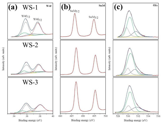
Figure 6.
High resolution X-ray photoelectron spectroscopy (XPS) spectra of various WO3–SnO2 composite nanorods: (a) W4f core-level doublet, (b) Sn3d core-level doublet, and (c) O1s peak.
Figure 7a–c demonstrates the variation of the temperature-dependent gas-sensing responses of the pristine WO3 nanorods, a 50 nm thick SnO2 film, and various WO3–SnO2 composite nanorods upon exposure to 100 ppm acetone vapor. The optimum operating temperature of the composite nanorods is lower than that of the WO3 nanorods and SnO2 thin film, in which they exhibited an optimal operating temperature of 325 °C. Previously, Zhang et al. showed that the La2O3-decorated SnO2 gas sensors feature a 2-fold higher gas-sensing performance improvement at 250 °C, which is lower than the optimum operating temperature of pristine SnO2 of 300 °C [20]. A decreased operating temperature of the oxide semiconductor through a heterostructure structure has also been shown in the ZnO–SnO2 system [21]. The optimal operating temperature for acetone gas-sensing examinations of various WO3–SnO2 composite nanorods was chosen to be 300 °C for this study.
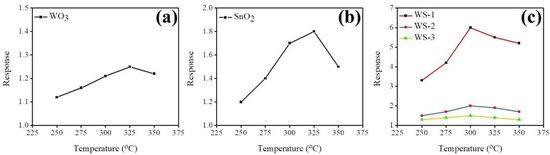
Figure 7.
Temperature-dependent gas-sensing responses for the gas sensors on exposure to 100 ppm acetone vapor at operating temperatures ranging from 250 to 350 °C: (a) WO3 nanorods, (b) SnO2 thin film, (c) various composite nanorods: WS-1 (red line), WS-2 (blue line), and WS-3 (yellow line).
Figure 8a–d shows the dynamic acetone gas-sensing response of pristine WO3 nanorods and various WO3–SnO3 nanorods upon exposure to various acetone vapor concentrations. The acetone gas-sensing responses of gas sensors made from various nanorods increased with the acetone vapor concentration, revealing that an increased number of acetone molecule numbers interacted with the absorbed oxygen species on the surfaces of the nanorods [15]. A plot of the acetone gas-sensing response vs. acetone vapor concentration is shown in Figure 8e. The acetone gas-sensing response of the pristine WO3 nanorods on exposure to 100–1000 ppm acetone vapor ranged from 1.25 to 1.35. The smooth and distinct dynamic response curves on exposure to various acetone vapor concentrations are demonstrated for the WO3 nanorods in Figure 8a, revealing that the WO3 nanorods are responding to acetone vapor; however, the response values are not high enough for practical use. By contrast, in Figure 8e, the WO3 nanorods coated with various thicknesses of SnO2 coverage layers exhibit an improved acetone gas-sensing capability compared with the pristine WO3 nanorods. The highest level of enhancement in acetone gas-sensing response was observed for the WS-1 nanorods. Their responses ranged from 6.3 to 12.1 upon exposure to 100 to 1000 ppm acetone vapor, respectively. An approximately 5-fold increase in the acetone gas-sensing response upon exposure to 100 ppm acetone vapor was observed for WO3 nanorods coated with 13 nm thick SnO2 films. Notably, thicker SnO2 coatings on the WO3 nanorods did not further enhance the acetone gas-sensing response of the composite nanorods. The acetone gas-sensing response decreases with SnO2 layer thickness as shown in Figure 8e. The optimal coating thickness of the SnO2 thin layer is approximately 13 nm for the WO3–SnO2 composite nanorod system herein. The response and recovery times for the gas sensors made from various nanorod samples are defined as the duration required to drop the 90% resistance on exposure to the target gas and that to increase 90% resistance with the removal of the target gas. The response times for the pristine WO3 nanorods exposed to 100–1000 ppm acetone vapor concentrations ranged from 8 to 17 s, whereas recovery times ranged from 33 to 58 s in the same acetone vapor concentration range. By contrast, the response times for the sensors made from the WS-2 and WS-3 composite nanorods ranged from 6 to 16 s and 20 to 32 s, respectively. The recovery times of the WS-2 and WS-3 composite nanorods were 38–83 s and 35–100 s in the acetone concentration range of 100–1000 ppm, respectively. Substantially increased response and recovery times were observed for the composite nanorods with the thickest SnO2 coverage layer. Notably, the response times and recovery times for the WS-1 composite nanorods in the same test acetone vapor concentration range ranged between 3–13 s and 28–51 s, respectively. The slightly improved response and recovery speeds together with the substantial enhancement in gas-sensing responses revealed an improved acetone gas-sensing performance of the WO3–SnO2 composite nanorods with an optimal SnO2 thin layer thickness of approximately 13 nm. Figure 8f displays cyclic acetone gas-sensing tests for the WS-1 composite nanorods exposed to 500 ppm acetone vapor. Steady gas-sensing activity under five test cycles was observed, confirming that WS-1 nanorods were reproducible and stable for detecting acetone vapor. Figure 8g shows the gas-sensing selectivity of CH3COCH3, H2, and NH3 gases with concentrations of 100 and 10 ppm for NO2 gas for the WS-1 composite nanorods. The WS-1 composite nanorods exhibited the best gas-sensing response toward acetone vapor among the various target gases. Table 1 summarizes the acetone gas-sensing responses of the WO3-based composites operating at the temperature range of 280–400 °C [22,23,24,25,26,27]. In comparison, the WS-1 composite nanorods presented the best acetone vapor detection performance among various reported works.
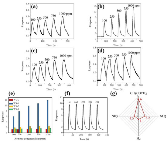
Figure 8.
Dynamic gas-sensing response–recovery curves of various nanorods upon exposure to different acetone vapor concentrations (100 to 1000 ppm): (a) WO3, (b) WS-1, (c) WS-2, and (d) WS-3 nanorods. (e) Gas-sensing response values vs. acetone vapor concentration for various nanorods. (f) Cyclic gas-sensing response curves for the WS-1 nanorods exposed to 500 ppm acetone vapor. (g) Gas-sensing selectivity of the WS-1 nanorods exposed to 100 ppm of CH3COCH3, NH3, and H2, and 5 ppm of NO2.

Table 1.
Summary of the acetone gas-sensing performances of various WO3-based composites operating in the temperature range of 280–400 °C [22,23,24,25,26,27]. N/A, Not available.
The acetone gas-sensing mechanism of WO3–SnO2 composite nanorods with an optimum thickness of SnO2 layer is illustrated in Figure 9. In our assessment of the gas-sensing mechanism, we follow the approach outlined in reference [28]. When thin SnO2 coverage layers are sputtered onto the surfaces of the WO3 nanorods, an interfacial depletion layer forms as a WO3/SnO2 heterojunction develops. According to the band alignment structure of the WO3/SnO2 in Figure 9a [29,30], an electron depletion layer initially forms on the WO3 side. Upon exposure of the WO3–SnO2 composite nanorods to ambient air, oxygen molecules remove surface electrons from the composite nanorods, thus forming adsorbed negatively charged oxygen species (Figure 9b). In this way, the sputter-coated SnO2 thin layers in the composite nanorods become partially depleted at some degrees under the sensor operating conditions. Notably, the extent of this depletion is highly dependent on the sensor operating temperature. The thickness of the surface depletion layer of the SnO2 at 327 °C in ambient air has been shown to be approximately 21 nm [31]. In ZnO–SnO2 core–shell nanowires, it has been proposed that the SnO2 shell layers with a thickness of 15–20 nm was fully depleted in the range of sensor operating temperatures of 200–400 °C [32]. The complete depletion of the SnO2 shell layer significantly affects the variation of the electron depletion layer width at the ZnO/SnO2 heterointerface during gas exposure, thus leading to a substantially enhanced gas-sensing performance [30]. In the current work, the extraction of surface electrons widened the thickness of the interfacial depletion layer and thus increased the interfacial potential barrier. In this way, the width of the electron conduction path through the single crystalline WO3 nanorods is reduced and the resistance of the composite nanorods is increased (Figure 9b). When acetone vapor is introduced into the test chamber, the interaction between the reducing acetone vapor and the adsorbed oxygen species of the surfaces of the composite nanorods can be expressed as follows [33]:
CH3COCH3 (gas) + 8O−ads → 3CO2 + 3H2O + 8e−.
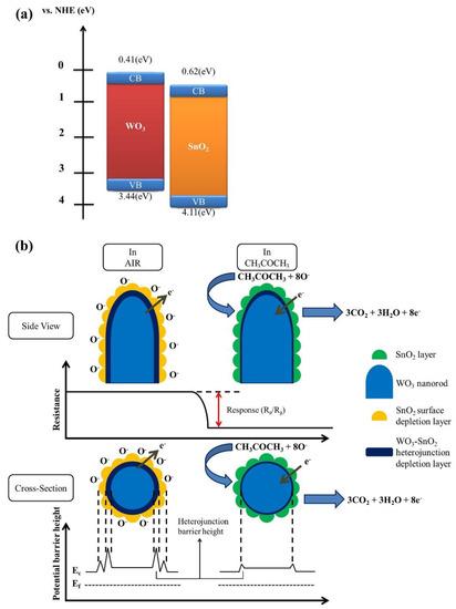
Figure 9.
(a) The conduction band-edge and valence band-edge positions of the WO3 and SnO2. (b) Schematics of possible gas-sensing mechanism of WS-1 nanorods on exposure to acetone vapor.
The release of free electrons from the adsorbed surface oxygen species eliminates the surface depletion regions in the SnO2 coverage layers and further narrows the size of interfacial depletion regions, thus causing the substantial drop in resistance of the composite nanorods. The marked resistance variation of the composite nanorods before and after introducing acetone vapor results in a distinct gas-sensing response of the composite nanorods upon exposure to acetone vapor. The efficiency of this process is critically dependent on the thickness of the SnO2 coverage layers. Our work suggests that in WO3–SnO2 composite nanorods this optimum thickness is close to 13 nm. In its order of magnitude, this value agrees with the results of previous investigations into core–shell SnO2–ZnO nanowires [34] and SnO2–ZnO nanofibers [35]. It appears that in all cases a substantial improvement in gas response is obtained when the thickness of the coverage layers is close to the respective Debye length.
4. Conclusions
WO3–SnO2 composite nanorods were synthesized by sputter coating a SnO2 coverage layer onto the surfaces of WO3 nanorods. The sputtering duration of SnO2 was varied to control the SnO2 coverage layer thickness on the WO3 nanorods in the range of 13–34 nm. Crystalline WO3–SnO2 composite nanorods were formed. Moreover, the evolution of the microstructure of the SnO2 coverage layers was characterized as a function of their thickness. Thicker SnO2 coverage layers exhibited larger surface crystals or aggregates. The acetone gas-sensing tests revealed that WO3–SnO2 composite nanorods with a 13 nm thick SnO2 coverage layer exhibited the best gas-sensing responses among the various composite nanorods. An optimum match of the SnO2 coverage layer thickness with the Debye length inside the coverage layers at the optimum operating temperature range is likely to account for the observed superior acetone gas-sensing responses of the WS-1 composite nanorods.
Author Contributions
Methodology, Y.C.; Formal analysis, Y.C.; Writing—original draft preparation, Y.-C.L.; Supervision, Y.-C.L.; Writing—review and editing, Y.-C.L.
Funding
This research was funded by the Ministry of Science and Technology of Taiwan, Grant No. MOST 105-2628-E-019-001-MY3.
Conflicts of Interest
The authors declare no conflict of interest.
References
- Zhao, S.; Shen, Y.; Zhou, P.; Li, G.; Han, C.; Wei, D.; Zhong, X.; Zhang, Y.; Ao, Y. Influence of synthesis conditions on microstructure and NO2 sensing properties of WO3 porous films synthesized by non-hydrolytic sol-gel method. Nanomaterials 2019, 9, 8. [Google Scholar] [CrossRef] [PubMed]
- Liang, Y.C.; Chang, C.W. Preparation of orthorhombic WO3 thin films and their crystal quality-dependent dye photodegradation ability. Coatings 2019, 9, 90. [Google Scholar] [CrossRef]
- Zhang, G.; Lu, K.; Zhang, X.; Yuan, W.; Ning, H.; Tao, R.; Liu, X.; Yao, R.; Peng, J. Enhanced transmittance modulation of SiO2-doped crystalline WO3 films prepared from a polyethylene oxide (PEO) template. Coatings 2018, 8, 228. [Google Scholar] [CrossRef]
- Liang, Y.C.; Chao, Y. Crystal phase content-dependent functionality of dual phase SnO2-WO3 nanocomposite films via cosputtering crystal growth. RSC Adv. 2019, 9, 6482–6493. [Google Scholar] [CrossRef]
- Wu, C.-S. Hydrothermal fabrication of WO3 hierarchical architectures: Structure, Growth and Response. Nanomaterials 2015, 5, 1250–1255. [Google Scholar] [CrossRef] [PubMed]
- Xue, D.; Wang, J.; Wang, Y.; Sun, G.; Cao, J.; Bala, H.; Zhang, Z. Enhanced methane sensing properties of WO3 nanosheets with dominant exposed (200) facet via loading of SnO2 nanoparticles. Nanomaterials 2019, 9, 351. [Google Scholar] [CrossRef] [PubMed]
- Liang, Y.C.; Xu, N.C. Synthesis of TiO2-ZnS nanocomposites via sacrificial template sulfidation and their ethanol gas-sensing performance. RSC Adv. 2018, 8, 22437–22446. [Google Scholar] [CrossRef]
- Liang, Y.C.; Xu, N.C.; Wang, C.C.; Wei, D.H. Fabrication of nanosized island-like CdO crystallites-decorated TiO2 rod nanocomposites via a combinational methodology and their low-concentration NO2 gas-sensing behavior. Materials 2017, 10, 778. [Google Scholar] [CrossRef] [PubMed]
- Liang, Y.C.; Lin, T.Y.; Lee, C.M. Crystal growth and shell layer crystal-feature-dependent sensing and photoactivity performance of zinc oxide-indium oxide core-shell nanorod heterostructures. CrystEngComm 2015, 17, 7948–7955. [Google Scholar] [CrossRef]
- Khan, M.E.; Khan, M.M.; Cho, M.H. Fabrication of WO3 nanorods on graphene nanosheets for improved visible light-induced photocapacitive and photocatalytic performance. RSC Adv. 2016, 6, 20824–20833. [Google Scholar] [CrossRef]
- Zhang, J.; Lu, H.; Liu, C.; Chen, C.; Xin, X. Porous NiO-WO3 heterojunction nanofibers fabricated by electrospinning with enhanced gas sensing properties. RSC Adv. 2017, 7, 40499–40509. [Google Scholar] [CrossRef]
- Wang, B.; Man, W.; Yu, H.; Li, Y.; Zheng, F. Fabrication of Mo-doped WO3 nanorod arrays on FTO substrate with enhanced electrochromic properties. Materials 2018, 11, 1627. [Google Scholar] [CrossRef] [PubMed]
- Yin, L.; Chen, D.; Feng, M.; Ge, L.; Yang, D.; Song, Z.; Fan, B.; Zhang, R.; Shao, G. Hierarchical Fe2O3@WO3 nanostructures with ultrahigh specific surface areas: Microwaveassisted synthesis and enhanced H2S-sensing performance. RSC Adv. 2015, 5, 328–337. [Google Scholar] [CrossRef]
- Zhao, Y.; Li, Y.; Ren, X.; Gao, F.; Zhao, H. The effect of Eu doping on microstructure, morphology and methanal-sensing performance of highly ordered SnO2 nanorods array. Nanomaterials 2017, 7, 410. [Google Scholar] [CrossRef] [PubMed]
- Liang, Y.C.; Lee, C.M.; Lo, Y.J. Reducing gas-sensing performance of Ce-doped SnO2 thin films through a cosputtering method. RSC Adv. 2017, 7, 4724–4734. [Google Scholar] [CrossRef]
- Wan, W.; Li, Y.; Ren, X.; Zhao, Y.; Gao, F.; Zhao, H. 2D SnO2 nanosheets: Synthesis, characterization, structures, and excellent sensing performance to ethylene glycol. Nanomaterials 2018, 8, 112. [Google Scholar] [CrossRef]
- Liang, Y.C.; Lo, Y.J. High-temperature solid-state reaction induced structure modifications and associated photoactivity and gas-sensing performance of binary oxide one-dimensional composite system. RSC Adv. 2017, 7, 29428–29439. [Google Scholar] [CrossRef]
- Liang, Y.C.; Lo, Y.R.; Wang, C.C.; Xu, N.C. Shell layer thickness-dependent photocatalytic activity of sputtering synthesized hexagonally structured ZnO-ZnS composite nanorods. Materials 2018, 11, 87. [Google Scholar] [CrossRef]
- Liang, Y.C.; Chang, C.W. Improvement of ethanol gas-sensing responses of ZnO-WO3 composite nanorods through annealing induced local phase transformation. Nanomaterials 2019, 9, 669. [Google Scholar] [CrossRef]
- Zhang, G.; Zhang, S.; Yang, L.; Zou, Z.; Zeng, D.; Xie, C. La2O3-sensitized SnO2 nanocrystalline porous film gas sensors and sensing mechanism toward formaldehyde. Sens. Actuators B 2013, 188, 137–146. [Google Scholar] [CrossRef]
- Ma, X.; Song, H.; Guan, C. Enhanced ethanol sensing properties of ZnO-doped porous SnO2 hollow nanospheres. Sens. Actuators B 2013, 188, 193–199. [Google Scholar] [CrossRef]
- Zhao, X.; Ji, H.; Jia, Q.; Wang, M. A nanoscale Co3O4-WO3 p-n junction sensor with enhanced acetone responsivity. J. Mater. Sci. Mater. Electron. 2015, 26, 8217–8223. [Google Scholar] [CrossRef]
- Choi, S.; Bonyani, M.; Sun, G.J.; Lee, J.K.; Hyun, S.K.; Lee, C. Cr2O3 nanoparticle-functionalized WO3 nanorods for ethanol gas sensors. Appl. Surf. Sci. 2018, 432, 241–249. [Google Scholar] [CrossRef]
- Choi, S.; Lee, J.K.; Lee, W.S.; Lee, C.; Lee, W.I. Acetone sensing of multi-networked WO3-NiO core-shell nanorod sensors. J. Korean Phys. Soc. 2017, 71, 487–493. [Google Scholar] [CrossRef]
- Dien, N.D. ZnO Microrods surface-decorated by WO3 nanorods for enhancing NH3 gas sensing performance. J. Sci. Technol. 2016, 54, 151–159. [Google Scholar] [CrossRef]
- Kim, N.H.; Choi, S.J.; Kim, S.J.; Cho, H.J.; Jang, J.S.; Koo, W.T.; Kim, M.; Kim, I.D. Highly sensitive and selective acetone sensing performance of WO3 nanofibers functionalized by Rh2O3 nanoparticles. Sens. Actuators B 2016, 224, 185–192. [Google Scholar] [CrossRef]
- Li, F.; Gao, X.; Wang, R.; Zhang, T. Design of WO3-SnO2 core-shell nanofibers and their enhanced gas sensing performance based on different work function. Appl. Surf. Sci. 2018, 442, 30–37. [Google Scholar] [CrossRef]
- Sun, P.; Cai, Y.; Du, S.; Xu, X.; You, L.; Ma, J.; Liu, F.; Liang, X.; Sun, Y.; Lu, G. Hierarchical α-Fe2O3/SnO2 semiconductor composites: Hydrothermal synthesis and gas sensing properties. Sens. Actuators B 2013, 182, 336–343. [Google Scholar] [CrossRef]
- Aslam, I.; Cao, C.; Tanveer, M.; Khan, W.S.; Tahir, M.; Abid, M.; Idrees, F.; Butt, F.K.; Ali, Z.; Mahmood, N. The synergistic effect between WO3 and g-C3N4 towards efficient visible-light-driven photocatalytic performance. New J. Chem. 2014, 38, 5462–5469. [Google Scholar] [CrossRef]
- Baek, J.H.; Kim, B.J.; Han, G.S.; Hwang, S.W.; Kim, D.R.; Cho, I.S.; Jung, H.S. BiVO4/WO3/SnO2 double-heterojunction photoanode with enhanced charge separation and visible-transparency for bias-free solar water-splitting with a perovskite solar cell. ACS Appl. Mater. Interfaces 2017, 9, 1479–1487. [Google Scholar] [CrossRef]
- Barsan, N.; Weimar, U. Conduction model of metal oxide gas sensors. J. Electroceram. 2001, 7, 143–167. [Google Scholar] [CrossRef]
- Hwang, I.S.; Kim, S.J.; Choi, J.K.; Choi, J.; Ji, H.; Kim, G.T.; Cao, G.; Lee, J.H. Synthesis and gas sensing characteristics of highly crystalline ZnO-SnO2 core-shell nanowires. Sens. Actuators B 2010, 148, 595–600. [Google Scholar] [CrossRef]
- Yin, M.; Yao, Y.; Fan, H.; Liu, S. WO3-SnO2 nanosheet composites: Hydrothermal synthesis and gas sensing mechanism. J. Alloys Compd. 2018, 736, 322–331. [Google Scholar] [CrossRef]
- Choi, S.W.; Katoch, A.; Sun, G.J.; Kim, J.H.; Kim, S.H.; Kim, S.S. Dual functional sensing mechanism in SnO2-ZnO core-shell nanowires. ACS Appl. Mater. Interfaces 2014, 6, 8281–8287. [Google Scholar] [CrossRef] [PubMed]
- Katoch, A.; Choi, S.W.; Sun, G.J.; Kim, S.S. An approach to detecting a reducing gas by radial modulation of electron-depleted shells in core-shell nanofibers. J. Mater. Chem. A 2013, 1, 13588–13596. [Google Scholar] [CrossRef]
© 2019 by the authors. Licensee MDPI, Basel, Switzerland. This article is an open access article distributed under the terms and conditions of the Creative Commons Attribution (CC BY) license (http://creativecommons.org/licenses/by/4.0/).