Tuning the Doping Ratio and Phase Transition Temperature of VO2 Thin Film by Dual-Target Co-Sputtering


 ,
, 
Abstract
:1. Introduction
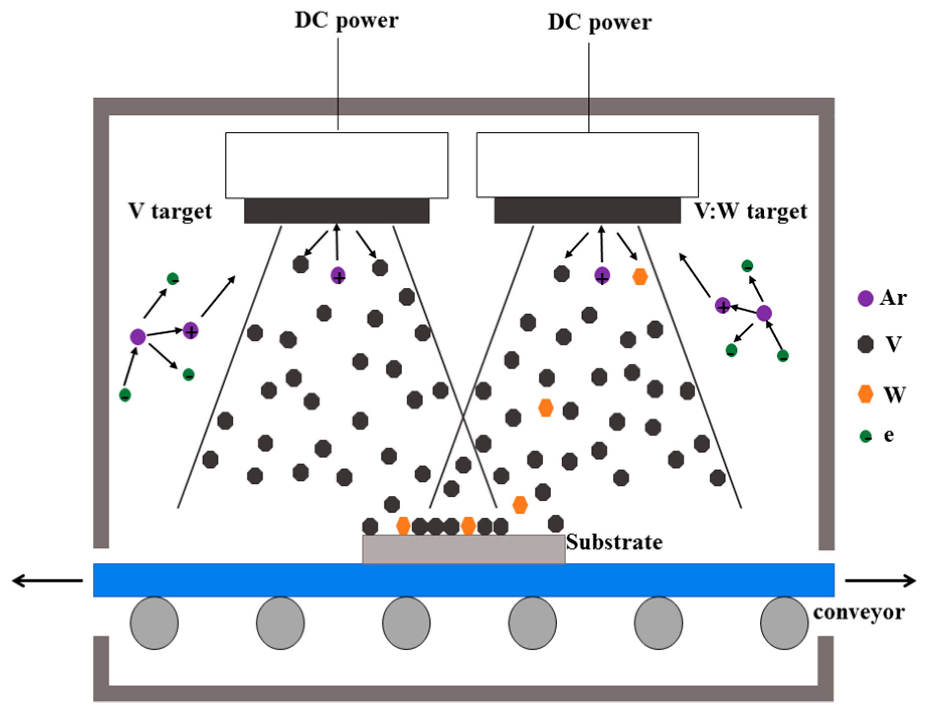
2. Experimental Procedure
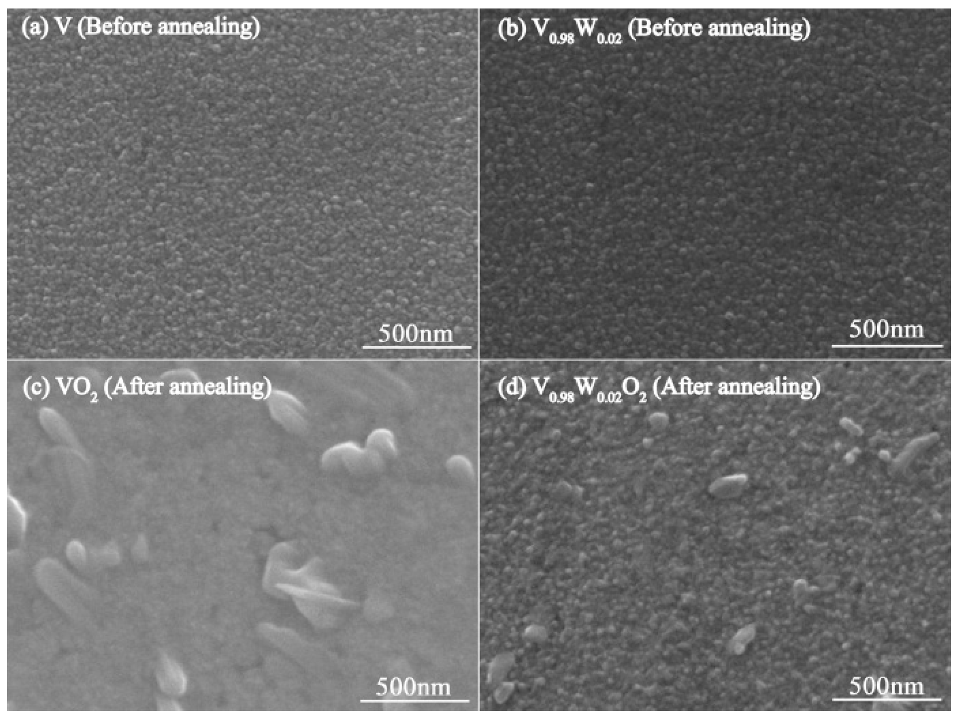
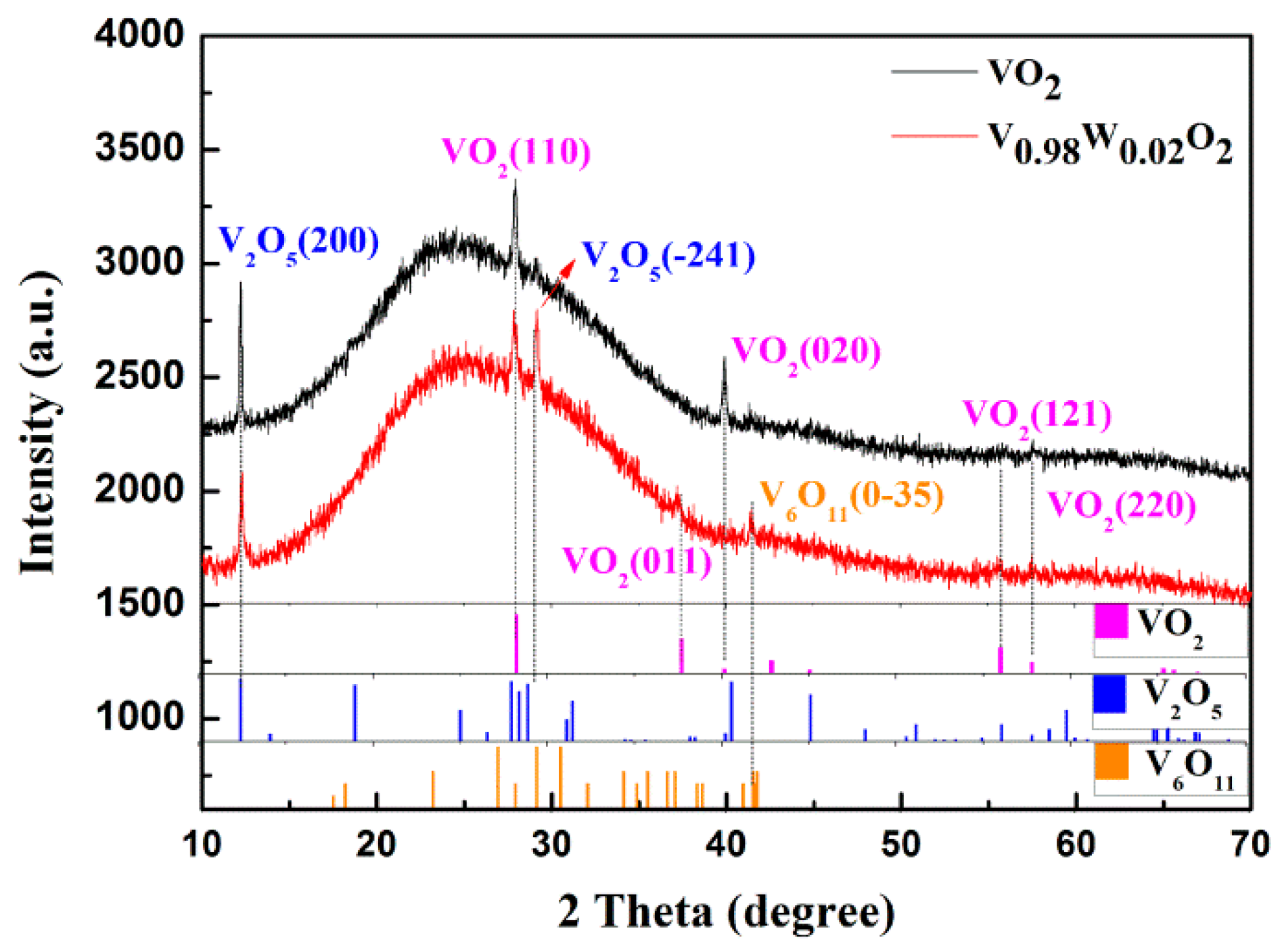
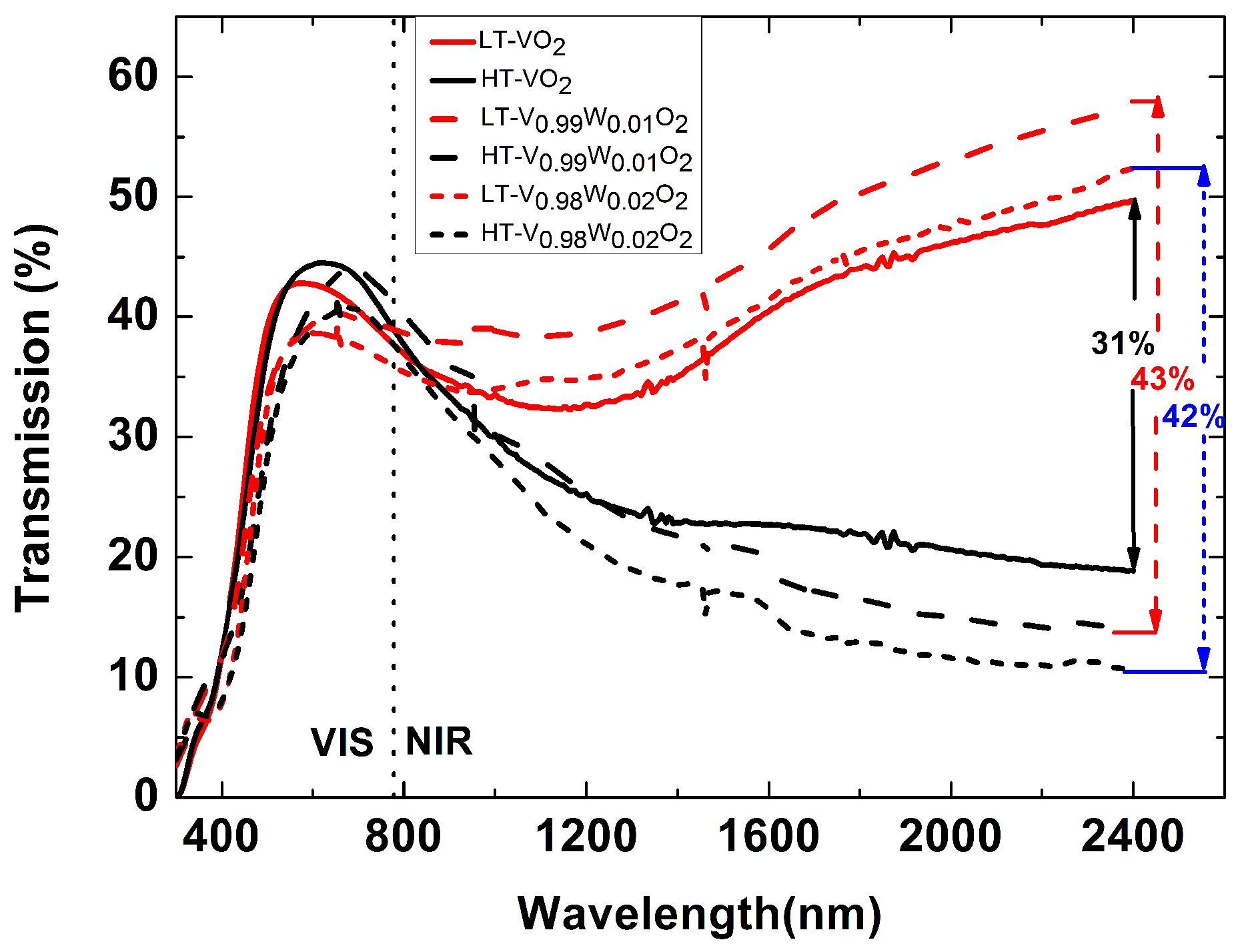
3. Results and Discussion
4. Conclusions
Author Contributions
Funding
Conflicts of Interest
References
- Morin, F.J. Oxides which show a metal-to-insulator transition at the neel temperature. Phys. Rev. Lett. 1959, 3, 34–36. [Google Scholar] [CrossRef]
- Chen, X.Q.; Yi, X.J.; Yang, Y.; Li, Y. A new CMOS readout circuit for VO2-based uncooled focal polane arrays. Int. J. Infrared Millim. Waves 2006, 27, 1281–1291. [Google Scholar] [CrossRef]
- Chen, S.H.; Ma, H.; Yi, X.J.; Xiong, T.; Wang, H.C.; Ke, C.J. Smart VO2 thin film for protection of sensitive infrared detectors from strong laser radiation. Sens. Actuator A-Phys. 2004, 115, 28–31. [Google Scholar] [CrossRef]
- Jin, P.; Xu, G.; Tazawa, M.; Yoshimura, K. Design, formation and characterization of a novel multifunctional window with VO2 and TiO2 coatings. Appl. Phys. A-Mater. Sci. Process. 2003, 77, 455–459. [Google Scholar] [CrossRef]
- Kana, J.B.K.; Ndjaka, J.M.; Ateba, P.O.; Ngom, B.D.; Manyala, N.; Nemraoui, O.; Beye, A.C.; Maaza, M. Thermochromic VO2 thin films synthesized by rf-inverted cylindrical magnetron sputtering. Appl. Surf. Sci. 2008, 254, 3959–3963. [Google Scholar] [CrossRef]
- Brassard, D.; Fourmaux, S.; Jean-Jacques, M.; Kieffer, J.C.; El Khakani, M.A. Grain size effect on the semiconductor-metal phase transition characteristics of magnetron-sputtered VO2 thin films. Appl. Phys. Lett. 2005, 87, 051910. [Google Scholar] [CrossRef]
- Sohn, J.I.; Joo, H.J.; Kim, K.S.; Yang, H.W.; Jang, A.R.; Ahn, D.; Lee, H.H.; Cha, S.; Kang, D.J.; Kim, J.M.; et al. Stress-induced domain dynamics and phase transitions in epitaxially grown VO2 nanowires. Nanotechnology 2012, 23, 205707. [Google Scholar] [CrossRef] [PubMed]
- Crunteanu, A.; Givernaud, J.; Leroy, J.; Mardivirin, D.; Champeaux, C.; Orlianges, J.C.; Catherinot, A.; Blondy, P. Voltage- and current-activated metal-insulator transition in VO2-based electrical switches: A lifetime operation analysis. Sci. Technol. Adv. Mater. 2010, 11, 065002. [Google Scholar] [CrossRef]
- Mun, B.S.; Yoon, J.; Mo, S.K.; Chen, K.; Tamura, N.; Dejoie, C.; Kunz, M.; Liu, Z.; Park, C.; Moon, K.; et al. Role of joule heating effect and bulk-surface phases in voltage-driven metal-insulator transition in VO2 crystal. Appl. Phys. Lett. 2013, 103, 061902. [Google Scholar] [CrossRef]
- Jiming, B.; Lihua, M.; Shukuo, Z. Structural and optical properties of VO2 film grown on sapphire substrate by pulsed laser deposition. Adv. Mater. Res. 2014, 912, 325–328. [Google Scholar] [CrossRef]
- Chen, S.; Dong, C.Z.; Zhang, L.F.; Yu, Z.M. Annealing effects on W-doped VO2 thin films prepared from magnetron sputtering. In Materials Processing Technology Ii, Pts 1–4; Zhao, L.C., Wang, H., Xiao, C.F., Eds.; Trans Tech Publications Ltd.: Durnten-Zurich, Switzerland, 2012; Volume 538–541, pp. 101–104. [Google Scholar]
- Liu, X.X.; Wang, S.W.; Chen, F.L.; Yu, L.M.; Chen, X.S. Tuning phase transition temperature of VO2 thin films by annealing atmosphere. J. Phys. D-Appl. Phys. 2015, 48, 265104. [Google Scholar] [CrossRef]
- Liu, D.Q.; Cheng, H.F.; Xing, X.; Zhang, C.Y.; Zheng, W.W. Thermochromic properties of W-doped VO2 thin films deposited by aqueous sol-gel method for adaptive infrared stealth application. Infrared Phys. Technol. 2016, 77, 339–343. [Google Scholar] [CrossRef]
- Zhang, Y.F.; Li, W.; Fan, M.J.; Zhang, F.F.; Zhang, J.C.; Liu, X.H.; Zhang, H.N.; Huang, C.; Li, H.B. Preparation of W- and Mo-doped VO2(M) by ethanol reduction of peroxovanadium complexes and their phase transition and optical switching properties. J. Alloy. Compd. 2012, 544, 30–36. [Google Scholar] [CrossRef]
- Du, J.; Gao, Y.F.; Luo, H.J.; Zhang, Z.T.; Kang, L.T.; Chen, Z. Formation and metal-to-insulator transition properties of VO2-ZrV2O7 composite films by polymer-assisted deposition. Sol. Energy Mater. Sol. Cells 2011, 95, 1604–1609. [Google Scholar] [CrossRef]
- Miyazaki, K.; Shibuya, K.; Suzuki, M.; Wado, H.; Sawa, A. Correlation between thermal hysteresis width and broadening of metal-insulator transition in Cr- and Nb-doped VO2 films. Jpn. J. Appl. Phys. 2014, 53, 071102. [Google Scholar] [CrossRef]
- Jin, P.; Tazawa, M.; Ikeyama, M.; Tanemura, S.; Macak, K.; Wang, X.; Olafsson, S.; Helmersson, U. Growth and characterization of epitaxial films of tungsten-doped vanadium oxides on sapphire (110) by reactive magnetron sputtering. J. Vac. Sci. Technol. A-Vac. Surf. Films 1999, 17, 1817–1821. [Google Scholar] [CrossRef]
- Soltani, M.; Chaker, M.; Haddad, E.; Kruzelecky, R.V.; Margot, J. Effects of Ti–W codoping on the optical and electrical switching of vanadium dioxide thin films grown by a reactive pulsed laser deposition. Appl. Phys. Lett. 2004, 85, 1958–1960. [Google Scholar] [CrossRef]
- Li, J.H.; Yuan, N.Y.; Xie, T.B.; Dan, D.D. Preparation of polycrystalline V0.97W0.03O2 thin films with ultra high TCR at room temperature. Acta Phys. Sin. 2007, 56, 1790–1795. [Google Scholar]
- Wang, S.W.; Chen, X.S.; Lu, W.; Wang, L.; Wu, Y.G.; Wang, Z.S. Integrated optical filter arrays fabricated by using the combinatorial etching technique. Opt. Lett. 2006, 31, 332–334. [Google Scholar] [CrossRef]
- Wang, S.W.; Liu, D.; Lin, B.; Chen, X.; Lu, W. 16 × 1 integrated filter array in the MIR region prepared by using a combinatorial etching technique. Appl. Phys. B-Lasers Opt. 2006, 82, 637–641. [Google Scholar] [CrossRef]
- Wang, S.W.; Li, M.; Xia, C.S.; Wang, H.Q.; Chen, X.S.; Lu, W. 128 channels of integrated filter array rapidly fabricated by using the combinatorial deposition technique. Appl. Phys. B-Lasers Opt. 2007, 88, 281–284. [Google Scholar] [CrossRef]
- Liu, X.X.; Wang, S.W.; Xia, H.; Zhang, X.T.; Ji, R.N.; Li, T.X.; Lu, W. Interference-aided spectrum-fitting method for accurate film thickness determination. Chin. Opt. Lett. 2016, 14, 081203. [Google Scholar] [CrossRef]
- Liu, X.X.; Ji, R.N.; Zhang, Y.; Li, H.G.; Wang, S.W. Annealing process and mechanism of glass based VO2 film from V oxidation in pure oxygen atmosphere. Opt. Quantum Electron. 2016, 48, 453. [Google Scholar] [CrossRef]
- Li, H.Q.; He, X.X.; Liu, T.; Nie, Z.H.; Lv, X.Q. Modulus and Internal Friction of W-Doped VO2 Thin Films. Appl. Mech. Mater. 2011, 130, 3343–3346. [Google Scholar] [CrossRef]
- Li, J.; Liu, C.-Y.; Mao, L.-J. The character of W-doped one-dimensional VO2 (M). J. Solid State Chem. 2009, 182, 2835–2839. [Google Scholar] [CrossRef]
- Piccirillo, C.; Binions, R.; Parkin, I.P. Synthesis and characterisation of W-doped VO2 by Aerosol Assisted Chemical Vapour Deposition. Thin Solid Films 2008, 516, 1992–1997. [Google Scholar] [CrossRef]

© 2019 by the authors. Licensee MDPI, Basel, Switzerland. This article is an open access article distributed under the terms and conditions of the Creative Commons Attribution (CC BY) license (http://creativecommons.org/licenses/by/4.0/).
Share and Cite
Chen, X.; Wu, M.; Liu, X.; Wang, D.; Liu, F.; Chen, Y.; Yi, F.; Huang, W.; Wang, S. Tuning the Doping Ratio and Phase Transition Temperature of VO2 Thin Film by Dual-Target Co-Sputtering. Nanomaterials 2019, 9, 834. https://doi.org/10.3390/nano9060834
Chen X, Wu M, Liu X, Wang D, Liu F, Chen Y, Yi F, Huang W, Wang S. Tuning the Doping Ratio and Phase Transition Temperature of VO2 Thin Film by Dual-Target Co-Sputtering. Nanomaterials. 2019; 9(6):834. https://doi.org/10.3390/nano9060834
Chicago/Turabian StyleChen, Xu, Mingfei Wu, Xingxing Liu, Ding Wang, Feng Liu, Yuwei Chen, Fei Yi, Wanxia Huang, and Shaowei Wang. 2019. "Tuning the Doping Ratio and Phase Transition Temperature of VO2 Thin Film by Dual-Target Co-Sputtering" Nanomaterials 9, no. 6: 834. https://doi.org/10.3390/nano9060834
APA StyleChen, X., Wu, M., Liu, X., Wang, D., Liu, F., Chen, Y., Yi, F., Huang, W., & Wang, S. (2019). Tuning the Doping Ratio and Phase Transition Temperature of VO2 Thin Film by Dual-Target Co-Sputtering. Nanomaterials, 9(6), 834. https://doi.org/10.3390/nano9060834