1. Introduction
Three-dimensional (3D) topological insulators (TIs) are a new class of materials that have attracted great interests in both theoretic [
1,
2,
3,
4] and experimental [
5,
6,
7] researches in recent years. In 3D TIs, there is an insulating gap in bulk states accompanying with robust metallic topological surface states (TSSs) arising from band inversion caused by strong spin–orbit coupling. These TSSs are protected by time-reversal symmetry (TRS) and consist of spin-momentum locked massless Dirac electrons. The most widely studied 3D TIs are A
2B
3-family including Bi
2Se
3, Bi
2Te
3, and Sb
2Te
3, which have larger band gaps as well as simpler surface structure (only single Dirac cone in their surface states) compared to the first experimentally observed 3D TI, the Bi
1−xSb
x alloy.
The doping of TIs is one of the promising ways to realize new types of devices and new classes of materials. For instance, induced superconductivity (SC) has been reported in Bi
2Se
3 with intercalating Cu or Sr atoms between neighboring quintuple layers [
8,
9,
10,
11,
12]. A theoretical study predicts that topological SC in doped topological insulators may be suitable for hosting Majorana fermions and have potential application in fault-tolerant topological quantum computing [
13]. For Bi
2Se
3 with intercalating Cu dopant, it was showed that the spin-polarized TSSs are preserved at the Fermi level while SC occurs in bulk regime, suggesting that superconducting Cu
xBi
2Se
3 may be suitable for trapping non-Abelian Majorana fermions [
14]. Equally interesting, quantum anomalous Hall (QAH) effect is expected to emerge in magnetically doped TIs due to the broken TRS [
15]. In fact, quantization of the Hall resistance of h/e
2 at zero field, a signature of QAH effect, was observed in Cr-doped (Bi,Sb)
2Te
3 thin films at temperature below 30mK [
16,
17]. The electrical and magnetic properties of TIs are also found to be sensitive to extrinsic chemical doping. It has been reported that Fe-substituted Bi
2Se
3 favors ferromagnetic interactions while antiferromagnetic interactions dominates in Cr-substituted Bi
2Se
3 [
18]. N. H. Jo et al. reported that the incorporation of Fe in bulk single crystal of Bi
2-xFe
xTe
3 with
x ranging from 0.08 to 0.3 leads to the change of the conduction type from n-type to p-type at
x = 0.3 (equivalent to 6% for the atomic concentration of Fe) [
19].
In 2014, our group discovered a novel two-dimensional (2D) SC at the interface of a Bi
2Te
3/FeTe heterostructure [
20]. Another independent study also observed a superconducting energy gap by spin-polarized scanning tunneling spectroscopy for one unit cell FeTe on Bi
2Te
3 substrate with
TC = 6 K [
21]. However, the underlying mechanism of this SC has not been understood so far. In this study, we fabricated a Bi
2Te
3:Fe sample with varying Fe concentration along the growth direction so as to study if a certain Fe doping concentration in Bi
2Te
3 could make it superconducting, which is based on the thought that the observed interfacial SC at the Bi
2Te
3/FeTe heterostructure may be caused by forming a superconducting Bi
2Te
3:Fe layer at the interface of the heterostructure at a certain doping level due to Fe diffusion. Interestingly, this sample indeed shows a superconducting transition at its resistance vs temperature curve. We address the cause of the observed SC and the formation of two types of Fe-based nanostructures found in this sample through an unexpected formation mechanism, attributed to the non-thermal equilibrium growth mode of the molecular beam epitaxy (MBE) technique. It is worth pointing out that usually nanostructures can be fabricated using either top-down or bottom-up approach. In this study, we present a special approach, based on
in situ heavy doping, to synthesizing nanostructures under the condition that the dopant element is strongly reactive with an element in the host matrix.
Our studies reveal that in situ doping of a highly reactive dopant using a non-thermal equilibrium growth technique could result in unexpected phases of nanostructures embedded in the host matrix, providing a new path for forming new nanostructured materials.
2. Materials and Methods
All samples studied in this work are fabricated in a VG-V80H MBE system (VG SCIENTIFIC, Waltham, MA, USA) equipped with in situ reflection high-energy electron diffraction facility. High purity Bi2Te3 compound source (GoodFellow, Huntingdon, UK; 99.999%) together with an Fe elemental source (GoodFellow, Huntingdon, UK; 99.95%) were used for the MBE growth. The key sample for our studies is a multilayer sample. Prior to its growth, a semi-insulating GaAs (111)B substrate (AXT Inc., Fremont, CA, USA) was first thermally heated to 580 °C to remove the passivation oxide. Then a pure Bi2Te3 thin film of thickness ~15 nm was grown, followed by the growth of a set of Bi2Te3 layers with gradually increasing Fe concentration by opening the shutter of the Fe effusion cell with its cell temperature varying from a starting value of 880 °C to an ending value of 1150 °C with a step of 30 °C; the nominal thickness of each layer is estimated to be ~10 nm. During the whole growth process, the temperatures of the substrate and the Bi2Te3 effusion cell were kept at 235 °C and 420 °C, respectively. We have made an estimation of the highest apparent doping concentration of Fe in this sample with a result of ~8% in atomic concentration, which was estimated based on the growth rates of a pure Bi2Te3 layer and a pure FeTe layer grown with the Fe cell temperature at 1150 °C assuming the sticking coefficient of Fe in both the growth of Bi2Te3:Fe and FeTe is equal to one. A comparison group of samples containing a pure 24 nm Bi2Te3 layer grown on a GaAs (111)B (AXT Inc., Fremont, CA, USA) substrate and a pure 150 nm FeTe layer grown on a ZnSe(~70 nm)/GaAs(100) substrate (AXT Inc., Fremont, CA, USA) were also fabricated. ZnSe compound source (Alfa Aesar, Ward Hill, MA, USA; 99.999%), Te elemental source (ESPI Metals, Ashland, OR, USA; 99.999%), Bi2Te3 and Fe sources were used for the growth of these samples.
Each sample was cut into long strips (with dimension ~2 × 6 mm2), and conventional four-point electric contacts were made on the surface using silver paint as the contact material for conducting transport measurements. Their electrical and magnetotransport properties were measured in a Quantum Design physical property measurement system (PPMS, model 6000, Quantum Design, Inc., San Diego, CA, USA). High-resolution X-ray diffraction (HRXRD) measurements were conducted by PANalytical multipurpose diffractometer with an X’celerator detector (PANalytical X’Pert Pro, Malvern, UK) for composition and crystalline phase characterizations. Cross-sectional high-resolution transmission electron microscopy (HRTEM) images were taken in a JEOL 2010F TEM (JEOL Ltd., Tokyo, Japan) with acceleration voltage of 200 kV in conventional TEM mode. Plan view scanning electron microscopy (SEM) images were taken in a JEOL JSM-6390 SEM (JEOL Ltd., Tokyo, Japan). Both TEM and SEM systems are equipped with energy dispersive X-ray spectroscopy (EDS). The scanning TEM (STEM) studies were performed using an aberration-corrected JEOL JEM-ARM200F TEM (JEOL Ltd., Tokyo, Japan) working under dark-field, which provides both EDS mapping and corresponding TEM imaging.
3. Results and Discussion
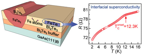
First, we measured the electrical and magnetotransport properties of the Bi
2Te
3:Fe thin film and a pure Bi
2Te
3 thin film aiming to investigate the effects of Fe doping.
Figure 1a shows the temperature dependence of the in-plane resistance of both samples. It is well known that a defect-free intrinsic Bi
2Te
3 thin film with thickness > 1 nm has gapped bulk states and the Fermi level lies in the energy gap (very close to the valence band) [
4], thus it is expected to show a narrow-gap semiconductor behavior at low temperature. The Bi
2Te
3 thin film studied in this work, however, shows a metallic behavior instead as displayed in
Figure 1a. This behavior is believed to be attributed to Te vacancies generated in the synthesizing process, which shifts the Fermi level into the conduction band. Generation of Te vacancies in Bi
2Te
3 is common in MBE growth [
22] and other growth techniques [
6,
23]. As can be seen in
Figure 1a, the
R vs
T curve of the Bi
2Te
3:Fe thin film overall displays a metallic behavior, however, a sudden drop in resistance occurs at temperature ~12.3 K at zero magnetic field.
Figure 1b shows the temperature-dependent resistance of the Bi
2Te
3:Fe thin film in the temperature range from 2 to 16 K at the presence of external magnetic field up to 12 T, revealing that the onset of the drop of resistance (marked by arrows) shifts to lower temperature as the external magnetic field increases.
Figure 1c shows the temperature-dependent resistance of the pure Bi
2Te
3 thin film under magnetic fields of the same range; however, apart from seeing a moderate positive magnetoresistance effect, no sign of a superconducting transition can be seen. The above experimental observations indicate that our Bi
2Te
3:Fe thin film enjoys a SC feature attributed to the incorporation of Fe dopants.
However, neither previous theoretical [
24] nor experimental [
18,
19] studies on Fe uniformly doped Bi
2Te
3 samples predict or observe SC. Moreover, it is not likely that the SC at ~12 K shown in our Bi
2Te
3:Fe sample comes from an ordinarily Fe-doped Bi
2Te
3 thin film because the induced SC in A
2B
3-type topological insulators usually has a much lower
TC. For example, it was reported that bulk SC can be achieved with
TC of 2.28 K in Tl
0.6Bi
2Te
3 [
25], 2.9 K in Sr-intercalated Bi
2Se
3 [
10,
11,
12], and up to 3.8 K in Cu
xBi
2Se
3 [
8,
9,
14]. In fact, the detected SC in our Bi
2Te
3:Fe sample with
TC of ~12 K is reminiscent of the 2D SC in the Bi
2Te
3/FeTe bilayer heterostructure discovered by our group previously [
20], of which the maximum
TC of a series of Bi
2Te
3/FeTe heterostructure sample with different Bi
2Te
3 thicknesses is also ~12 K. In order to find out the source of the observed SC, we conducted detailed structural and chemical analysis on the Bi
2Te
3:Fe sample.
Figure 2a displays a plan view SEM image of the surface of the Bi
2Te
3:Fe thin film within an area of 11 × 15 µm
2. It can be seen that some nanorods are embedded in the thin film with length around 1 μm and width around 200 nm. These nanorods are aligned in three directions (marked by the dash lines) and the angle between two neighboring directions is 120°. Another type of nanostructure is the islands that are favorably formed on the nanorods. To obtain the chemical composition of the nanorods and the islands, line-scanning EDS was performed across these two nanostructures as shown in
Figure 2b in which the solid line indicates the trace of the focused electron beam. The corresponding EDS spectrum is depicted in the lower row of
Figure 2b. It clearly shows that the X-ray signal generated by Bi atoms drops sharply and the opposite trends occur for those of Fe and Te atoms when the electron beam enters the nanorods. On the other hand, the chemical composition of the island seems to be the same as that of the neighboring Bi
2Te
3 region, though the signals of Bi and Te at the island site are contributed by both the island and underlying Bi
2Te
3 layer, however, as the thickness of the island is about half of the underlying Bi
2Te
3 layer (this will be addressed later), this claim should still be valid. Thus one can conclude that the nanorods likely consist of Fe and Te atoms mainly, however, it is not reliable to determine their chemical ratio by the EDS technique since it is well known that EDS is just a semiquantitative technique. HRXRD and HRTEM were then performed with the aim to achieve more quantitative structural and chemical analysis for the Bi
2Te
3:Fe thin film.
The top part of
Figure 3 plots the HRXRD profile of the Bi
2Te
3:Fe thin film in symmetric 2
θ-ω scan mode using an X-ray beam with wavelength λ of 1.540598 Å generated from Cu K-α1. The composition of the Bi
2Te
3:Fe thin film was determined through a detailed study on this HRXRD profile. The lower part of
Figure 3 shows the powder diffraction files (PDFs) of the three crystalline materials contained in the thin film, where only the peaks oriented along the normal of the sample surface are extracted for clarity. As can be seen in
Figure 3, the two strongest peaks are the (111) and (222) peaks of the GaAs substrate, the next four strong peaks match well with the (0 0 6), (0 0 15), (0 0 18), and (0 0 21) peaks of Bi
2Te
3. From these four peaks we have calculated the corresponding lattice parameter in the z-direction to be
c = 30.45 Å, which indeed agrees well with the reported standard value of
c = 30.48 Å [
26]. The two peaks at 2
θ of 34.06° and 71.71° match quite well with the (020) and (040) peaks of an unexpected phase, FeTe
2. A careful inspection of
Figure 3 could also find the evidence of the existence of the four characteristic diffraction peaks of (001), (002), (003), and (004) of another unexpected phase—FeTe—though the (002) peak is buried in the GaAs (111) peak. In the following two paragraphs, the solid evidence, provided by HRTEM imaging studies, for the existence of FeTe
2 and FeTe phases in our Bi
2Te
3:Fe sample will be addressed.
Figure 4 displays the TEM images, fast Fourier-transform (FFT) patterns and relevant schematic lattice drawings for the nanostructures and thin film layer involved in the Bi
2Te
3:Fe sample.
Figure 4a shows the cross-sectional TEM image of a typical example of the nanorods shown in the SEM image in
Figure 2. As shown, it has a trapezoidal cross-section and its bottom surface reaches the top surface of the GaAs substrate.
Figure S1 in Supplementary Materials shows a cross-sectional TEM image of another typical nanorod that lands its root inside the Bi
2Te
3 layer. The reason why we could claim that this type of nanostructure in the film is the nanorods seen in the SEM image is that their width and number density in the TEM images match quite well with those derived from the SEM image. In the left of
Figure 4b, a finer HRTEM image of the nanorod shown in
Figure 4a is displayed and the FFT pattern of a region of the nanorod (marked by the square in
Figure 4b is shown in the right which displays a pattern match very well with a simulated diffraction pattern of FeTe
2 along [100] zone axis. The left of
Figure 4c shows the HRTEM image of a small region of the FeTe
2 nanorod, where the dominating lattice presents a layer of Te atoms within the same lattice plane. This figure also shows the measured lattice spacings of 6.2 Å and 5.3 Å, corresponding to the horizontal and vertical values, respectively, both agree well with the corresponding lattice spacings of an atomic lattice model of FeTe
2 shown in the upper right of
Figure 4c, where the highlighted four Te1 atoms correspond to one unit cell of the image shown in the left of
Figure 4c. At the lower right of
Figure 4c, the top view of the FeTe
2 lattice with its [010] direction pointing out of the page and along the c-axis of Bi2Te3, that is, normal to the sample surface, is shown. One can see that the upper two layers of Te atoms form a quasi-hexagonal shape with its lattice dimension enjoys a small lattice-mismatch of ~16% as compared with that of Bi
2Te
3 (001). We believe that this might be the reason why the FeTe
2 nanorods prefer to grow upward along its [010] direction because this quasi-hexagonal shape might have provided a relatively better lattice match with the hexagonal lattice arrangement of Bi
2Te
3 along its
c-axis than other possible growth directions. A related issue regarding the preferred three lateral growth directions of the FeTe
2 nanorods as shown in the SEM image of
Figure 2a, perhaps can be attributed to the well-known three-fold symmetry of the Bi
2Te
3 lattice planes perpendicular to its
c-axis [
4], which leads to the lateral growth of the FeTe
2 nanorods to select the corresponding three directions that enjoy the highest symmetry. As shown in
Figure 4a, an island with base width ~100 nm and height ~50 nm can be found located above the FeTe
2 nano-rod, which corresponds to one of the many islands seen in the SEM image shown in
Figure 2a. In
Figure S2 of the Supplementary Materials, we have provided evidence via its HRTEM images and EDS analysis to show that the islands are Bi
2Te
3 in composition and likely contain several grains with different orientations.
Among the HRTEM images of the Bi
2Te
3:Fe sample, we have found another type of nanostructures, which can only be found near the surface of the sample and its number density is much less than that of the FeTe
2 nanorods. In
Figure S3 of the Supplementary Materials, the EDS profile performed on this nanostructure indicates that it mainly consists of Fe and Te in composition.
Figure 4d shows the HRTEM image of this relatively rare nanostructure and its neighboring region. The left and right of
Figure 4e show a zoomed-in HRTEM image of
Figure 4d and its FFT patterns of this nanostructure and its neighboring region, respectively, with the top FFT pattern matches with the diffraction pattern expected from [010]-oriented FeTe and the bottom one matches with that of [
]-oriented Bi
2Te
3. The left of
Figure 4f shows an HRTEM image of the FeTe nanostructure at atomic scale, revealing the two orthogonal lattice parameters to be a = 3.6 Å and c = 6.1Å, which are in good agreement with the schematic drawing of a FeTe lattice viewed along the [100] direction [
27], which is displayed in the right of
Figure 4f, where the highlighted four Te(a) atoms correspond to one unit cell of the image shown in the left of
Figure 4f. In fact, the existence of such a FeTe nanostructure in the Bi
2Te
3:Fe sample as revealed via cross-sectional HRTEM studies echoes the detection of a FeTe phase in the HRXRD profile as shown in
Figure 3. Due to the time-consuming TEM sample preparation process and limited area of thin region in TEM sample, it is difficult to estimate a precise density of FeTe nanostructures. A plan view TEM sample was also examined; however, we could not observe the FeTe phase but could observe FeTe
2 nanorods, because FeTe lies under the sample surface. Thus it is not possible to tell the shape of the FeTe nanostructures, either, at the moment. A rough estimation is that the distance between two FeTe nanostructures formed near the sample surface is ~5 μm, and the length of FeTe nanostructures ranges from 100 to 400 nm. As for FeTe
2 nanorods, their surface density counted from SEM image is 24.7%. Assuming the surface density of FeTe
2 nanorods is a constant within the most top 3 nm layer, and taking the volume per each element in Bi
2Te
3 and FeTe
2 phases into consideration, we calculated the highest Fe atomic doping concentration at the top surface is 6.9%, which is close to the value of 8.0% that was estimated based on the growth rate.
Through the above detailed structural and chemical analysis of the various phases exist in the Bi
2Te
3: Fe sample, now it is clear that the observed SC at ~12 K as displayed in
Figure 1 can be attributed to the heterojunction formed by the FeTe nanostructure and its neighboring Bi
2Te
3 layer, because such a heterojunction has been demonstrated by us previously to enjoy SC with a critical temperature ~12 K if its Bi
2Te
3 component is thicker than 5 nm [
20]. The magnetic field dependences of the onset temperature of the detected drop of resistance for the Bi
2Te
3:Fe thin film, and a Bi
2Te
3(7 nm)/FeTe heterostructure is plotted in
Figure 1d, which indeed shows a similar trend. In
Figure S4 of the Supplementary Materials, we have provided further electrical and magnetotransport results, which provide further evidence that the observed SC in the Bi
2Te
3:Fe sample likely shares the same origin of the SC at the interface of a Bi
2Te
3/FeTe heterostructure.
In the following paragraph, we present a phenomenological model for the formation mechanisms of the three types of nanostructures, namely FeTe
2 nanorods, FeTe nanostructure, and Bi
2Te
3 islands, found in the Bi
2Te
3: Fe sample based on the findings presented above. We believe that the formation of the first two Fe-Te nanostructures are attributed to the strong reaction between the Fe atoms with the Te atoms either from the Bi
2Te
3 source flux or the Te lattice atoms in the as-grown Bi
2Te
3 layers. The fact that in the Bi
2Te
3:Fe sample, a 15-nm-thick pure buffer Bi
2Te
3 layer was first grown before the cosupplying of both Bi
2Te
3 and Fe fluxes, however, most of the FeTe
2 nanorods were found to reach the top surface of the GaAs substrate. This indicates that the strong reaction between Fe and Te atoms could even lead to the breaking of the bonds of Bi
2Te
3 to form a FeTe
2 phase. Since the Bi
2Te
3:Fe sample was grown with an increasing Fe flux, the FeTe
2 nanorods formed at some preferred seeds correspondingly grow in bigger size along the upward direction (normal to the sample surface), forming a trapezoidal cross-sectional shape as shown in
Figure 4a,b. However, the growth rate of FeTe
2 nanorods along the upward direction is slower than the growth rate of the neighboring Bi
2Te
3 layer, thus these nanorods appear to be dented as shown in the SEM image displayed in
Figure 2a. As the highest Fe flux was provided near the end of the growth, it provided the condition to form a Fe-Te compound with more rich in Fe composition as compared with the FeTe
2 nanorods, thus this explains why the early mentioned FeTe nanostructures could be formed near the surface of the sample. Since Bi
2Te
3 flux were also provided simultaneously together with the elemental Fe flux, Bi
2Te
3 islands are favored to form in the two ends of the dented FeTe
2 nanorods, where the kink edges provides the most favorable sites for them to sit in, attributed to the fundamental understanding based on surface energy minimization scheme.
Figure 5 is a flow chart illustrating the formation mechanisms described above.

 ,
, 


