Optimizing the Interface between Hole Transporting Material and Nanocomposite for Highly Efficient Perovskite Solar Cells


 ,
, 
Abstract
1. Introduction
2. Experimental Section
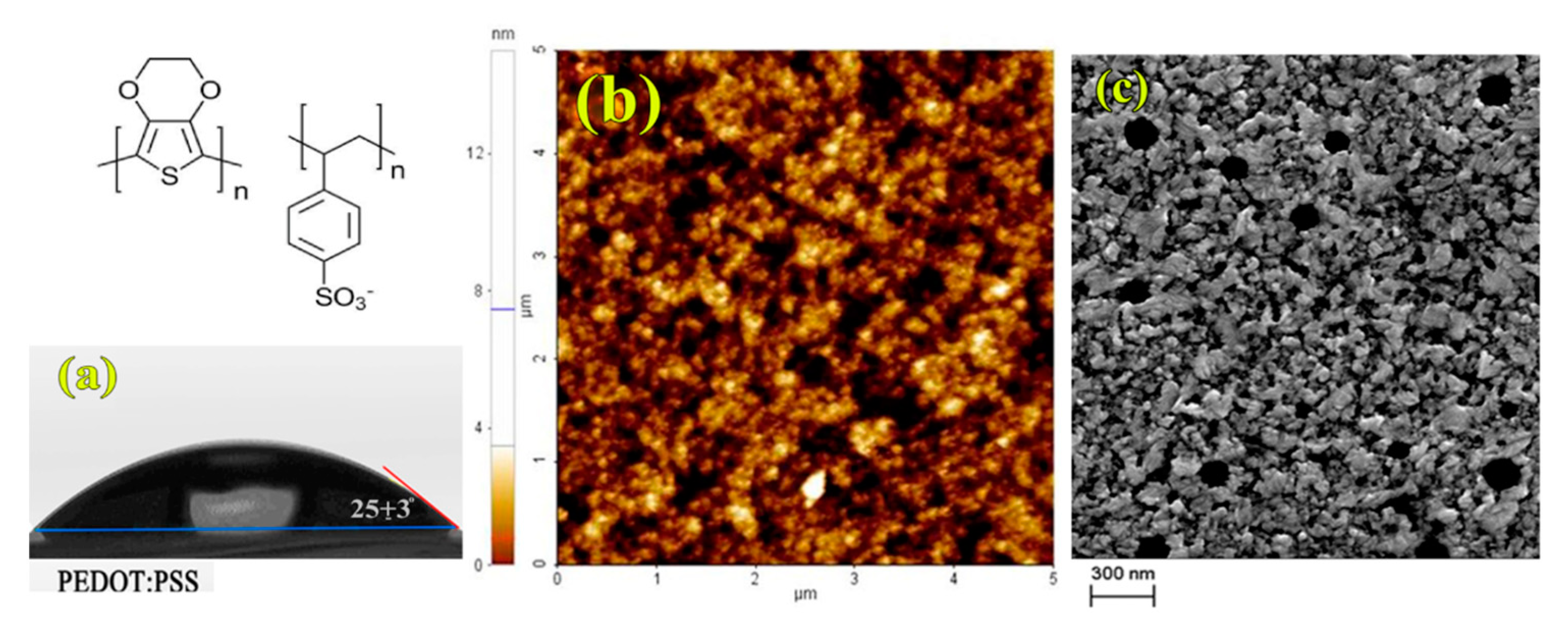
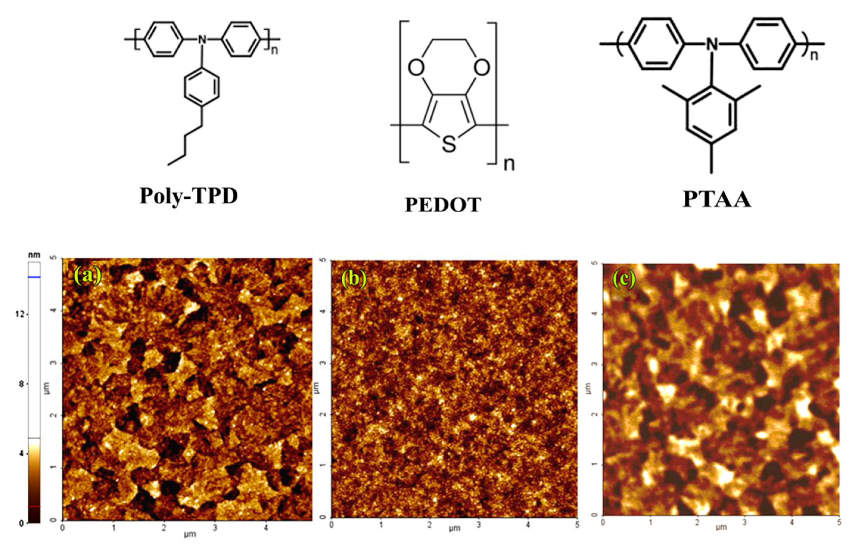
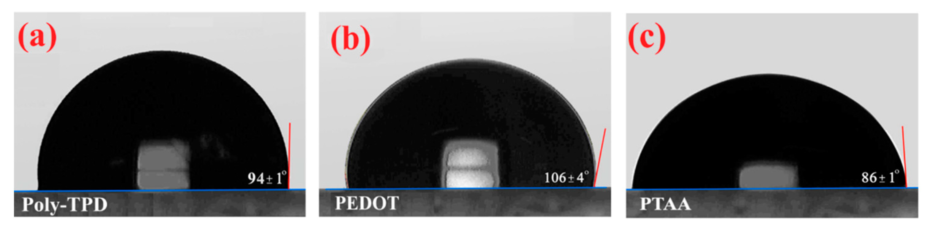
2.1. Materials
2.2. MAPI: Starch Based Solution Preparation
2.3. Oxygen Plasma Treatment
2.4. Characterization
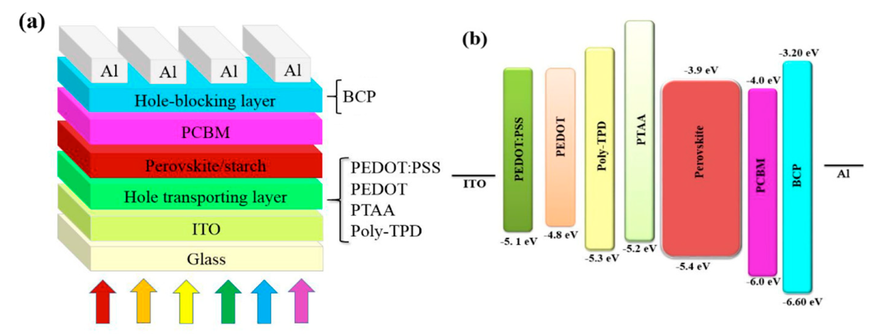
2.5. Device Fabrication and Characterization
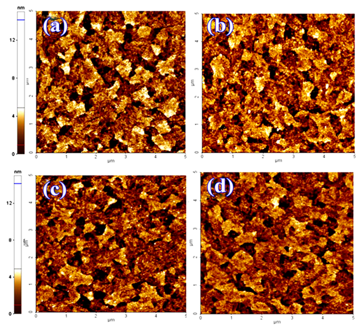
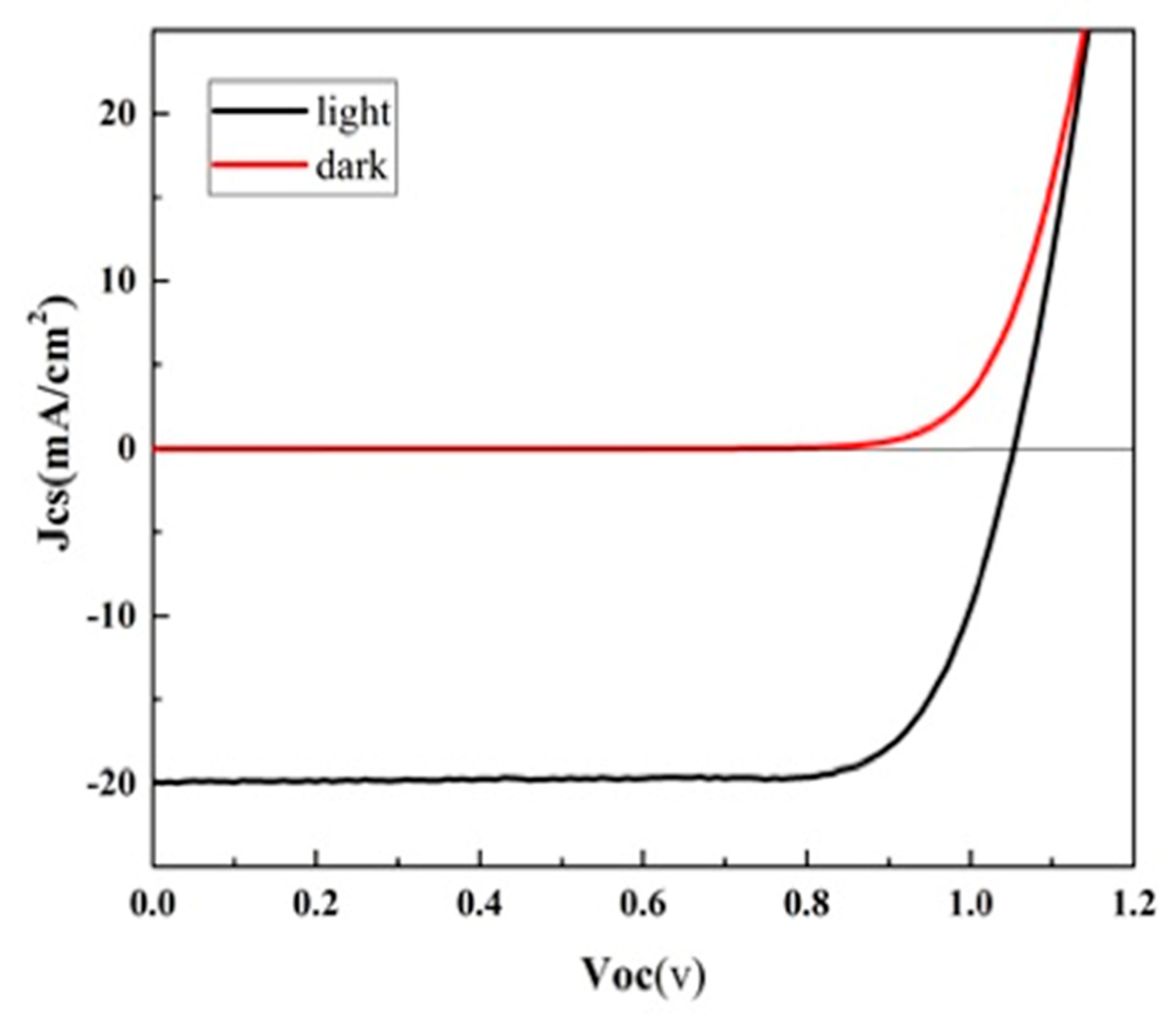
3. Results and Discussion
Inverted Perovskite Solar Cells Performance
4. Conclusions
Author Contributions
Funding
Conflicts of Interest
References
- Lee, M.M.; Teuscher, J.; Miyasaka, T.; Murakami, T.N.; Snaith, H.J. Efficient hybrid solar cells based on meso-superstructured organometal halide perovskites. Science 2012, 338, 643–647. [Google Scholar] [CrossRef]
- Chen, Y.; Zhang, L.; Zhang, Y.; Gao, H.; Yan, H. Large-area perovskite solar cells—A review of recent progress and issues. RSC Adv. 2018, 8, 10489–10508. [Google Scholar] [CrossRef]
- Tang, H.; He, S.; Peng, C. A short progress report on high-efficiency perovskite solar cells. Nanoscale Res. Lett. 2017, 12, 410. [Google Scholar] [CrossRef] [PubMed]
- Shi, Z.; Jayatissa, A. Perovskites-based solar cells: A review of recent progress, materials and processing methods. Materials 2018, 11, 729. [Google Scholar] [CrossRef] [PubMed]
- Jeyaraman, A.R.; Balasingam, S.K.; Lee, C.; Lee, H.; Balakrishnan, B.; Manickam, S.; Yi, M.; Kim, H.-J.; Nallathambi, K.S.; Jun, Y. Enhanced solar to electrical energy conversion of titania nanoparticles and nanotubes-based combined photoanodes for dye-sensitized solar cells. Mater. Lett. 2019, 243, 180–182. [Google Scholar] [CrossRef]
- Sarwar, S.; Ko, K.-W.; Han, J.; Han, C.-H.; Jun, Y.; Hong, S. Improved long-term stability of dye-sensitized solar cell by zeolite additive in electrolyte. Electrochim. Acta 2017, 245, 526–530. [Google Scholar] [CrossRef]
- Liu, Y.; Renna, L.A.; Bag, M.; Page, Z.A.; Kim, P.; Choi, J.; Emrick, T.; Venkataraman, D.; Russell, T.P. High efficiency tandem thin-perovskite/polymer solar cells with a graded recombination layer. ACS Appl. Mater. Interfaces 2016, 8, 7070–7076. [Google Scholar] [CrossRef]
- Sun, S.; Salim, T.; Mathews, N.; Duchamp, M.; Boothroyd, C.; Xing, G.; Sum, T.C.; Lam, Y.M. The origin of high efficiency in low-temperature solution-processable bilayer organometal halide hybrid solar cells. Energy Environ. Sci. 2014, 7, 399–407. [Google Scholar] [CrossRef]
- Miyata, A.; Mitioglu, A.; Plochocka, P.; Portugall, O.; Wang, J.T.-W.; Stranks, S.D.; Snaith, H.J.; Nicholas, R.J. Direct measurement of the exciton binding energy and effective masses for charge carriers in organic—Inorganic tri-halide perovskites. Nat. Phys. 2015, 11, 582. [Google Scholar] [CrossRef]
- Li, Y.; Ji, L.; Liu, R.; Zhang, C.; Mak, C.H.; Zou, X.; Shen, H.-H.; Leu, S.-Y.; Hsu, H.-Y. A review on morphology engineering for highly efficient and stable hybrid perovskite solar cells. J. Mater. Chem. A 2018, 6, 12842–12875. [Google Scholar] [CrossRef]
- Kojima, A.; Teshima, K.; Shirai, Y.; Miyasaka, T. Organometal halide perovskites as visible-light sensitizers for photovoltaic cells. J. Am. Chem. Soc. 2009, 131, 6050–6051. [Google Scholar] [CrossRef] [PubMed]
- Sahli, F.; Werner, J.; Kamino, B.A.; Bräuninger, M.; Monnard, R.; Paviet-Salomon, B.; Barraud, L.; Ding, L.; Leon, J.J.D.; Sacchetto, D. Fully textured monolithic perovskite/silicon tandem solar cells with 25.2% power conversion efficiency. Nat. Mater. 2018, 17, 820. [Google Scholar] [CrossRef] [PubMed]
- Cui, P.; Wei, D.; Ji, J.; Huang, H.; Jia, E.; Dou, S.; Wang, T.; Wang, W.; Li, M. Planar p–n homojunction perovskite solar cells with efficiency exceeding 21.3%. Nat. Energy 2019, 4, 150. [Google Scholar] [CrossRef]
- Li, W.; Liu, J.; Zhao, D. Mesoporous materials for energy conversion and storage devices. Nat. Rev. Mater. 2016, 1, 16023. [Google Scholar] [CrossRef]
- Trifiletti, V.; Manfredi, N.; Listorti, A.; Altamura, D.; Giannini, C.; Colella, S.; Gigli, G.; Rizzo, A. Engineering TiO2/Perovskite Planar Heterojunction for Hysteresis-Less Solar Cells. Adv. Mater. Interfaces 2016, 3, 1600493. [Google Scholar] [CrossRef]
- Saliba, M.; Correa-Baena, J.-P.; Wolff, C.M.; Stolterfoht, M.; Phung, N.; Albrecht, S.; Neher, D.; Abate, A. How to make over 20% efficient perovskite solar cells in regular (n–i–p) and inverted (p–i–n) architectures. Chem. Mater. 2018, 30, 4193–4201. [Google Scholar] [CrossRef]
- Liu, T.; Chen, K.; Hu, Q.; Zhu, R.; Gong, Q. Inverted perovskite solar cells: Progresses and perspectives. Adv. Energy Mater. 2016, 6, 1600457. [Google Scholar] [CrossRef]
- Reza, K.M.; Mabrouk, S.; Qiao, Q. A Review on Tailoring PEDOT: PSS Layer for Improved Performance of Perovskite Solar Cells. Proc. Nat. Res. Soc. 2018, 2, 02004. [Google Scholar] [CrossRef]
- Jhuo, H.-J.; Yeh, P.-N.; Liao, S.-H.; Li, Y.-L.; Sharma, S.; Chen, S.-A. Inverted perovskite solar cells with inserted cross-linked electron-blocking interlayers for performance enhancement. J. Mater. Chem. A 2015, 3, 9291–9297. [Google Scholar] [CrossRef]
- Wang, Q.; Bi, C.; Huang, J. Doped hole transport layer for efficiency enhancement in planar heterojunction organolead trihalide perovskite solar cells. Nano Energy 2015, 15, 275–280. [Google Scholar] [CrossRef]
- Lee, I.; Rolston, N.; Brunner, P.-L.; Dauskardt, R.H. Hole-transport layer molecular weight and doping effects on perovskite solar cell efficiency and mechanical behavior. ACS Appl. Mater. Interfaces 2019. [Google Scholar] [CrossRef] [PubMed]
- Tafazoli, S.; Timasi, N.; Nouri, E.; Mohammadi, M. The role of a vapor-assisted solution process on tailoring the chemical composition and morphology of mixed-halide perovskite solar cells. CrystEngComm 2018, 20, 4428–4435. [Google Scholar] [CrossRef]
- Genco, A.; Mariano, F.; Carallo, S.; Guerra, V.L.; Gambino, S.; Simeone, D.; Listorti, A.; Colella, S.; Gigli, G.; Mazzeo, M. Fully Vapor-Deposited Heterostructured Light-Emitting Diode Based on Organo-Metal Halide Perovskite. Adv. Electron. Mater. 2016, 2, 1500325. [Google Scholar] [CrossRef]
- Carnie, M.J.; Charbonneau, C.; Davies, M.L.; Troughton, J.; Watson, T.M.; Wojciechowski, K.; Snaith, H.; Worsley, D.A. A one-step low temperature processing route for organolead halide perovskite solar cells. Chem. Commun. 2013, 49, 7893–7895. [Google Scholar] [CrossRef] [PubMed]
- Safari, Z.; Zarandi, M.B.; Nateghi, M.R. Improved environmental stability of HTM free perovskite solar cells by a modified deposition route. Chem. Pap. 2019, 73, 2667–2678. [Google Scholar] [CrossRef]
- Bi, D.; Moon, S.-J.; Häggman, L.; Boschloo, G.; Yang, L.; Johansson, E.M.J.; Nazeeruddin, M.K.; Grätzel, M.; Hagfeldt, A. Using a two-step deposition technique to prepare perovskite (CH3NH3PbI3) for thin film solar cells based on ZrO2 and TiO2 mesostructures. RSC Adv. 2013, 3, 18762–18766. [Google Scholar] [CrossRef]
- Kajal, P.; Ghosh, K.; Powar, S. Manufacturing techniques of perovskite solar cells. In Applications of Solar Energy; Tyagi, H., Ed.; Springer Nature: Singapore, 2018; pp. 341–364. [Google Scholar]
- Chilvery, A.; Das, S.; Guggilla, P.; Brantley, C.; Sunda-Meya, A. A perspective on the recent progress in solution-processed methods for highly efficient perovskite solar cells. Sci. Technol. Adv. Mater. 2016, 17, 650–658. [Google Scholar] [CrossRef]
- Wang, F.; Bai, S.; Tress, W.; Hagfeldt, A.; Gao, F. Defects engineering for high-performance perovskite solar cells. npj Flex. Electron. 2018, 2, 22. [Google Scholar] [CrossRef]
- Kim, J.; Lee, S.-H.; Lee, J.H.; Hong, K.-H. The role of intrinsic defects in methylammonium lead iodide perovskite. J. Phys. Chem. Lett. 2014, 5, 1312–1317. [Google Scholar] [CrossRef]
- Uratani, H.; Yamashita, K. Charge carrier trapping at surface defects of perovskite solar cell absorbers: A first-principles study. J. Phys. Chem. Lett. 2017, 8, 742–746. [Google Scholar] [CrossRef]
- Colella, S.; Todaro, M.; Masi, S.; Listorti, A.; Altamura, D.; Caliandro, R.; Giannini, C.; Carignani, E.; Geppi, M.; Meggiolaro, D. Light-Induced Formation of Pb3+ Paramagnetic Species in Lead Halide Perovskites. ACS Energy Lett. 2018, 3, 1840–1847. [Google Scholar] [CrossRef]
- Kim, M.K.; Jeon, T.; Park, H.I.; Lee, J.M.; Nam, S.A.; Kim, S.O. Effective control of crystal grain size in CH3NH3PbI3 perovskite solar cells with a pseudohalide Pb(SCN)2 additive. CrystEngComm 2016, 18, 6090–6095. [Google Scholar] [CrossRef]
- Chang, C.-Y.; Chu, C.-Y.; Huang, Y.-C.; Huang, C.-W.; Chang, S.-Y.; Chen, C.-A.; Chao, C.-Y.; Su, W.-F. Tuning perovskite morphology by polymer additive for high efficiency solar cell. ACS Appl. Mater. Interfaces 2015, 7, 4955–4961. [Google Scholar] [CrossRef] [PubMed]
- Li, T.; Pan, Y.; Wang, Z.; Xia, Y.; Chen, Y.; Huang, W. Additive engineering for highly efficient organic—Inorganic halide perovskite solar cells: Recent advances and perspectives. J. Mater. Chem. A 2017, 5, 12602–12652. [Google Scholar] [CrossRef]
- Masi, S.; Aiello, F.; Listorti, A.; Balzano, F.; Altamura, D.; Giannini, C.; Caliandro, R.; Uccello-Barretta, G.; Rizzo, A.; Colella, S. Connecting the solution chemistry of PbI2 and MAI: A cyclodextrin-based supramolecular approach to the formation of hybrid halide perovskites. Chem. Sci. 2018, 9, 3200–3208. [Google Scholar] [CrossRef]
- Masi, S.; Rizzo, A.; Munir, R.; Listorti, A.; Giuri, A.; Esposito Corcione, C.; Treat, N.D.; Gigli, G.; Amassian, A.; Stingelin, N. Organic gelators as growth control agents for stable and reproducible hybrid perovskite-based solar cells. Adv. Energy Mater. 2017, 7, 1602600. [Google Scholar] [CrossRef]
- Mastria, R.; Colella, S.; Qualtieri, A.; Listorti, A.; Gigli, G.; Rizzo, A. Elucidating the effect of the lead iodide complexation degree behind the morphology and performance of perovskite solar cells. Nanoscale 2017, 9, 3889–3897. [Google Scholar] [CrossRef]
- Ko, Y.; Kim, Y.; Lee, C.; Kim, Y.; Jun, Y. Poly (methyl methacrylate) embedded perovskite films for improving solar cell performance. Synth. Metals 2019, 249, 47–51. [Google Scholar] [CrossRef]
- Masi, S.; Colella, S.; Listorti, A.; Roiati, V.; Liscio, A.; Palermo, V.; Rizzo, A.; Gigli, G. Growing perovskite into polymers for easy-processable optoelectronic devices. Sci. Rep. 2015, 5, 7725. [Google Scholar] [CrossRef]
- Giuri, A.; Saleh, E.; Listorti, A.; Colella, S.; Rizzo, A.; Tuck, C.; Esposito Corcione, C. Rheological Tunability of Perovskite Precursor Solutions: From Spin Coating to Inkjet Printing Process. Nanomaterials 2019, 9, 582. [Google Scholar] [CrossRef]
- Masi, S.; Rizzo, A.; Aiello, F.; Balzano, F.; Uccello-Barretta, G.; Listorti, A.; Gigli, G.; Colella, S. Multiscale morphology design of hybrid halide perovskites through a polymeric template. Nanoscale 2015, 7, 18956–18963. [Google Scholar] [CrossRef] [PubMed]
- Giuri, A.; Masi, S.; Listorti, A.; Gigli, G.; Colella, S.; Corcione, C.E.; Rizzo, A. Polymeric rheology modifier allows single-step coating of perovskite ink for highly efficient and stable solar cells. Nano Energy 2018, 54, 400–408. [Google Scholar] [CrossRef]
- Giuri, A.; Yuan, Z.; Miao, Y.; Wang, J.; Gao, F.; Sestu, N.; Saba, M.; Bongiovanni, G.; Colella, S.; Corcione, C.E. Ultra-Bright Near-Infrared Perovskite Light-Emitting Diodes with Reduced Efficiency Roll-off. Sci. Rep. 2018, 8, 15496. [Google Scholar] [CrossRef] [PubMed]
- Weber, S.A.; Hermes, I.M.; Turren-Cruz, S.-H.; Gort, C.; Bergmann, V.W.; Gilson, L.; Hagfeldt, A.; Graetzel, M.; Tress, W.; Berger, R. How the formation of interfacial charge causes hysteresis in perovskite solar cells. Energy Environ. Sci. 2018, 11, 2404–2413. [Google Scholar] [CrossRef]
- Bai, Y.; Meng, X.; Yang, S. Interface engineering for highly efficient and stable planar p-i-n perovskite solar cells. Adv. Energy Mater. 2018, 8. [Google Scholar] [CrossRef]
- Guerra, V.L.; Altamura, D.; Trifiletti, V.; Colella, S.; Listorti, A.; Giannuzzi, R.; Pellegrino, G.; Condorelli, G.G.; Giannini, C.; Gigli, G. Implications of TiO2 surface functionalization on polycrystalline mixed halide perovskite films and photovoltaic devices. J. Mater. Chem. A 2015, 3, 20811–20818. [Google Scholar] [CrossRef]
- Ponchai, J.; Kaewurai, P.; Boonthum, C.; Pinsuwan, K.; Supasai, T.; Sahasithiwat, S.; Kanjanaboos, P. Modifying morphology and defects of low-dimensional, semi-transparent perovskite thin films via solvent type. RSC Adv. 2019, 9, 12047–12054. [Google Scholar] [CrossRef]
- Arain, Z.; Liu, C.; Yang, Y.; Mateen, M.; Ren, Y.; Ding, Y.; Liu, X.; Ali, Z.; Kumar, M.; Dai, S. Elucidating the dynamics of solvent engineering for perovskite solar cells. Sci. China Mater. 2019, 62, 161–172. [Google Scholar] [CrossRef]
- Huang, D.; Goh, T.; Zheng, Y.; Qin, Z.; Zhao, J.; Zhao, S.; Xu, Z.; Taylor, A.D. An additive dripping technique using diphenyl ether for tuning perovskite crystallization for high-efficiency solar cells. Nano Res. 2018, 11, 2648–2657. [Google Scholar] [CrossRef]
- Courtier, N.E.; Cave, J.M.; Foster, J.M.; Walker, A.B.; Richardson, G. How transport layer properties affect perovskite solar cell performance: Insights from a coupled charge transport/ion migration model. Energy Environ. Sci. 2019, 12, 396–409. [Google Scholar] [CrossRef]
- Kung, P.K.; Li, M.H.; Lin, P.Y.; Chiang, Y.H.; Chan, C.R.; Guo, T.F.; Chen, P. A Review of Inorganic Hole Transport Materials for Perovskite Solar Cells. Adv. Mater. Interfaces 2018, 5, 1800882. [Google Scholar] [CrossRef]
- Gheno, A.; Vedraine, S.; Ratier, B.; Bouclé, J. π-Conjugated materials as the hole-transporting layer in perovskite solar cells. Metals 2016, 6, 21. [Google Scholar] [CrossRef]
- Jiang, M.; Niu, Q.; Tang, X.; Zhang, H.; Xu, H.; Huang, W.; Yao, J.; Yan, B.; Xia, R. Improving the Performances of Perovskite Solar Cells via Modification of Electron Transport Layer. Polymers 2019, 11, 147. [Google Scholar] [CrossRef] [PubMed]
- Huang, P.-H.; Wang, Y.-H.; Huang, C.-W.; Chen, W.-R.; Huang, C.-J. Investigation of Inverted Perovskite Solar Cells for Viscosity of PEDOT: PSS Solution. Crystals 2018, 8, 358. [Google Scholar] [CrossRef]
- Meng, L.; You, J.; Guo, T.-F.; Yang, Y. Recent advances in the inverted planar structure of perovskite solar cells. Acc. Chem. Res. 2015, 49, 155–165. [Google Scholar] [CrossRef] [PubMed]
- Ko, Y.; Kim, Y.; Lee, C.; Kim, Y.; Jun, Y. Investigation of Hole-Transporting Poly(triarylamine) on Aggregation and Charge Transport for Hysteresisless Scalable Planar Perovskite Solar Cells. ACS Appl. Mater. Interfaces 2018, 10, 11633–11641. [Google Scholar] [CrossRef] [PubMed]
- Zhao, Q.; Wu, R.; Zhang, Z.; Xiong, J.; He, Z.; Fan, B.; Dai, Z.; Yang, B.; Xue, X.; Cai, P.; et al. Achieving efficient inverted planar perovskite solar cells with nondoped PTAA as a hole transport layer. Org. Electron. 2019, 71, 106–112. [Google Scholar] [CrossRef]
- Fan, P.; Wu, D.; Yu, J. Efficient Perovskite Solar Cells by Doping Poly-TPD into PTAA as Hole Transporting Layer. In Proceedings of the Ninth International Symposium on Advanced Optical Manufacturing and Testing Technologies (AOMATT2018), Chengdu, China, 26–29 June 2018. [Google Scholar]
- Malinkiewicz, O.; Yella, A.; Lee, Y.H.; Espallargas, G.M.; Graetzel, M.; Nazeeruddin, M.K.; Bolink, H.J. Perovskite solar cells employing organic charge-transport layers. Nat. Photonics 2014, 8, 128. [Google Scholar] [CrossRef]
- Xu, X.; Ma, C.; Cheng, Y.; Xie, Y.-M.; Yi, X.; Gautam, B.; Chen, S.; Li, H.-W.; Lee, C.-S.; So, F.; et al. Ultraviolet-ozone surface modification for non-wetting hole transport materials based inverted planar perovskite solar cells with efficiency exceeding 18%. J. Power Sources 2017, 360, 157–165. [Google Scholar] [CrossRef]
- Bartesaghi, D.; del Carmen Pérez, I.; Kniepert, J.; Roland, S.; Turbiez, M.; Neher, D.; Koster, L.J.A. Competition between recombination and extraction of free charges determines the fill factor of organic solar cells. Nat. Commun. 2015, 6, 7083. [Google Scholar] [CrossRef]
- Sherkar, T.S.; Momblona, C.; Gil-Escrig, L.N.; Ávila, J.; Sessolo, M.; Bolink, H.J.; Koster, L.J.A. Recombination in perovskite solar cells: Significance of grain boundaries, interface traps, and defect ions. ACS Energy Lett. 2017, 2, 1214–1222. [Google Scholar] [CrossRef] [PubMed]
- Johnston, M.B.; Herz, L.M. Hybrid perovskites for photovoltaics: Charge-carrier recombination, diffusion, and radiative efficiencies. Acc. Chem. Res. 2015, 49, 146–154. [Google Scholar] [CrossRef] [PubMed]
- Nia, N.Y.; Matteocci, F.; Cina, L.; Di Carlo, A. High-efficiency perovskite solar cell based on poly (3-hexylthiophene): Influence of molecular weight and mesoscopic scaffold layer. ChemSusChem 2017, 10, 3854–3860. [Google Scholar] [CrossRef] [PubMed]
- Zhang, S.; Stolterfoht, M.; Armin, A.; Lin, Q.; Zu, F.; Sobus, J.; Jin, H.; Koch, N.; Meredith, P.; Burn, P.L. Interface Engineering of Solution-Processed Hybrid Organohalide Perovskite Solar Cells. ACS Appl. Mater. Interfaces 2018, 10, 21681–21687. [Google Scholar] [CrossRef]


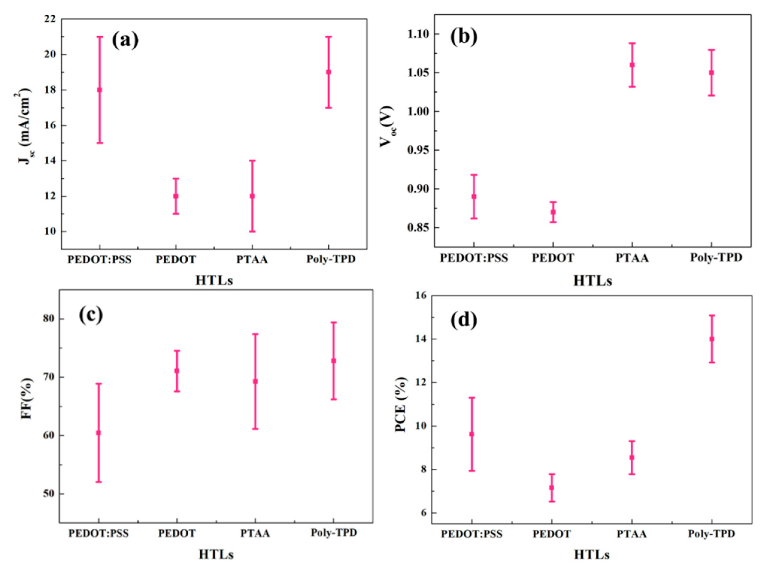
| HTL | FF (%) | Voc (V) | Jsc (mA/cm2) | PCE (%) |
|---|---|---|---|---|
| PEDOT: PSS | 60.4 ± 8.4 | 0.89 ± 0.03 | 18.0 ± 3.5 | 9.6 ± 1.7 |
| PEDOT | 71.1 ± 3.5 | 0.87 ± 0.01 | 11.6 ± 0.9 | 7.2 ± 0.6 |
| PTAA | 69.2 ± 8.1 | 1.06 ± 0.03 | 11.7 ± 2.0 | 8.5 ± 0.8 |
| Poly-TPD | 72.4 ± 6.7 | 1.05 ± 0.03 | 18.5 ± 2.3 | 14.0 ± 1.1 |
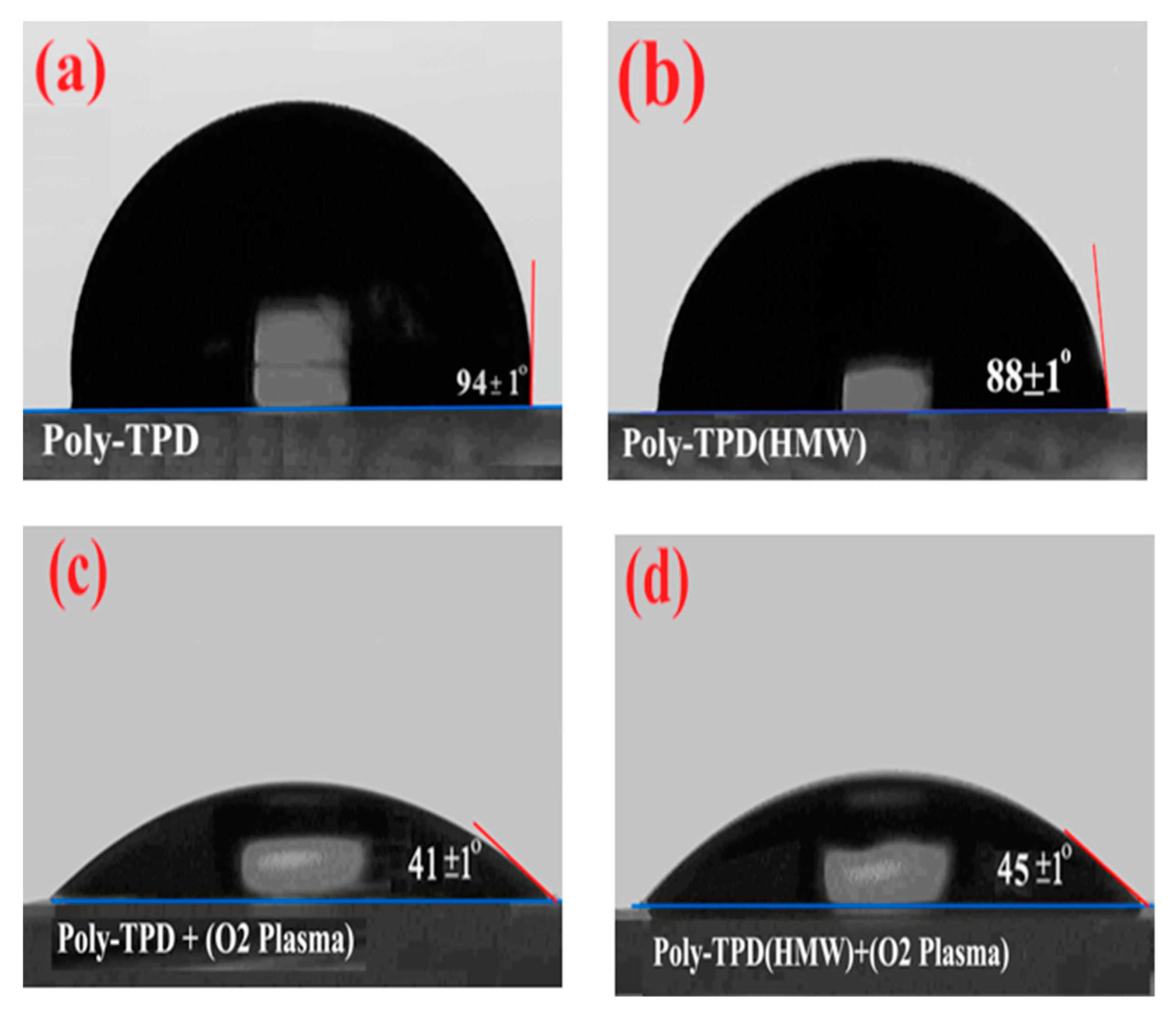
| Conditions | FF (%) | VOC (V) | JSC (mA/cm2) | PCE (%) |
|---|---|---|---|---|
| Treated Poly-TPD with UVO | 72.4 ± 6.7 | 1.05 ± 0.03 | 18.5 ± 2.3 | 14.0 ± 1.1 |
| Treated Poly-TPD (HMW) with UVO | 76.8 ± 2.4 | 1.05 ± 0.02 | 18.5 ± 1.0 | 15 ± 1.5 |
| Treated Poly-TPD with O2 Plasma | 43.3 ± 3 | 1.04 ± 0.03 | 14.3 ± 1.3 | 6.5 ± 1.0 |
| Treated Poly-TPD (HMW) with O2 Plasma | 47 ± 1 | 1.05 ± 0.01 | 15.6 ± 1.3 | 7.8 ± 0.9 |
© 2019 by the authors. Licensee MDPI, Basel, Switzerland. This article is an open access article distributed under the terms and conditions of the Creative Commons Attribution (CC BY) license (http://creativecommons.org/licenses/by/4.0/).
Share and Cite
Safari, Z.; Zarandi, M.B.; Giuri, A.; Bisconti, F.; Carallo, S.; Listorti, A.; Esposito Corcione, C.; Nateghi, M.R.; Rizzo, A.; Colella, S. Optimizing the Interface between Hole Transporting Material and Nanocomposite for Highly Efficient Perovskite Solar Cells. Nanomaterials 2019, 9, 1627. https://doi.org/10.3390/nano9111627
Safari Z, Zarandi MB, Giuri A, Bisconti F, Carallo S, Listorti A, Esposito Corcione C, Nateghi MR, Rizzo A, Colella S. Optimizing the Interface between Hole Transporting Material and Nanocomposite for Highly Efficient Perovskite Solar Cells. Nanomaterials. 2019; 9(11):1627. https://doi.org/10.3390/nano9111627
Chicago/Turabian StyleSafari, Zeinab, Mahmood Borhani Zarandi, Antonella Giuri, Francesco Bisconti, Sonia Carallo, Andrea Listorti, Carola Esposito Corcione, Mohamad Reza Nateghi, Aurora Rizzo, and Silvia Colella. 2019. "Optimizing the Interface between Hole Transporting Material and Nanocomposite for Highly Efficient Perovskite Solar Cells" Nanomaterials 9, no. 11: 1627. https://doi.org/10.3390/nano9111627
APA StyleSafari, Z., Zarandi, M. B., Giuri, A., Bisconti, F., Carallo, S., Listorti, A., Esposito Corcione, C., Nateghi, M. R., Rizzo, A., & Colella, S. (2019). Optimizing the Interface between Hole Transporting Material and Nanocomposite for Highly Efficient Perovskite Solar Cells. Nanomaterials, 9(11), 1627. https://doi.org/10.3390/nano9111627