Synthesis and Surface-Enhanced Raman Scattering of Ultrathin SnSe2 Nanoflakes by Chemical Vapor Deposition


Abstract
1. Introduction
2. Experimental Section
2.1. Synthesis of the SnSe2 Nanoflakes
2.2. Characterization of SnSe2 Nanoflakes
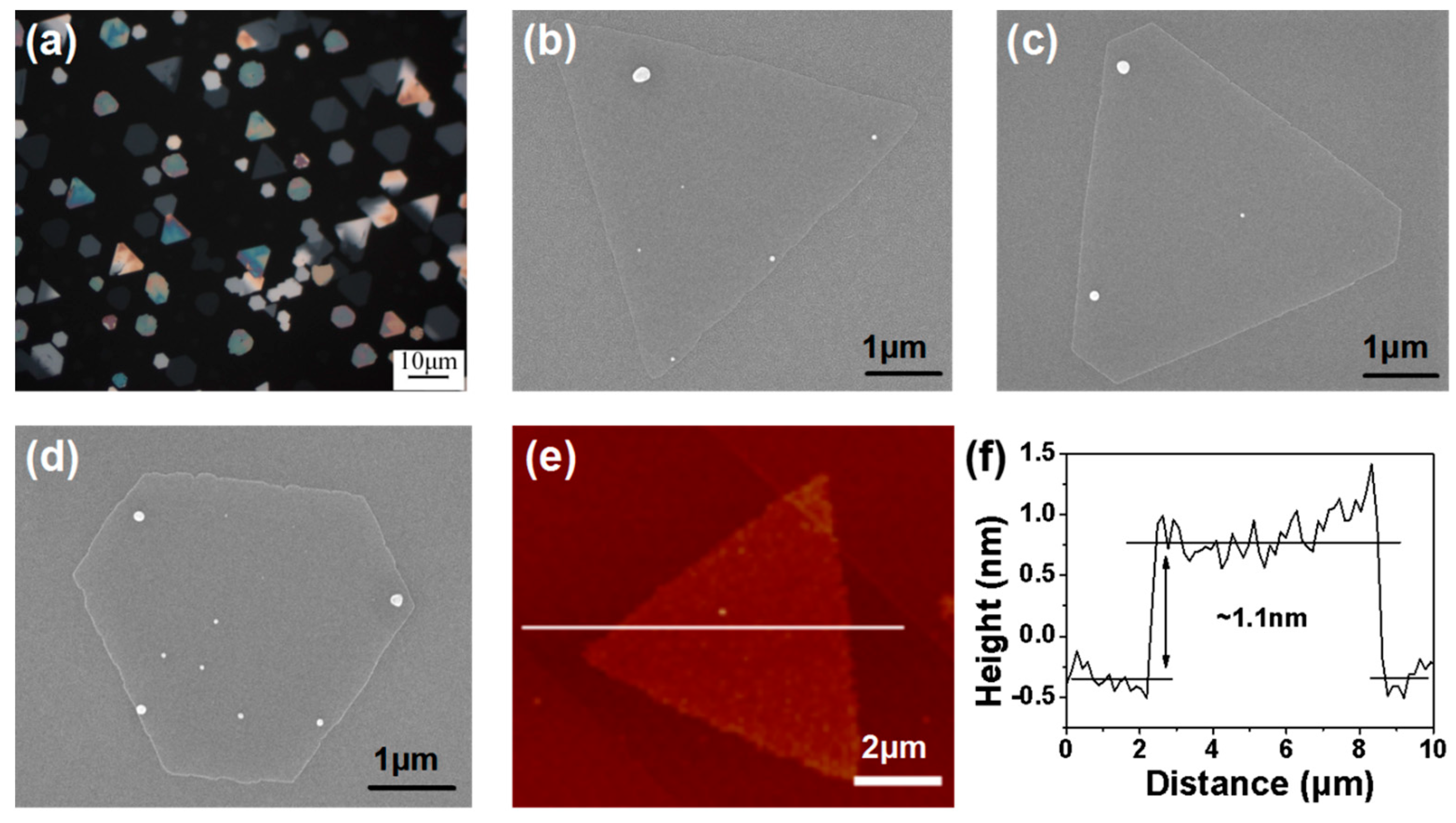
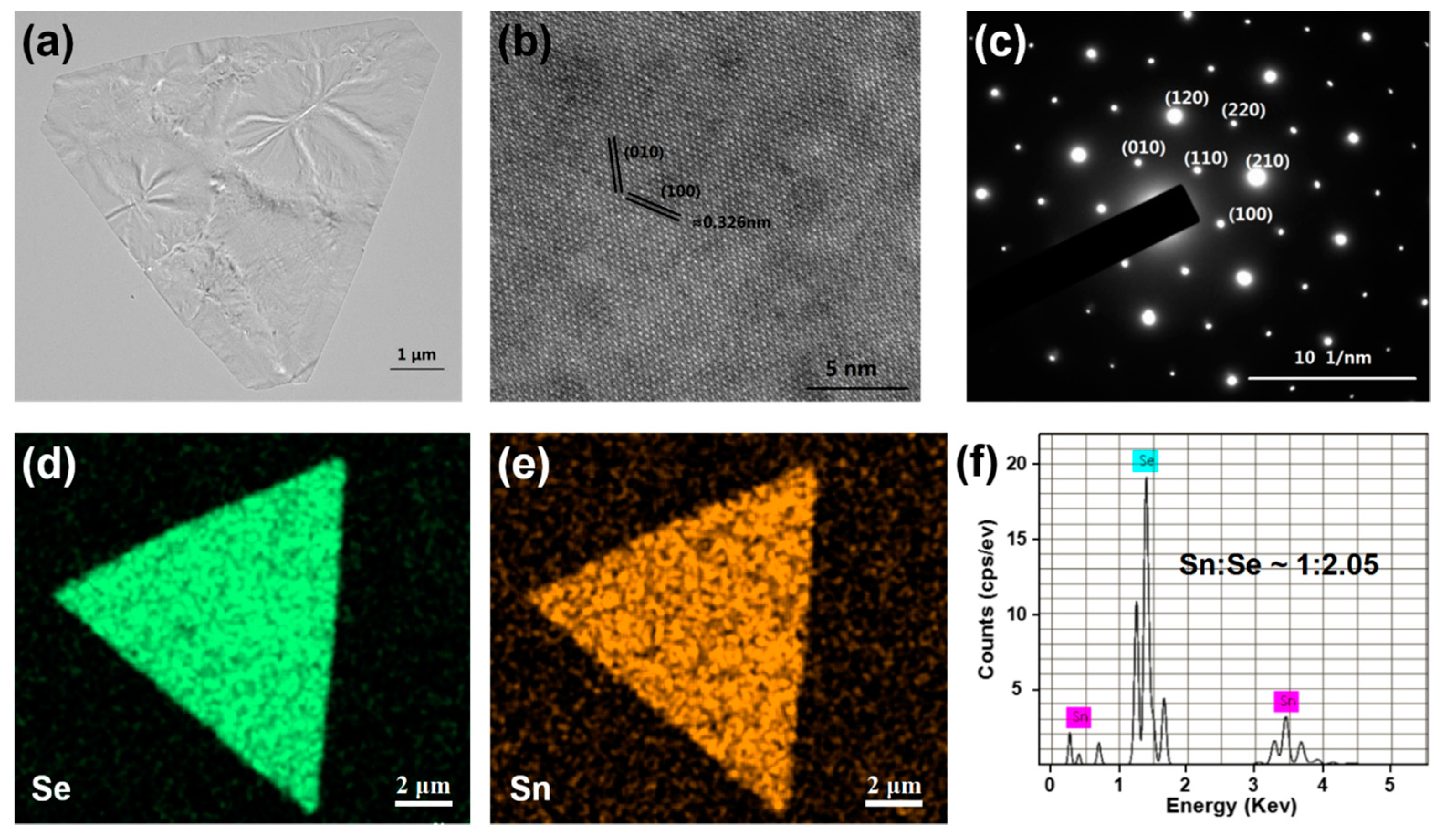
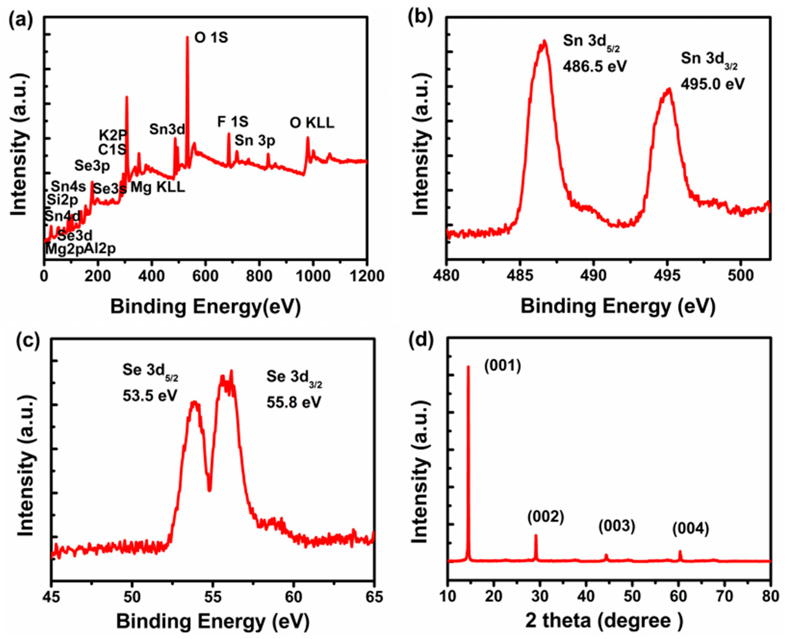
3. Results and Discussions
4. Conclusions
Supplementary Materials
Author Contributions
Funding
Conflicts of Interest
References
- Wang, Q.H.; Kalantar-Zadeh, K.; Kis, A.; Coleman, J.N.; Strano, M.S. Electronics and optoelectronics of two-dimensional transition metal dichalcogenides. Nat. Nanotechnol. 2012, 7, 699–712. [Google Scholar] [CrossRef] [PubMed]
- Mak, K.F.; Lee, C.; Hone, J.; Shan, J.; Heinz, T.F. Atomically thin MoS2: A new direct-gap semiconductor. Phys. Rev. Lett. 2010, 105, 136805. [Google Scholar] [CrossRef] [PubMed]
- Ji, Q.; Zhang, Y.; Zhang, Y.; Liu, Z. Chemical vapour deposition of group-VIB metal dichalcogenide monolayers: Engineered substrates from amorphous to single crystalline. Chem. Soc. Rev. 2015, 44, 2587–2602. [Google Scholar] [CrossRef] [PubMed]
- Novoselov, K.S.; Geim, A.K.; Morozov, S.V.; Jiang, D.; Zhang, Y.; Dubonos, S.V.; Grigorieva, I.V.; Firsov, A.A. Electric field effect in atomically thin carbon films. Science 2004, 306, 666–669. [Google Scholar] [CrossRef] [PubMed]
- Van der Zande, A.M.; Huang, P.Y.; Chenet, D.A.; Berkelbach, T.C.; You, Y.; Lee, G.H.; Heinz, T.F.; Reichman, D.R.; Muller, D.A.; Hone, J.C. Grains and grain boundaries in highly crystalline monolayer molybdenum disulphide. Nat. Mater. 2013, 12, 554–561. [Google Scholar] [CrossRef] [PubMed]
- Choi, W.; Cho, M.Y.; Konar, A.; Lee, J.H.; Cha, G.B.; Hong, S.C.; Kim, S.; Kim, J.; Jena, D.; Joo, J.; et al. High-detectivity multilayer MoS2 phototransistors with spectral response from ultraviolet to infrared. Adv. Mater. 2012, 24, 5832–5836. [Google Scholar] [CrossRef] [PubMed]
- Xia, J.; Huang, X.; Liu, L.Z.; Wang, M.; Wang, L.; Huang, B.; Zhu, D.D.; Li, J.J.; Gu, C.Z.; Meng, X.M. CVD synthesis of large-area, highly crystalline MoSe2 atomic layers on diverse substrates and application to photodetectors. Nanoscale 2014, 6, 8949–8955. [Google Scholar] [CrossRef] [PubMed]
- Baek, J.; Yin, D.; Liu, N.; Omkaram, I.; Jung, C.; Im, H.; Hong, S.; Kim, S.M.; Hong, Y.K.; Hur, J.; et al. Highly sensitive chemical gas detecting transistor based on highly crystalline CVD-grown MoSe2 films. Nano Res. 2016, 10, 1861–1871. [Google Scholar] [CrossRef]
- Gao, Y.; Hong, Y.-L.; Yin, L.-C.; Wu, Z.; Yang, Z.; Chen, M.-L.; Liu, Z.; Ma, T.; Sun, D.-M.; Ni, Z.; et al. Ultrafast growth of high-quality monolayer WSe2 on Au. Adv. Mater. 2017, 29, 1700990. [Google Scholar] [CrossRef] [PubMed]
- Huang, J.-K.; Pu, J.; Hsu, C.-L.; Chiu, M.-H.; Juang, Z.-Y.; Chang, Y.-H.; Chang, W.-H.; Iwasa, Y.; Takenobu, T.; Li, L.-J. Large-area synthesis of highly crystalline WSe2 monolayers and device applications. ACS Nano 2013, 8, 923–930. [Google Scholar] [CrossRef] [PubMed]
- Late, D.J.; Liu, B.; Luo, J.; Yan, A.; Matte, H.S.; Grayson, M.; Rao, C.N.; Dravid, V.P. GaS and GaSe ultrathin layer transistors. Adv. Mater. 2012, 24, 3549–3554. [Google Scholar] [CrossRef] [PubMed]
- Hu, P.; Wang, L.; Yoon, M.; Zhang, J.; Feng, W.; Wang, X.; Wen, Z.; Idrobo, J.C.; Miyamoto, Y.; Geohegan, D.B.; et al. Highly responsive ultrathin GaS nanosheet photodetectors on rigid and flexible substrates. Nano Lett. 2013, 13, 1649–1654. [Google Scholar] [CrossRef] [PubMed]
- Feng, W.; Zheng, W.; Cao, W.; Hu, P. Back gated multilayer InSe transistors with enhanced carrier mobilities via the suppression of carrier scattering from a dielectric interface. Adv. Mater. 2014, 26, 6587–6593. [Google Scholar] [CrossRef] [PubMed]
- Feng, W.; Wu, J.-B.; Li, X.; Zheng, W.; Zhou, X.; Xiao, K.; Cao, W.; Yang, B.; Idrobo, J.-C.; Basile, L.; et al. Ultrahigh photo-responsivity and detectivity in multilayer InSe nanosheets phototransistors with broadband response. J. Mater. Chem. C 2015, 3, 7022–7028. [Google Scholar] [CrossRef]
- Su, G.; Hadjiev, V.G.; Loya, P.E.; Zhang, J.; Lei, S.; Maharjan, S.; Dong, P.; P, M.A.; Lou, J.; Peng, H. Chemical vapor deposition of thin crystals of layered semiconductor SnS2 for fast photodetection application. Nano Lett. 2015, 15, 506–513. [Google Scholar] [CrossRef] [PubMed]
- Yang, D.; Li, B.; Hu, C.; Deng, H.; Dong, D.; Yang, X.; Qiao, K.; Yuan, S.; Song, H. Controllable growth orientation of SnS2 flakes for low-noise, high-photoswitching ratio, and ultrafast phototransistors. Adv. Opt. Mater. 2016, 4, 419–426. [Google Scholar] [CrossRef]
- Acerce, M.; Voiry, D.; Chhowalla, M. Metallic 1T phase MoS2 nanosheets as supercapacitor electrode materials. Nat. Nanotechnol. 2015, 10, 313–318. [Google Scholar] [CrossRef] [PubMed]
- Huang, X.; Zeng, Z.; Zhang, H. Metal dichalcogenide nanosheets: Preparation, properties and applications. Chem. Soc. Rev. 2013, 42, 1934–1946. [Google Scholar] [CrossRef] [PubMed]
- Fiori, G.; Bonaccorso, F.; Iannaccone, G.; Palacios, T.; Neumaier, D.; Seabaugh, A.; Banerjee, S.K.; Colombo, L. Electronics based on two-dimensional materials. Nat. Nanotechnol. 2014, 9, 768–779. [Google Scholar] [CrossRef] [PubMed]
- Yu, P.; Yu, X.; Lu, W.; Lin, H.; Sun, L.; Du, K.; Liu, F.; Fu, W.; Zeng, Q.; Shen, Z.; et al. Fast photoresponse from 1T tin diselenide atomic layers. Adv. Funct. Mater. 2016, 26, 137–145. [Google Scholar] [CrossRef]
- Zhou, X.; Gan, L.; Tian, W.; Zhang, Q.; Jin, S.; Li, H.; Bando, Y.; Golberg, D.; Zhai, T. Ultrathin SnSe2 flakes grown by chemical vapor deposition for high-performance photodetectors. Adv. Mater. 2015, 27, 8035–8041. [Google Scholar] [CrossRef] [PubMed]
- Choi, J.; Jin, J.; Jung, I.G.; Kim, J.M.; Kim, H.J.; Son, S.U. SnSe2 nanoplate-graphene composites as anode materials for lithium ion batteries. Chem. Commun. 2011, 47, 5241–5243. [Google Scholar] [CrossRef] [PubMed]
- Yu, X.; Zhu, J.; Zhang, Y.; Weng, J.; Hu, L.; Dai, S. SnSe2 quantum dot sensitized solar cells prepared employing molecular metal chalcogenide as precursors. Chem. Commun. 2012, 48, 3324–3326. [Google Scholar] [CrossRef] [PubMed]
- Zhang, C.; Yin, H.; Han, M.; Dai, Z.; Pang, H.; Zheng, Y.; Lan, Y.-Q.; Bao, J.; Zhu, J. Two-dimensional tin selenide nanostructures for flexible all-solid-state supercapacitors. ACS Nano 2014, 8, 3761–3770. [Google Scholar] [CrossRef] [PubMed]
- Huang, Y.; Xu, K.; Wang, Z.; Shifa, T.A.; Wang, Q.; Wang, F.; Jiang, C.; He, J. Designing the shape evolution of SnSe2 nanosheets and their optoelectronic properties. Nanoscale 2015, 7, 17375–17380. [Google Scholar] [CrossRef] [PubMed]
- Wang, R.Y.; Caldwell, M.A.; Jeyasingh, R.G.D.; Aloni, S.; Shelby, R.M.; Wong, H.S.P.; Milliron, D.J. Electronic and optical switching of solution-phase deposited SnSe2 phase change memory material. J. Appl. Phys. 2011, 109, 113506. [Google Scholar] [CrossRef]
- Zhou, W.; Yu, Z.; Song, H.; Fang, R.; Wu, Z.; Li, L.; Ni, Z.; Ren, W.; Wang, L.; Ruan, S. Lattice dynamics in monolayer and few-layer SnSe2. Phys. Rev. B 2017, 96. [Google Scholar] [CrossRef]
- Liu, K.; Liu, H.; Wang, J.; Feng, L. Synthesis and characterization of SnSe2 hexagonal nanoflakes. Mater. Lett. 2009, 63, 512–514. [Google Scholar] [CrossRef]
- Fang, Z.; Hao, S.; Long, L.; Fang, H.; Qiang, T.; Song, Y. The enhanced photoelectrochemical response of SnSe2 nanosheets. CrystEngComm 2014, 16, 2404–2410. [Google Scholar] [CrossRef]
- Park, Y.W.; Jerng, S.-K.; Jeon, J.H.; Roy, S.B.; Akbar, K.; Kim, J.; Sim, Y.; Seong, M.-J.; Kim, J.H.; Lee, Z.; et al. Molecular beam epitaxy of large-area SnSe2 with monolayer thickness fluctuation. 2D Mater. 2016, 4, 014006. [Google Scholar] [CrossRef]
- Wu, J.; Hu, Z.; Jin, Z.; Lei, S.; Guo, H.; Chatterjee, K.; Zhang, J.; Yang, Y.; Li, B.; Liu, Y.; et al. Spiral growth of SnSe2 crystals by chemical vapor deposition. Adv. Mater. Interfaces 2016, 3, 1600383. [Google Scholar] [CrossRef]
- Huang, L.; Yu, Y.; Li, C.; Cao, L. Substrate mediation in vapor deposition growth of layered chalcogenide nanoplates: A case study of SnSe2. J. Phys. Chem. C 2013, 117, 6469–6475. [Google Scholar] [CrossRef]
- Gong, Y.; Lei, S.; Ye, G.; Li, B.; He, Y.; Keyshar, K.; Zhang, X.; Wang, Q.; Lou, J.; Liu, Z.; et al. Two-step growth of two-dimensional WSe2/MoSe2 heterostructures. Nano Lett. 2015, 15, 6135–6141. [Google Scholar] [CrossRef] [PubMed]
- Peng, H.; Dang, W.; Cao, J.; Chen, Y.; Wu, D.; Zheng, W.; Li, H.; Shen, Z.X.; Liu, Z. Topological insulator nanostructures for near-infrared transparent flexible electrodes. Nat. Chem. 2012, 4, 281–286. [Google Scholar] [CrossRef] [PubMed]
- Hu, Y.; Chen, T.; Wang, X.; Ma, L.; Chen, R.; Zhu, H.; Yuan, X.; Yan, C.; Zhu, G.; Lv, H.; et al. Controlled growth and photoconductive properties of hexagonal SnS2 nanoflakes with mesa-shaped atomic steps. Nano Res. 2017, 10, 1434–1447. [Google Scholar] [CrossRef]
- Ma, D.; Shi, J.; Ji, Q.; Chen, K.; Yin, J.; Lin, Y.; Zhang, Y.; Liu, M.; Feng, Q.; Song, X.; et al. A universal etching-free transfer of MoS2 films for applications in photodetectors. Nano Res. 2015, 8, 3662–3672. [Google Scholar] [CrossRef]
- Sahabudeen, H.; Qi, H.; Glatz, B.A.; Tranca, D.; Dong, R.; Hou, Y.; Zhang, T.; Kuttner, C.; Lehnert, T.; Seifert, G.; et al. Wafer-sized multifunctional polyimine-based two-dimensional conjugated polymers with high mechanical stiffness. Nat. Commun. 2016, 7, 13461. [Google Scholar] [CrossRef] [PubMed]
- Lee, Y.H.; Zhang, X.Q.; Zhang, W.; Chang, M.T.; Lin, C.T.; Chang, K.D.; Yu, Y.C.; Wang, J.T.; Chang, C.S.; Li, L.J.; et al. Synthesis of large-area MoS2 atomic layers with chemical vapor deposition. Adv. Mater. 2012, 24, 2320–2325. [Google Scholar] [CrossRef] [PubMed]
- Zhan, Y.; Liu, Z.; Najmaei, S.; Ajayan, P.M.; Lou, J. Large-area vapor-phase growth and characterization of MoS2 atomic layers on a SiO2 substrate. Small 2012, 8, 966–971. [Google Scholar] [CrossRef] [PubMed]
- De Groot, C.H.; Gurnani, C.; Hector, A.L.; Huang, R.; Jura, M.; Levason, W.; Reid, G. Highly selective chemical vapor deposition of tin diselenide thin films onto patterned substrates via single source diselenoether precursors. Chem. Mater. 2012, 24, 4442–4449. [Google Scholar] [CrossRef]
- Saha, S.; Banik, A.; Biswas, K. Few-layer nanosheets of n-type SnSe2. Chem.-Eur. J. 2016, 22, 15634–15638. [Google Scholar] [CrossRef] [PubMed]
- Velicky, M.; Toth, P.S.; Rakowski, A.M.; Rooney, A.P.; Kozikov, A.; Woods, C.R.; Mishchenko, A.; Fumagalli, L.; Yin, J.; Zolyomi, V.; et al. Exfoliation of natural van der waals heterostructures to a single unit cell thickness. Nat. Commun. 2017, 8, 14410. [Google Scholar] [CrossRef] [PubMed]
- Harbec, J.Y.; Powell, B.M.; Jandl, S. Lattice dynamics of SnSe2. Phys. Rev. B 1983, 28, 7009–7013. [Google Scholar] [CrossRef]
- Smith, A.; Meek, P.; Liang, W. Raman scattering studies of SnS2 and SnSe2. J. Phys. C Solid State Phys. 1977, 10, 1321. [Google Scholar] [CrossRef]
- Hu, P.; Wen, Z.; Wang, L.; Tan, P.; Xiao, K. Synthesis of few-layer GaSe nanosheets for high performance photodetectors. ACS Nano 2012, 6, 5988–5994. [Google Scholar] [CrossRef] [PubMed]
- Lorchat, E.; Froehlicher, G.; Berciaud, S. Splitting of interlayer shear modes and photon energy dependent anisotropic Raman response in n-layer ReSe2 and ReS2. ACS Nano 2016, 10, 2752–2760. [Google Scholar] [CrossRef] [PubMed]
- Michaels, A.M.; Jiang, J.; Brus, L. Ag nanocrystal junctions as the site for surface-enhanced Raman scattering of single rhodamine 6G molecules. J. Phys. Chem. B 2000, 104, 11965–11971. [Google Scholar] [CrossRef]
- Lee, Y.; Kim, H.; Lee, J.; Yu, S.H.; Hwang, E.; Lee, C.; Ahn, J.-H.; Cho, J.H. Enhanced Raman scattering of rhodamine 6G films on two-dimensional transition metal dichalcogenides correlated to photoinduced charge transfer. Chem. Mater. 2015, 28, 180–187. [Google Scholar] [CrossRef]
- Campion, A.; Kambhampati, P. Surface-enhanced Raman scattering. Chem. Soc. Rev. 1998, 27, 241. [Google Scholar] [CrossRef]
- Ling, X.; Xie, L.; Fang, Y.; Xu, H.; Zhang, H.; Kong, J.; Dresselhaus, M.S.; Zhang, J.; Liu, Z. Can graphene be used as a substrate for Raman enhancement? Nano Lett. 2010, 10, 553–561. [Google Scholar] [CrossRef] [PubMed]


© 2018 by the authors. Licensee MDPI, Basel, Switzerland. This article is an open access article distributed under the terms and conditions of the Creative Commons Attribution (CC BY) license (http://creativecommons.org/licenses/by/4.0/).
Share and Cite
Zhang, Y.; Shi, Y.; Wu, M.; Zhang, K.; Man, B.; Liu, M. Synthesis and Surface-Enhanced Raman Scattering of Ultrathin SnSe2 Nanoflakes by Chemical Vapor Deposition. Nanomaterials 2018, 8, 515. https://doi.org/10.3390/nano8070515
Zhang Y, Shi Y, Wu M, Zhang K, Man B, Liu M. Synthesis and Surface-Enhanced Raman Scattering of Ultrathin SnSe2 Nanoflakes by Chemical Vapor Deposition. Nanomaterials. 2018; 8(7):515. https://doi.org/10.3390/nano8070515
Chicago/Turabian StyleZhang, Yongheng, Ying Shi, Meimei Wu, Kun Zhang, Baoyuan Man, and Mei Liu. 2018. "Synthesis and Surface-Enhanced Raman Scattering of Ultrathin SnSe2 Nanoflakes by Chemical Vapor Deposition" Nanomaterials 8, no. 7: 515. https://doi.org/10.3390/nano8070515
APA StyleZhang, Y., Shi, Y., Wu, M., Zhang, K., Man, B., & Liu, M. (2018). Synthesis and Surface-Enhanced Raman Scattering of Ultrathin SnSe2 Nanoflakes by Chemical Vapor Deposition. Nanomaterials, 8(7), 515. https://doi.org/10.3390/nano8070515