Article

High-Switching-Ratio Photodetectors Based on Perovskite CH3NH3PbI3 Nanowires

1
School of Materials Science and Engineering, Hebei University of Technology, Tianjin 300132, China
2
School of Xingtai Polytechnic College, Xingtai 054035, China
*
Authors to whom correspondence should be addressed.
Nanomaterials 2018, 8(5), 318; https://doi.org/10.3390/nano8050318
Submission received: 16 April 2018 / Revised: 1 May 2018 / Accepted: 2 May 2018 / Published: 10 May 2018

Abstract

:
Hybrid organic-inorganic perovskite materials have attracted extensive attention due to their impressive performance in photovoltaic devices. One-dimensional perovskite CH3NH3PbI3 nanomaterials, possessing unique structural features such as large surface-to-volume ratio, anisotropic geometry and quantum confinement, may have excellent optoelectronic properties, which could be utilized to fabricate high-performance photodetectors. However, in comparison to CH3NH3PbI3 thin films, reports on the fabrication of CH3NH3PbI3 nanowires for optoelectrical application are rather limited. Herein, a two-step spin-coating process has been utilized to fabricate pure-phase and single-crystalline CH3NH3PbI3 nanowires on a substrate without mesoporous TiO2 or Al2O3. The size and density of CH3NH3PbI3 nanowires can be easily controlled by changing the PbI2 precursor concentration. The as-prepared CH3NH3PbI3 nanowires are utilized to fabricate photodetectors, which exhibit a fairly high switching ratio of ~600, a responsivity of 55 mA/W, and a normalized detectivity of 0.5 × 10¹¹ jones under 532 nm light illumination (40 mW/cm2) at a very low bias voltage of 0.1 V. The as-prepared perovskite CH3NH3PbI3 nanowires with excellent optoelectronic properties are regarded to be a potential candidate for high-performance photodetector application.

Graphical Abstract

1. Introduction

Photodetectors, which convert incident light signals into electronic signals, are important devices for application in a wide range of civilian and military fields, including optical communications, environmental sensors, medical analysis, missile launch detection, and so forth [1,2,3]. The crucial characteristics of high-performance photodetectors for practical application include wide spectral response, sensitivity, high switching ratio, fast response, large detectivity and easy fabrication. Many semiconductor nanomaterials, such as ZnO, Si, CdS, PbS, CdHgTe, have been applied in photodetectors that can detect the light ranged from UV to infrared region [4,5,6]. Recently, hybrid organic-inorganic perovskite materials, such as CH3NH3PbI3 (MAPbI3), have been extensively studied and applied in solar cells [7,8,9], LEDs [10,11] and laser devices [12] due to their distinct photoelectric properties, which include high absorption coefficient, direct and tunable bandgap, weak exciton binding energy, high carrier mobility and long carrier-diffusion lengths.
In the past few decades, one-dimensional (1D) semiconductor nanomaterials have been considered the most promising candidates for achieving high-performance photodetectors with high switching ratio (SR), large responsivity (Rλ), fast response speed and excellent stability, which can be attributed to their large surface-to-volume ratio, anisotropic geometry and quantum confinement in two dimensions [13]. Therefore, the fabrication of 1D perovskite MAPbI3 nanomaterials has attracted significant interest from researchers. Several methods have been successfully utilized to prepare MAPbI3 nanowires or microwires, including slip-coating method [14], dissolution-recrystallization process [15], template guide growth technology [16,17], inkjet printing method [18], and so on. However, in comparison to MAPbI3 thin films [19,20,21], the reports about the fabrication of MAPbI3 nanowires for application in optoelectrical application [22,23] are rather limited. In addition, some reports also indicate that single-crystalline perovskite nanowires have very low defect levels and impressive optoelectrical properties [24,25,26], which are comparable or even better than their large single-crystal counterpart. Therefore, developing a high-efficiency photodetector based on single-crystalline perovskite nanowires is of great significance.
Recently, a two-step spin-coating process, which was firstly reported by Park’s group, was utilized to synthesize CH3NH3PbI3 nanowires on a mesoporous TiO2 or Al2O3 substrate for application in perovskite solar cell, with a power conversion efficiency (PCE) of 14.71% at standard AM (Path-length through the atmosphere relative to vertical thickness of the atmosphere) 1.5 G solar illumination [27]. However, as far as we know, scarcely any works have been reported that use the two-step spin-coating process to prepare single MAPbI3 nanowires on a substrate without mesoporous TiO2 or Al2O3 and apply them in photodetectors. In this work, we improved the two-step spin-coating process to fabricate pure-phase and single-crystalline MAPbI3 nanowires with various densities and sizes on a SiO2/Si substrate just by changing the PbI2 precursor concentration. The as-prepared MAPbI3 nanowires were used to fabricate photodetectors that exhibited a fairly high switching ratio of ~600, responsivity of 55 mA/W and normalized detectivity of 0.5 × 10¹¹ jones under 532 nm light illumination (40 mW/cm2) at a very low bias voltage of 0.1 V. To the best of our knowledge, the high switching ratio is one of the best results among previously reported perovskite-based photodetectors [15,19,20,21,22,23,28]. The MAPbI3 nanowires with excellent optoelectronic properties may be an ideal choice for high-performance photodetectors.

2. Materials and Methods

2.1. Materials and Chemicals

Lead iodide (PbI2, 99.9%, Aladdin, Shanghai, China), N,N-dimethylformamide (DMF, 99%, Aladdin), methylamine (CH3NH2, 33% in absolute methanol, Aladdin), hydroiodic acid (HI, 58 wt % in water, Aladdin), Lead iodide (C2H5OH, 99.9%, Aladdin), Isopropanol (C3H8O, 99.9%, Aladdin), Ethyl ether (C4H10O, 99.9%, Aladdin). All chemicals were used as received.

2.2. Preparation of CH3NH3I (MAI)

CH3NH3I was prepared according to the reported process with some modifications [17]. Typically, 24 mL methylamine (CH3NH2) (33 wt % in absolute methanol, Aladdin, China) and 10 mL of hydroiodic acid (HI) (58 wt % in water, Aladdin, Shanghai, China) were in a 250 mL round-bottom flask at 0 °C for 2 h with stirring to synthesize. The precipitate was collected by evaporating the solvents on a rotary evaporator at 50 °C. The MAI product was washed and precipitated with the addition of the absolute ethanol and diethyl ether for three times, respectively. The solid was collected and dried at 60 °C in a vacuum oven for 24 h.

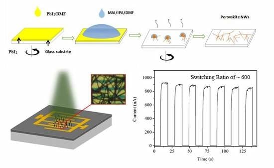
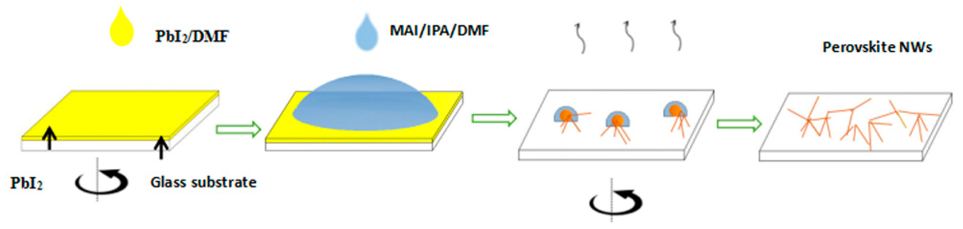
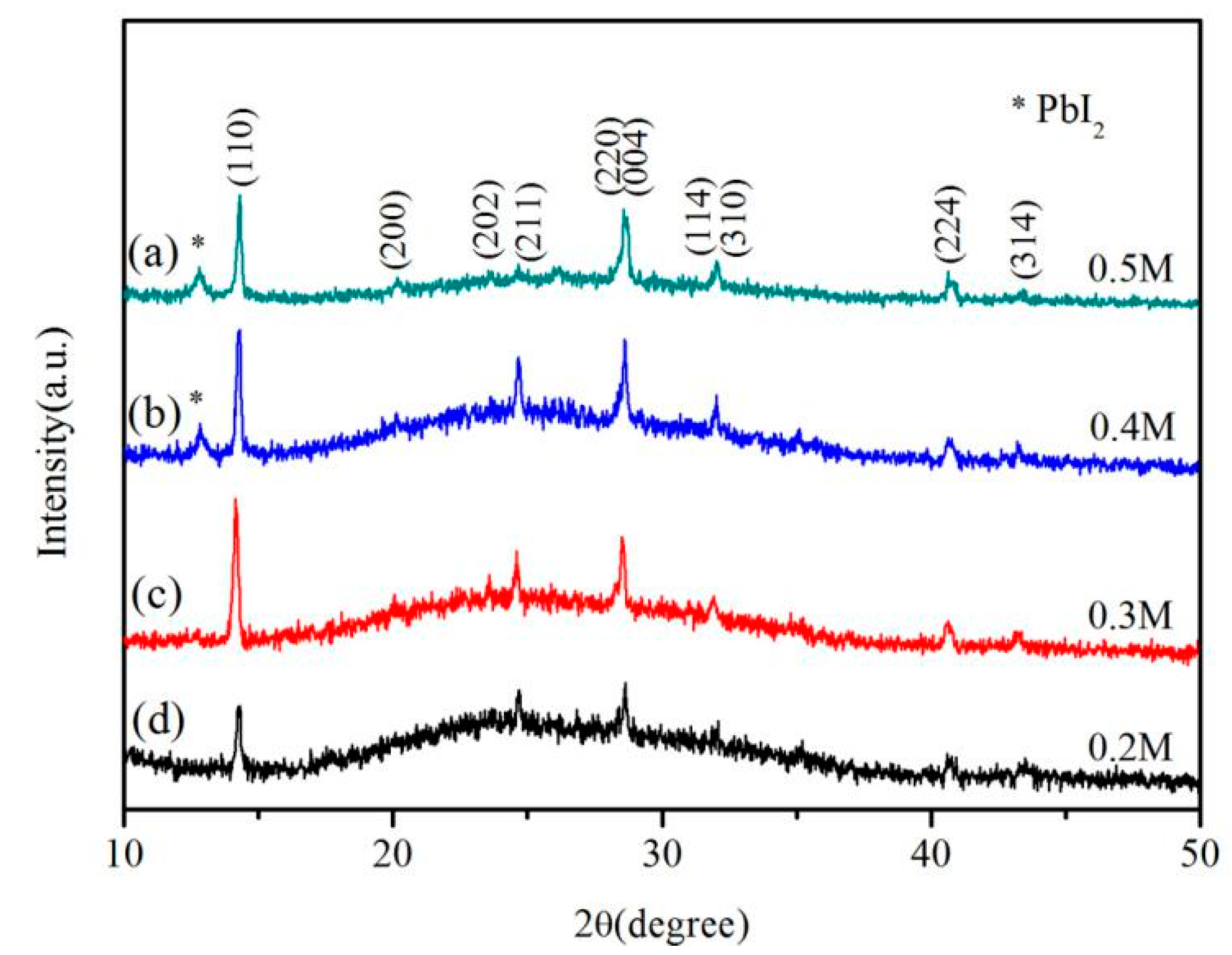
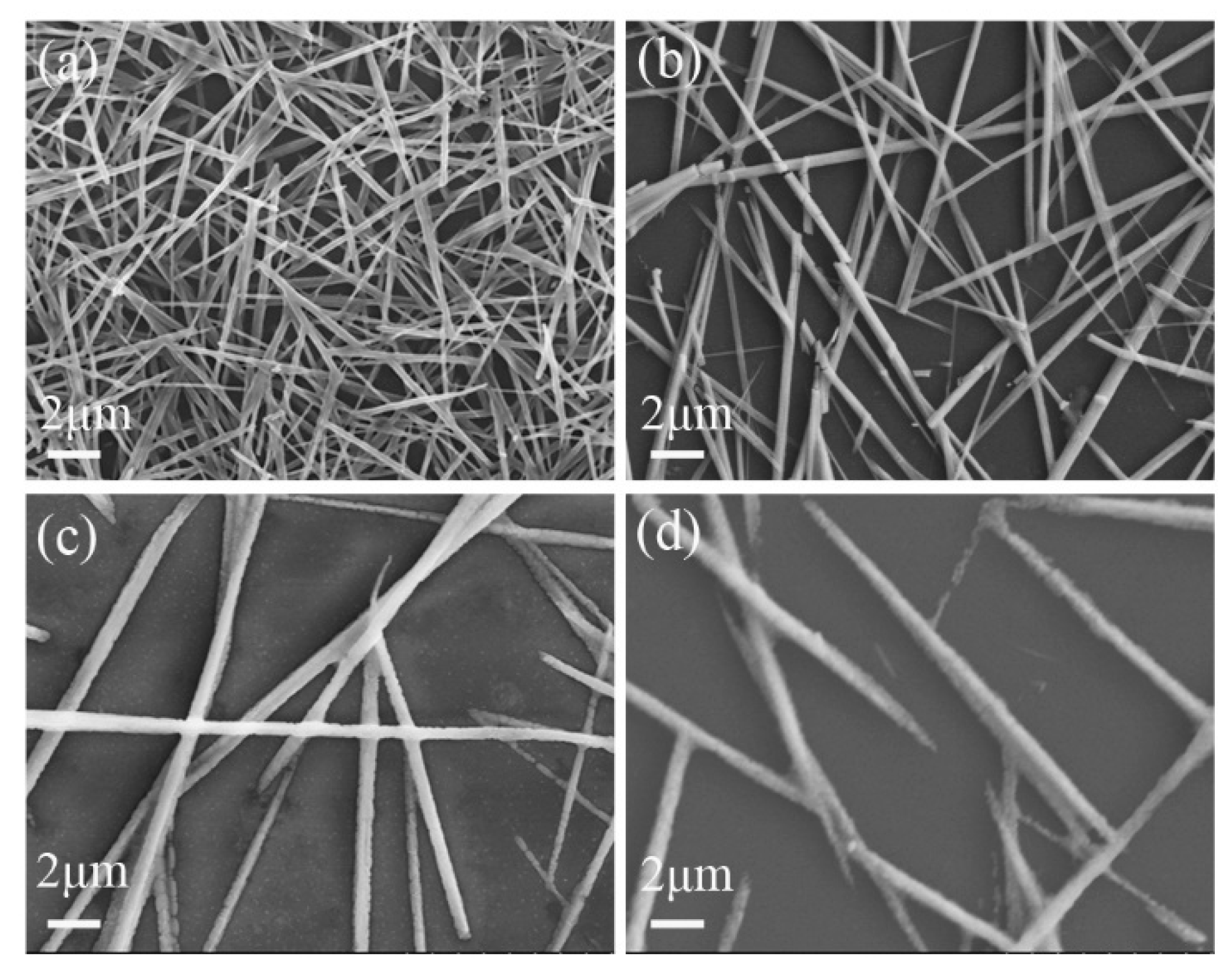
2.3. Preparation of CH3NH3PbI3 (MAPbI3) Nanowires

The SiO2/Si substrates were cleaned in an ultrasonic bath with acetone, isopropyl and ethanol for 5 min, respectively, and dried with clean N2 for further use. MAPbI3 nanowires were formed using the two-step spin-coating process. Firstly, to deposit PbI2 precursor layer, PbI2 precursor solution with different concentrations of 0.5 M, 0.4 M, 0.3 M and 0.2 M, respectively, was prepared by dissolving a certain amount of PbI2 in 2 mL of DMF and stirring in room temperature. Then, 20 μL of PbI2 precursor solution was loaded on the substrate for 10 s, followed by spinning at 2000 rpm for 5 s and 6000 rpm for 5 s. Secondly, 17.5 mg MAI powders were poured in 5 mL isopropanol (IPA), including 5 μL of DMF, and then stirred at room temperature until dissolved. 200 μL of the MAI-IPA solution was loaded on the PbI2-coated substrate for 40 s, followed by spinning at 4000 rpm for 20 s and drying at 100 °C in an oven for 5 min. Finally, the final MAPbI3 nanowires with different size and density can be obtained. All of the process were in air.

2.4. Device Fabrication

The interdigital Au electrodes with interfinger distance of 4 μm and length of 1000 μm were fabricated on SiO2/Si substrates using the conventional lithography technique. The abovementioned MAPbI3 nanowires synthesized with different concentrations of PbI2 precursor solution were spin-coated on the interdigitated Au electrodes for further photoelectric characterization.

2.5. Structural Characterization
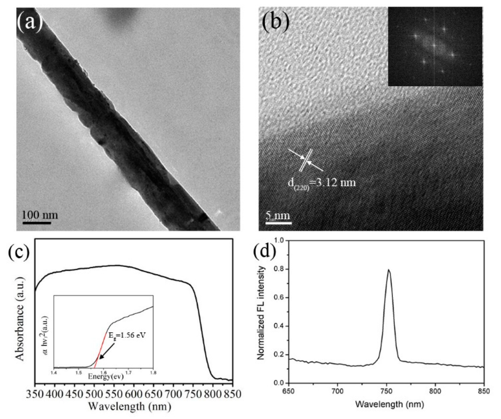
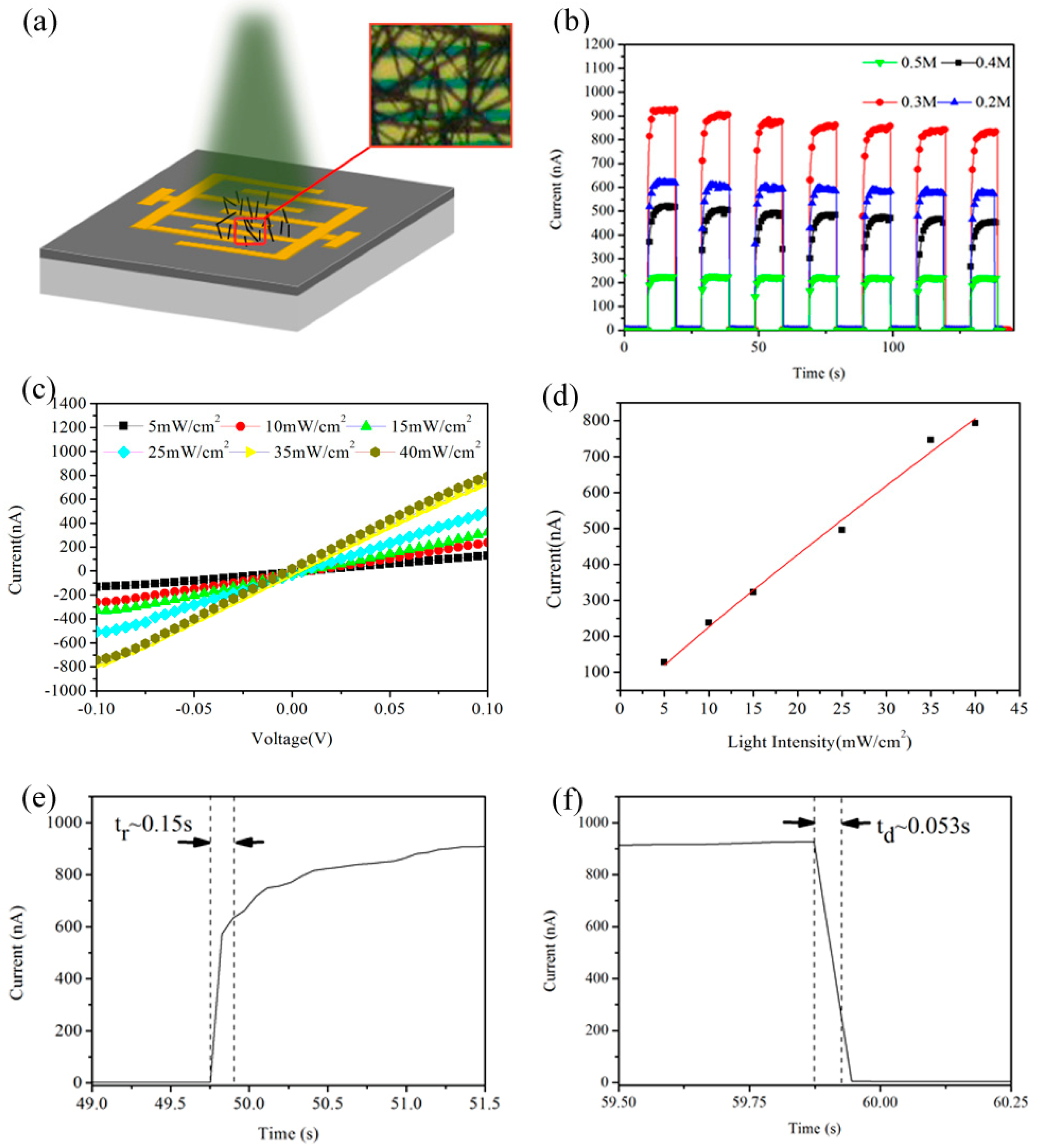
X-ray diffraction (XRD) was detected by Rigaku D/Max 2500 V/PC X-ray powder diffractometer (Hitachi, Tokyo, Japan) with CuKa radiation. FESEM (Rigaku, Tokyo, Japan) morphology and Energy Dispersive X-ray Fluorescence (EDX) analyses were performed using a Hatchi s-4800 field emission scanning electron microscope (Hitachi, Tokyo, Japan). Transmission electron microscopy (TEM) and high-resolution transmission electron microscopy (HRTEM) were performed using a Tecnai G2 F20 field emission transmission electron microscope (FETEM) (Philippe, Amsterdam, The Netherlands). Absorption spectra were recorded by a U-3900 H Spectrophotometer with optics integrating sphere (Hitachi, Tokyo, Japan). Fluorescence spectra were recorded with an F-7000 FL spectrofluorometer (Japan High-tech Corporation, Tokyo, Japan). Photoresponse characterization were done using a digital sourcemeter (keithley 2400) and a monochromatic light source (Bo Feilai Technology Co., Ltd., Beijing, China).

3. Results

Figure 1 presents the two-step spin-coating process scheme for synthesizing perovskite nanowires. Firstly, PbI2-DMF precursor solution with different concentrations was spin coated onto a SiO2/Si substrate to form PbI2 thin films, which was called the first spin-coating stage. Secondly, 200 μL MAI-IPA solution (17.5 mg MAI/5 mL IPA), including 5 μL DMF solution, was loaded on the PbI2 thin films for 10 s followed by spin coating, which was called the second spin-coating stage. Then, the obtained films were annealed in an oven. Finally, the perovskite MAPbI3 nanowires were obtained.
Figure 2 shows the XRD patterns of the perovskite nanowires synthesized with different PbI2 concentration of 0.5 M, 0.4 M, 0.3 M and 0.2 M. The main diffraction peaks at 2θ = 14.20°, 24.49°, 28.32°, 28.49°, 31.82° and 40.79° (Figure 2a,b) correspond to (110), (211), (004), (220), (310) and (224) planes of the tetragonal perovskite MAPbI3, which are in agreement with the references [15,27,29,30]. In addition, the weak diffraction peak at 2θ = 12.7° shown in Figure 2a,b can be indexed to the (001) plane of hexagonal PbI2 (JCPDS. No. 07-0235), indicating that a small amount of PbI2 was present in the products. Further decreasing the PbI2 concentration to 0.3 M and 0.2 M (Figure 2c,d), the products are composed of pure-phase tetragonal perovskite MAPbI3. Furthermore, the PbI2 concentration will also affect the size and density of the synthesized MAPbI3 nanowires, which is shown in Figure 3. It can be clearly seen that, with the decrease of PbI2 concentration from 0.5 M to 0.2 M, the size of MAPbI3 nanowires will increase, with the average diameter increasing from 180 nm to 850 nm and the average length increasing from several microns to dozens of microns, while the density of MAPbI3 nanowires decreases. In addition, the size distribution of the MAPbI3 nanowires become more broaden with the decrease of PbI2 concentration in the first spin-coating step.
As is well known, DMF is a benign solvent, while IPA is a poor solvent for PbI2. A small amount of DMF in IPA solution will dissolve PbI2 after dropping it on PbI2 precursor films, which will form a liquid cluster containing dissolved PbI2 and MAI molecules [27]. During the secondary spin-coating stage, the rapid evaporation of solvent will lead to sudden supersaturation and form quick nucleation of perovskite MAPbI3. Furthermore, the tetragonal perovskite MAPbI3 has a tendency to form nanowires by self-assembly of particles [15], which is also confirmed in Figure S1. Along with decreasing the PbI2 concentration during the first spin-coating process, the supersaturation level of perovskite MAPbI3 in solution will also decrease, leading to fewer nucleation centers and lower density of nanowires. Due to the smaller number of nuclei, fewer monomers are exhausted at the stage of nucleation, which can be utilized to encourage each nucleus to increase in size at the stage of crystal growth, leading to a larger size of MAPbI3 nanowires. This is consistent with the SEM (Transmission electron microscopy images) images in Figure 3. Therefore, the supersaturation level of perovskite MAPbI3 in solution is a crucial factor in influencing the final morphologies of perovskite nanowires. In addition to PbI2 concentration in the first spin-coating stage, the DMF concentration and MAI concentration in IPA in the secondary spin-coating stage can also effectively influence the kinetics of nanowire growth. It’s easy to conclude that, with the decrease of DMF concentration and the increase of MAI concentration in IPA, the supersaturation level of monomer solution will increase and generate more nucleation centers, leading to higher density of perovskite MAPbI3 nanowires with smaller size, which is consistent with the SEM results in Figures S2 and S3. TEM and HRTEM images of one typical perovskite MAPbI3 nanowire are presented in Figure 4a,b. It can be seen that the perovskite nanowire has a uniform diameter, which is shown in Figure 4a. The clear crystalline lattice and identical orientation to the typical nanowire indicate that it’s a single crystal with an interplanar distance of 0.312 nm, which corresponds to the (220) plane of tetragonal perovskite MAPbI3 (Figure 4b). The FFT image inserted in Figure 4b also demonstrates that the perovskite nanowire is a single crystal. Figure 4c shows the UV-Vis absorption spectra of the perovskite MAPbI3 nanowires. This result indicates that the MAPbI3 nanowires exhibit a strong and broad range of light absorption from 350 to 800 nm, which absolutely covers the entire visible light spectrum. The band gap calculated by Tauc’s formula shown in the insert of Figure 4c is about 1.56 eV, which agrees well with the reported perovskite MAPbI3 nanowires [27]. In addition, the MAPbI3 nanowires display a strong and sharp photoluminescence peak situated at 755 nm, which is almost consistent with the reported literature [27].
In order to further study the photoresponse properties of the MAPbI3 nanowires, a photodetector based on MAPbI3 nanowires was fabricated, with a schematic illustration shown in Figure 5a. The interdigital Au electrodes with an interfinger distance of 4 μm and a length of 1000 μm were prepared on SiO2/Si substrates using the conventional lithography technique. The pure-phase MAPbI3 nanowires synthesized with 0.3 M PbI2 precursor solution were spin-coated on the interdigitated electrodes. The key parameters of photodetectors are the switching ratio (SR), responsivity (R), detectivity (D*) and response speed [31]. The switching ratio is defined as SR = ((IpId)/Id), where Ip is photocurrent, Id is dark current. Responsivity can be calculated by R = ((IpId)/(P·S). P is the light power intensity and S is the effective sensitive areas, which are defined as the coverage areas of the interdigital Au electrodes by the MAPbI3 nanowires. Considering that the shot noise dominates the total noise in photoconductive photodetectors, normalized detectivity can be given by D* = ((IpId)/(P(2 e·Id·S)1/2)), where D* represents elementary charge. Figure 5b presents the current-time (I-t) curves of the MAPbI3-based photodetectors synthesized with different PbI2 concentrations of 0.5 M, 0.4 M, 0.3 M and 0.2 M, respectively. Several cycles of “on” (under illumination) and “off” (under dark) states indicate that the four devices have a certain degree of reversibility and stability. The MAPbI3 nanowires synthesized with 0.3 M PbI2 concentration have the biggest photocurrent among the four nanowires with different size and density, together with a high switching ratio (“on”/“off” current) of ~600 with the dark current of 1.55 nA and the photocurrent of 920 nA under 532 nm illumination with a light intensity of 40 mW/cm2 at a very low bias voltage of 0.1 V. The superior photoresponse performance of the MAPbI3 nanowires synthesized with 0.3 M concentration may be attributed to the pure phase, high crystalline degree and large length-to-diameter ratio, according to the XRD and SEM results. To the best of our knowledge, the switching ratio of the MAPbI3 nanowire photodetectors in this work is one of the best results among previously reported perovskite-based photodetectors including MAPbI3 thin films and nanowires [19,20,21,22,23,28], as shown in Table 1.
In addition, a responsivity of 55 mA/w and normalized detectivity of 0.5 × 10¹¹ jones are obtained. The excellent photoresponse property may be accounted for by the carrier-trapping mechanism that dominates photoconduction in the one-dimensional nanomaterials [32,33]. Since both the preparation process and the photoelectric characterization of the synthesized perovskite nanowires are exposed in air, amounts of oxygen molecules will chemisorb onto surface dangling bonds and capture the free electron in MAPbI3 nanowires under dark conditions, which leads to a low-conductivity depletion layer near the surfaces. On the other hand, under illumination, the photogenerated holes will migrate to the surface and be recombined by the negatively charged oxygen molecules, leaving the unpaired electrons which will increase the conductivity of the MAPbI3 nanowires. In order to confirm our assumption, more MAPbI3 nanowires were fabricated under Ar with the same procedure and tested in a glove box that was full of Ar. Under the same test conditions, except for the inner atmosphere, the switching ratio of the MAPbI3-based photodetector decreased to 35 with a dark current of 22 nA and a photocurrent of 779 nA, as shown in Figure S4. It can be seen that the photocurrent of the device under Ar was almost unchanged, while the dark current increased by more than one order of magnitude, which indicates that the carrier-trapping mechanism is accountable for the improvement of the one-dimensional MAPbI3-based photodetector in air.
Figure 5c indicates that the photocurrent obviously increases with the increase in the intensity of incident light, which is attributed to the change in photo-generated carrier concentrations at different incident light densities. The MAPbI3-based photodetector exhibits a linear response with the light intensity ranging from 5 mW/cm2 to 40 mW/cm2 (Figure 5d), indicating that the synthesized MAPbI3 nanowire photodetector has a desirable characteristic in terms of its identical responsivity over a wide range of light intensity [34]. The response speed, which includes rise time and decay time, is a critical parameter for evaluating the performance of a photodetector, is defined as the time of starting from turning on the light to reaching 70% of the peak value of photocurrent, or vice versa [18]. From one period of “on/off” states under 538 nm light illumination (40 mW/cm2) at 0.1 V, as shown in Figure 5e,f, the rise time and decay time are 0.15 s and 0.053 s, respectively. within comparison to the reported perovskite-based photodetector [15], the rise time is similar, but the decay time is almost 4 times faster, indicating that the perovskite MAPbI3 nanowire photodetector has a fast photoresponse speed.

4. Conclusions

In summary, an improved two-step spin-coating process was successfully used to fabricate pure-phase and single-crystalline perovskite MAPbI3 nanowires. By changing the PbI2 precursor concentration, the size and density of MAPbI3 nanowires can be easily controlled, whereby the diameter can range from180 nm to 850 nm, and the length can range from several microns to dozens of microns. The as-prepared MAPbI3 nanowires were used to fabricate photodetectors, which exhibited a fairly high switching ratio of ~600 under 532 nm light illumination (40 mW/cm2) at a very low bias voltage of 0.1 V. This work may provide an effective route for fabricating various kinds of hybrid organic-inorganic perovskite nanowires and the realization of low-cost, solution-processed and high-performance hybrid organic-inorganic perovskite photodetectors.

Supplementary Materials

The following are available online at https://www.mdpi.com/2079-4991/8/5/318/s1, Figure S1: SEM images of perovskite MAPbI3 nanowires formed by self-assembly particles, Figure S2: SEM images of perovskite MAPbI3 nanowires with DMF volume of (a) 15 μL, (b) 10 μL, (c) 5 μL, Figure S3: SEM images of perovskite MAPbI3 nanowires with MAI concentration in IPA (a) 12.5 mg/5 mL, (b) 22.5 mg/5 mL, (c) 27.5 mg/5 mL, (d) 37.5 mg/5 mg, Figure S4: The I-t curves of devices fabricated under Ar and tested in inner atmosphere.

Author Contributions

H.L. and Q.H. conceived and designed the experiments; G.R., C.B. and S.L. performed the experiments; X.Z. and C.L. analyzed the data; C.L. contributed reagents/materials/analysis tools; X.Z. and C.L. wrote/edited/revised the paper.

Funding

This research was funded by National Natural Science Foundation of China: (No. 51402085), Nature Science Foundation of Tianjin City (No. 16JCYBJC17500), Key Program of Science and Technology of Heibei Province (No. ZD2017018), Nature Science Foundation of Hebei Province (No. E2015202295).

Acknowledgments

The authors gratefully acknowledge the financial support from National Natural Science Foundation of China (No. 51402085), Nature Science Foundation of Tianjin City (No. 16JCYBJC17500), Key Program of Science and Technology of Heibei Province (No. ZD2017018) and Nature Science Foundation of Hebei Province (No. E2015202295).

Conflicts of Interest

The authors declare no conflict of interest.

References

  1. Fang, X.; Bando, Y.; Liao, M.U.; Gautam, K.; Zhi, C.; Dierre, B.; Liu, B.; Zhai, T.; Sekiguchi, T.; Koide, Y.; Golberg, D. Single-Crystalline ZnS Nanobelts as Ultraviolet-Light Sensors. Adv. Mater. 2009, 21, 2034–2039. [Google Scholar] [CrossRef]
  2. Lou, Z.; Shen, G. Flexible Photodetectors Based on 1D Inorganic Nanostructures. Adv. Sci. 2016, 3, 1500287. [Google Scholar] [CrossRef] [PubMed]
  3. Liu, X.; Gu, L.; Zhang, Q.; Wu, J.; Long, Y.; Fan, Z. All-printable band-edge modulated ZnO nanowire photodetectors with ultra-high detectivity. Nat. Commun. 2014, 5, 4007. [Google Scholar] [CrossRef] [PubMed]
  4. Jin, Y.; Wang, J.; Sun, B.; Blakesley, J.C.; Greenham, N.C. Solution-processed ultraviolet photodetectors based on colloidal ZnO nanoparticles. Nano Lett. 2008, 8, 1649–1653. [Google Scholar] [CrossRef] [PubMed]
  5. Chen, M.; Hu, L.; Xu, J.; Liao, M.; Wu, L.; Fang, X. ZnO hollow-sphere nanofilm-based high-performance and low-cost photodetector. Small 2011, 7, 2449–2453. [Google Scholar] [CrossRef] [PubMed]
  6. Lee, M.L.; Sheu, J.K.; Lai, W.C.; Su, Y.K.; Chang, S.J.; Kao, C.J.; Tun, C.J.; Chen, M.G.; Chang, W.H.; Chi, G.C.; et al. Characterizations of GaN Schottky barrier photodetectors with a highly-resistivity low-temperature GaN cap layer. J. Appl. Phys. 2003, 94, 1753–1757. [Google Scholar] [CrossRef]
  7. Luo, P.; Liu, Z.; Xia, W.; Yuan, C.; Cheng, J.; Lu, Y. A simple in situ tubular chemical vapor deposition processing of large-scale efficient perovskite solar cells and the research on their novel roll-over phenomenon in J–V curves. J. Mater. Chem. A 2015, 3, 12443–12451. [Google Scholar] [CrossRef]
  8. Ono, L.K.; Leyden, M.R.; Wang, S.; Qi, Y. Organometal halide perovskite thin films and solar cells by vapor deposition. J. Mater. Chem. A 2016, 4, 6693–6713. [Google Scholar] [CrossRef]
  9. Lei, Y.; Gu, L.; He, W.; Jia, Z.; Yang, X.; Jia, H.; Zheng, Z. Intrinsic charge carrier dynamics and device stability of perovskite/ZnO mesostructured solar cells in moisture. J. Mater. Chem. A 2016, 4, 5474–5481. [Google Scholar] [CrossRef]
  10. Stranks, S.D.; Snaith, H.J. Metal-halide perovskites for photovoltaic and light-emitting devices. Nat. Nanotechnol. 2015, 10, 391–402. [Google Scholar] [CrossRef] [PubMed]
  11. Tan, Z.K.; Moghaddam, R.S.; Lai, M.L.; Docampo, P.; Higler, R.; Deschler, F.; Price, M.; Sadhanala, A.; Pazos, L.M.; Credgington, D.; et al. Bright light-emitting diodes based on organometal halide perovskite. Nat. Nanotechnol. 2014, 9, 687–692. [Google Scholar] [CrossRef] [PubMed]
  12. Xing, J.; Liu, X.F.; Zhang, Q.; Ha, S.T.; Yuan, Y.W.; Shen, C.; Sum, T.C.; Xiong, Q. Vapor Phase Synthesis of Organometal Halide Perovskite Nanowires for Tunable Room-Temperature Nanolasers. Nano Lett. 2015, 15, 4571. [Google Scholar] [CrossRef] [PubMed]
  13. Wang, X.; Tian, W.; Liao, M.; Bando, Y.; Golberg, D. Recent advances in solution-processed inorganic nanofilm photodetectors. Cheminform 2014, 45, 1400–1422. [Google Scholar] [CrossRef] [PubMed]
  14. Horvath, E.; Spina, M.; Szekrenyes, Z.; Kamaras, K.; Gaal, R.; Gachet, D.; Forro, L. Nanowires of methylammonium lead iodide (CH3NH3PbI3) prepared by low temperature solution-mediated crystallization. Nano Lett. 2014, 14, 6761–6766. [Google Scholar] [CrossRef] [PubMed] [Green Version]
  15. Zhu, P.; Gu, S.; Shen, X.; Xu, N.; Tan, Y.; Zhuang, S.; Deng, Y.; Lu, Z.; Wang, Z.; Zhu, J. Direct Conversion of Perovskite Thin Films into Nanowires with Kinetic Control for Flexible Optoelectronic Devices. Nano Lett. 2016, 16, 871–876. [Google Scholar] [CrossRef] [PubMed]
  16. Spina, M.; Bonvin, E.; Sienkiewicz, A.; Nafradi, B.; Forro, L.; Horvath, E. Controlled growth of CH3NH3PbI3 nanowires in arrays of open nanofluidic channels. Sci. Rep. 2016, 6, 19834. [Google Scholar] [CrossRef] [PubMed]
  17. Zhuo, S.; Zhang, J.; Shi, Y.; Huang, Y.; Zhang, B. Self-template-directed synthesis of porous perovskite nanowires at room temperature for high-performance visible-light photodetectors. Angew. Chem. Int. Ed. Engl. 2015, 54, 5693–5696. [Google Scholar] [CrossRef] [PubMed]
  18. Liu, Y.; Li, F.; Veeramalai, C.P.; Chen, W.; Guo, T.; Wu, C.; Kim, T.W. Inkjet-Printed Photodetector Arrays Based on Hybrid Perovskite CH3NH3PbI3 Microwires. ACS Appl. Mater. Interfaces 2017, 9, 11662–11668. [Google Scholar] [CrossRef] [PubMed]
  19. Wang, Y.; Xia, Z.; Du, S.; Yuan, F.; Li, Z.; Li, Z.; Dai, Q.; Wang, H.; Luo, S.; Zhang, S. Solution-processed photodetectors based on organic-inorganic hybrid perovskite and nanocrystalline graphite. Nanotechnology 2016, 27, 175201. [Google Scholar] [CrossRef] [PubMed]
  20. Hu, X.; Zhang, X.; Liang, L.; Bao, J.; Li, S.; Yang, W.; Xie, Y. High-Performance Flexible Broadband Photodetector Based on Organolead Halide Perovskite. Adv. Funct. Mater. 2014, 24, 7373–7380. [Google Scholar] [CrossRef]
  21. He, M.; Chen, Y.; Liu, H.; Wang, J.; Fang, X.; Liang, Z. Chemical decoration of CH3NH3PbI3 perovskites with graphene oxides for photodetector applications. Chem. Commun. 2015, 51, 9659–9661. [Google Scholar] [CrossRef] [PubMed]
  22. Deng, H.; Dong, D.; Qiao, K.; Bu, L.; Li, B.; Yang, D.; Wang, H.E.; Cheng, Y.; Zhao, Z.; Tang, J.; Song, H. Growth, patterning and alignment of organolead iodide perovskite nanowires for optoelectronic devices. Nanoscale 2015, 7, 4163–4170. [Google Scholar] [CrossRef] [PubMed]
  23. Saidaminov, M.I.; Adinolfi, V.; Comin, R.; Abdelhady, A.L.; Peng, W.; Dursun, I.; Yuan, M.; Hoogland, S.; Sargent, E.H.; Bakr, O.M. Planar-integrated single-crystalline perovskite photodetectors. Nat. Commun. 2015, 6, 8724. [Google Scholar] [CrossRef] [PubMed]
  24. Wong, A.B.; Lai, M.; Eaton, S.W.; Yu, Y.; Lin, E.; Dou, L.; Fu, A.; Yang, P. Growth and Anion Exchange Conversion of CH3NH3PbX3 Nanorod Arrays for Light-Emitting Diodes. Nano Lett. 2015, 15, 5519–5524. [Google Scholar] [CrossRef] [PubMed]
  25. Fu, Y.; Meng, F.; Rowley, M.B.; Thompson, B.J.; Shearer, M.J.; Ma, D.; Hamers, R.J.; Wright, J.C.; Jin, S. Solution Growth of Single Crystal Methylammonium Lead Halide Perovskite Nanostructures for Optoelectronic and Photovoltaic Applications. J. Am. Chem. Soc. 2015, 137, 5810. [Google Scholar] [CrossRef] [PubMed]
  26. Zhu, H.; Fu, Y.; Meng, F.; Wu, X.; Gong, Z.; Ding, Q.; Gustafsson, M.V.; Trinh, M.T.; Jin, S.; Zhu, X.Y. Lead halide perovskite nanowire lasers with low lasing thresholds and high quality factors. Nat. Mater. 2015, 14, 636–642. [Google Scholar] [CrossRef] [PubMed]
  27. Im, J.H.; Luo, J.; Franckevičius, M.; Pellet, N.; Gao, P.; Moehl, T.; Zakeeruddin, S.M.; Nazeeruddin, M.K.; Grätzel, M.; Park, N.G. Nanowire Perovskite Solar Cell. Nano Lett. 2015, 15, 2120–2126. [Google Scholar] [CrossRef] [PubMed]
  28. Deng, H.; Yang, X.; Dong, D.; Li, B.; Yang, D.; Yuan, S.; Qiao, K.; Cheng, Y.B.; Tang, J.; Song, H. Flexible and Semitransparent Organolead Triiodide Perovskite Network Photodetector Arrays with High Stability. Nano Lett. 2015, 15, 7963–7969. [Google Scholar] [CrossRef] [PubMed]
  29. Liu, D.; Gangishetty, M.K.; Kelly, T.L. Effect of CH3NH3PbI3 thickness on device efficiency in planar heterojunction perovskite solar cells. J. Mater. Chem. A 2014, 2, 19873–19881. [Google Scholar] [CrossRef]
  30. Hao, Q.; Chu, Y.; Zheng, X.; Liu, Z.; Liang, L.; Qi, J.; Zhang, X.; Liu, G.; Liu, H.; Chen, H.; Liu, C. Preparation of planar CH3NH3PbI3 thin films with controlled size using 1-ethyl-2-pyrrolidone as solvent. J. Alloys Compd. 2016, 671, 11–16. [Google Scholar] [CrossRef]
  31. Dou, L.; Yang, Y.M.; You, J.; Hong, Z.; Chang, W.H.; Li, G.; Yang, Y. Solution-processed hybrid perovskite photodetectors with high detectivity. Nat. Commun. 2014, 5, 5404. [Google Scholar] [CrossRef] [PubMed]
  32. Soci, C.; Zhang, A.; Xiang, B.; Dayeh, S.A.; Aplin, D.P.; Park, J.; Bao, X.Y.; Lo, Y.H.; Wang, D. ZnO nanowire UV photodetectors with high internal gain. Nano Lett. 2007, 7, 1003–1009. [Google Scholar] [CrossRef] [PubMed]
  33. Prades, J.D.; Hernandez-Ramirez, F.; Jimenez-Diaz, R.; Manzanares, M.; Andreu, T.; Cirera, A.; Romano-Rodriguez, A.; Morante, J.R. The effects of electron-hole separation on the photoconductivity of individual metal oxide nanowires. Nanotechnology 2008, 19, 465501. [Google Scholar] [CrossRef] [PubMed]
  34. Dong, R.; Fang, Y.; Chae, J.; Dai, J.; Xiao, Z.; Dong, Q.; Yuan, Y.; Centrone, A.; Zeng, X.C.; Huang, J. High-gain and low-driving-voltage photodetectors based on organolead triiodide perovskites. Adv. Mater. 2015, 27, 1912–1918. [Google Scholar] [CrossRef] [PubMed]
Figure 1. The schematic illustration of the two-step spin-coating process. Firstly, PbI2-DMF precursor solution was spin-coated onto a SiO2/Si substrate to form PbI2 thin films, followed by dripping the MAI-IPA solution including DMF solution on the films. Secondly, the substrate was spun again to evaporate the solvent. Finally, the obtained films were annealed in an oven to form MAPbI3 nanowires.
Nanomaterials 08 00318 g001
Figure 2. XRD patterns of perovskite nanowires synthesized with different PbI2 precursor concentration of (a) 0.5 ML; (b) 0.4 M; (c) 0.3 M and (d) 0.2 M.
Nanomaterials 08 00318 g002
Figure 3. SEM (Transmission electron microscopy images) of perovskite nanowires synthesized with different PbI2 precursor concentration of (a) 0.5 M; (b) 0.4 M; (c) 0.3 M and (d) 0.2 M.
Nanomaterials 08 00318 g003
Figure 4. The morphology and optical properties characterization of the synthesized perovskite MAPbI3 nanowires. (a) TEM image; (b) HRTEM image; (c) UV-vis absorbance spectra and (d) fluorescence spectra.
Nanomaterials 08 00318 g004
Figure 5. The photoresponsive properties of the photodetector based on MAPbI3 nanowires. (a) The schematic illustration of a photodetector; (b) the I-t curves of the perovskite nanowire photodetector measured under 532 nm light illumination (40 mW/cm2) at a low bias voltage of 0.1 V; (c) the I-V(Current curve with voltage transformation) curves measured under 532 nm light illumination with different light intensity of 5 mW/cm2, 10 mW/cm2, 15 mW/cm2, 25 mW/cm2, 35 mW/cm2, 40 mW/cm2 at a low bias voltage of 0.1 V; (d) the photocurrent measured as a function of incident light intensity at a bias voltage of 0.1 V; and (e,f) the rise and decay times, respectively, for one period of I-V curves displayed in (b).
Nanomaterials 08 00318 g005
Table 1. Device performance comparison between this work and other MAPbI3-based photodetectors.
MaterialsPhotocurrent (nA)Dark Current (nA)On/Off RatioBias Voltage(V)Ref.
CH3NH3PbI3 single NWs1155232[22]
CH3NH3PbI3 single NWs0.2510−32501[23]
CH3NH3PbI3 single NWsNot GivenNot Given133[15]
CH3NH3PbI3 thin film1855375[19]
CH3NH3PbI3 thin film1.75*103543248[20]
CH3NH3PbI3 thin filmNot GivenNot Given23.55[21]
CH3NH3PbI3 single NWs9201.556000.1This work

