Article

Effect of Vertical Annealing on the Nitrogen Dioxide Response of Organic Thin Film Transistors

State Key Laboratory of Electronic Thin Films and Integrated Devices, School of Optoelectronic Science and Engineering, University of Electronic Science and Technology of China (UESTC), Chengdu 610054, China
*
Author to whom correspondence should be addressed.
Nanomaterials 2018, 8(4), 203; https://doi.org/10.3390/nano8040203
Submission received: 23 February 2018 / Revised: 24 March 2018 / Accepted: 27 March 2018 / Published: 29 March 2018

Abstract

:
Nitrogen dioxide (NO2) sensors based on organic thin-film transistors (OTFTs) were fabricated by conventional annealing (horizontal) and vertical annealing processes of organic semiconductor (OSC) films. The NO2 responsivity of OTFTs to 15 ppm of NO2 is 1408% under conditions of vertical annealing and only 72% when conventional annealing is applied. Moreover, gas sensors obtained by vertical annealing achieve a high sensing performance of 589% already at 1 ppm of NO2, while showing a preferential response to NO2 compared with SO2, NH3, CO, and H2S. To analyze the mechanism of performance improvement of OTFT gas sensors, the morphologies of 6,13-bis(triisopropylsilylethynyl)-pentacene (TIPS-pentacene) films were characterized by atomic force microscopy (AFM) in tapping mode. The results show that, in well-aligned TIPS-pentacene films, a large number of effective grain boundaries inside the conducting channel contribute to the enhancement of NO2 gas sensing performance.

1. Introduction

In the process of human production and life, a large number of toxic and harmful gases, such as nitrogen dioxide (NO2), sulfur dioxide (SO2), and ammonia (NH3), are unavoidably emitted into the atmosphere. Harmful gases not only damage the ecological environment, but also pose a serious threat to human health [1,2,3]. Therefore, it is extremely important to realize an effective monitoring of the atmospheric environment. Compared with other traditional gas sensors, as shown in Table 1, organic thin-film transistor (OTFT) gas sensors have become a research hotspot because of their low-cost, room-temperature operation, high sensitivity, and simple fabrication [4,5,6,7,8,9,10,11]. Besides, multi-parameter detection, such as mobility (µ), threshold voltage (VT), and electrical conductivity (σ), favors to the development of fully automatic digital intelligent gas sensors that can detect various gases at the same time [12,13]. Film morphology is an important factor affecting those parameters of OTFTs. By specific process engineering, well-aligned organic semiconductor (OSC) films can be obtained, in which the backbone of molecules interconnects in a certain orientation by weak non-covalent bonding interactions [14]. This method of morphology modification not only effectively controls the performance of OTFTs, but also has great potential to improve the sensitivity of gas sensors. However, it’s still a challenge to get well-aligned OSC films.
In recent years, many studies have focused on the formation of highly ordered and well-aligned active layers by different process engineering, and there are two main schemes that have been developed for solution processed of OTFTs [15]. One is solution permeation by pre-designed templates in the coating process, such as zone casting, rotation coating, dip coating, blade coating, brush coating, and meniscus-guided coating, and the related reported processes and references are shown in Table 2 [16,17,18,19,20,21]. The other is pre-patterning separated wetting and dewetting regions prior to the annealing process. Bharti et al. obtained high performance OTFTs with highly aligned and crystalline OSC films by a directional solvent vapor annealing method, making the mobility increase from 0.29 cm2/Vs to 0.86 cm2/Vs. [22]. Keum et al. achieved well-aligned 6,13-bis(triisopropylsilylethynyl)-pentacene (TIPS-pentacene) films by applying an anisotropic temperature-gradient during the process of solvent drying, making the mobility about four-times higher [23]. Li et al. took advantage of a tiny slope and rapid annealing to fabricate highly-ordered single crystal arrays in desired orientation [24]. In addition to effectively improving the performance of OTFTs, well-aligned OSC films also show great potential for improving the gas sensing performance.
So far, many research groups have focused on the effect of well-aligned OSC films on the gas sensing performance of OTFTs by applying specific process engineering to the coating process. Li et al. fabricated an ammonia gas sensor with an ultrathin well-aligned OSC film, which provides direct and efficient pathways for achieving improved sensing performance [25]. Wang et al. obtained an active layer with an orientated micro-stripes structure by combining a fast dip-coating method and simple surface engineering, getting a high sensitivity of about 160 under 50 ppm NH3 [26]. Although many studies have focused on fabricating well-aligned OSC films by special coating processes to improve the gas sensing performance of OTFTs, the gas sensing performance of OSC film, well-aligned during annealing, has not yet received much attention. Furthermore, there are many researches about the enhancement of NO2 sensing performance. Shi et al. obtained a response of 53.6% to 50 ppm NO2 by introducing DNA as an interlayer [27]; and Wang et al. utilized para-sexiphenyl to modify the interface of dielectric/OSC films and shown a response of 6300% to 5 ppm NO2 [28]. Huang et al. also reported NO2 sensors with the dielectric surface UV–ozone treatment which exhibited high sensitivity of 16,000% to 30 ppm NO2 [1]. In these studies, additional functional layers or processes are used to improve the gas sensing performance, which inevitably leads to the enhancement of process complexity and energy consumption. Thus, how to obtain high performance NO2 sensors using a simple process is still a challenge.
In this work, we fabricated OTFT based NO2 gas sensors by both vertical annealing and conventional annealing processes. As a result, different electrical performances were obtained by these two annealing methods, and the NO2 sensing performances of OTFTs were analyzed in detail. The gas sensors formed by conventional and vertical annealing processes show significant differences in their gas sensing performance. OTFTs formed by vertical annealing show a response of 1408% at 15 ppm NO2 as compared to 72% of conventional annealed devices, thus achieving a 20-fold improvement. A large number of effective grain boundaries in the conducting channel are mainly responsible for the enhanced sensing performance of the device. This simple vertical annealing process promises to be an effective method for the fabrication of high performance OTFT based NO2 sensors. Additionally, it offers great potential for the industrial manufacture of low-cost, fast, and portable electronic noses.

2. Experimental

2.1. Device Preparation

The OTFFs were fabricated on indium tin oxide (ITO) glass substrates. The architecture of the OTFTs is shown in Figure 1, along with the chemical structures of TIPS-pentacene OSC and PMMA dielectric materials. Before the dielectric layers were spin-coated, the substrates were ultrasonically cleaned first in acetone, and then in deionized water and isopropyl alcohol for 15 min each, followed by an UV-ozone treatment for 10 min. PMMA (average Mw~120,000, 10 wt. %) was dissolved in anisole. The dielectric polymer was spin-coated on the ITO substrates at room temperature and dried in an oven at 135 °C for 1 h. The OSC material Tips-pentacene (Mw~280,000, 5 mg mL−1 in 1,2-dichlorobenzene) was spin-coated on the PMMA dielectric layer at 3000 rpm for 60 s (about 25 nm). The device was then placed on a hot plate at 125 °C for 15 min to completely remove any residual solvents. The devices were placed horizontally and vertically onto the hot plate surface, and the devices that were vertically placed were divided into two groups with the electrodes, either parallel or perpendicular to the hot plate surface. In the following we will call these simply parallel and perpendicular devices, respectively. The specific annealing methods are shown in Figure 1. Subsequently, the finger source/drain electrodes (30 nm) were deposited under 3 × 10³ Pa through a shadow mask. The electrical characteristics of the OFETs were carried out with a Keithley 4200 sourcemeter (Keithley, Cleveland, OH, USA) in nitrogen at room temperature. Charge carrier mobility (µ) and threshold voltage (VT) were extracted in the saturation regime from the highest slope of |IDS|1/2 vs. VGS plots using the following Equation [29]:
IDS = (W/2L)µC(VGSVT)2,
where L (100 µm) is the channel length, W (1 cm) is the channel width, C is the capacitance (per unit area) of the dielectric, VGS is the gate voltage, and IDS is the drain-source current.

2.2. Film Characterization and Sensor Test

The morphologies of the TIPS-pentacene films were characterized by atomic force microscopy (AFM; Agilent, Santa Clara, CA, USA) in tapping mode. The Fourier transform infrared (FTIR) measurements were conducted with a FTIR spectrometer (Thermo Scientific, Nicole-10, Waltham, MA, USA). Before testing, the OTFT-sensors were deposited in a nitrogen environment. For sensor tests, the devices were stored in an airtight test chamber (approximately 16 mL). Dry air, 50 ppm standard NO2 and H2S gases and 100 ppm standard NH3, SO2 and CO gases were purchased from Sichuan Tianyi Science & Technology Co. (Chengdu, China), and a mixture with the appropriate concentrations was introduced into the test chamber by mass flow controllers (S48 300/HMT, Beijing BORIBA METRON Instruments Co., Beijing, China). The flow rate during the test was fixed at 100 sccm (standard cm3 per min). NO2 gas response characteristics of OTFT-sensors were measured with IDS varying as a function of time, with an operating temperature of 300 K, the response time of 800 s and the recovery time of 700 s. Also, the transfer curves in various concentrations of NO2 were characterized.

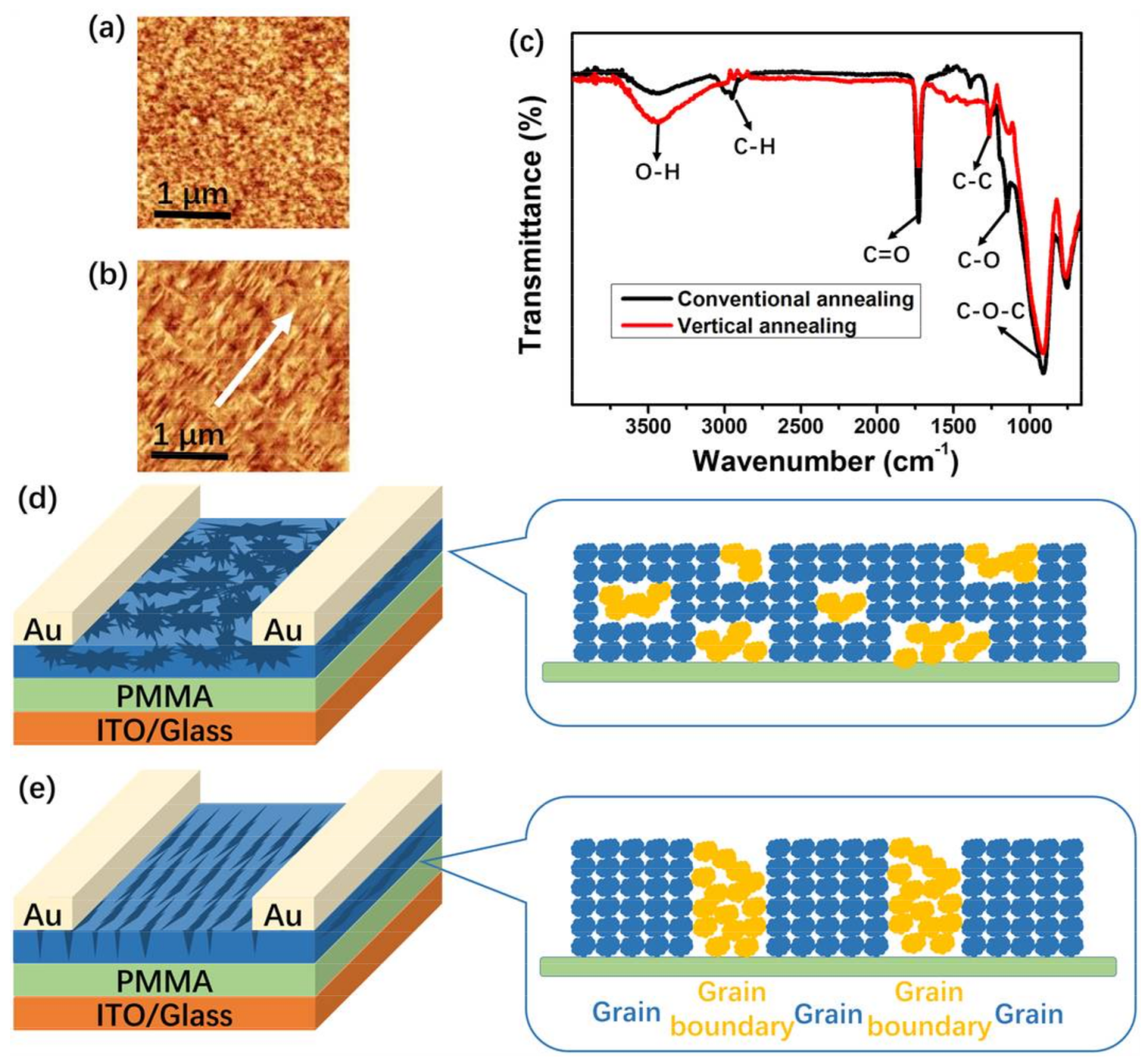
3. Results and Discussion

The electrical performances of OTFTs obtained by the two different annealing methods are firstly investigated. Transfer characteristics of the devices are presented in Figure 2, with a source-drain voltage (VDS) of −40 V. It can be seen that different annealing processes have obviously changed the electrical performances of the OTFTs, including mobility (µ), on-off ratio (Ion/Ioff), threshold voltage (VT), and subthreshold slope (SS), and the detailed electrical parameters of three types of OTFTs are listed in Table 3.
As shown in Table 3, we can see that the parallel device reveals an enhanced µ of 0.0275 cm2/Vs, which is higher than the mobilities of the conventional (0.0186 cm2/Vs) and the perpendicular (0.0092 cm2/Vs) devices. The corresponding saturation current (Ion) are 9.03 µA, 5.79 µA, and 0.61 µA, respectively. Moreover, the parallel and conventional devices have the same Ion/Ioff of about 104, while the Ion/Ioff of the perpendicular device is only about 103. In general, the parallel device shows the best electrical performance, and there is an obvious difference in electrical performance between parallel and perpendicular devices obtained by the same annealing process.
Based on the above improved performance of OTFTs, the gas sensing performance of the devices with conventional annealing and vertical annealing are also characterized by measuring transistor characteristics under programmed NO2 exposure ranging from 1 to 15 ppm. The transfer characteristics of the OTFTs exposed to various concentrations of NO2 are shown in Figure 2. For the transfer curve measurements, all devices were exposed to a specific concentration of NO2 for 2 min before measurement. After introducing strongly oxidizing NO2, some electrons in OSC film will become trapped. Thus, the number of free holes increase, resulting in a reduction of the potential barriers, and an enhancement in the source-drain saturation current [27]. Figure 2a,b show that parallel devices exhibit smaller responses of Ion increasing from 9 µA to 14.7 µA (63%) when exposed to 15 ppm NO2, in contrast to conventional devices which increased from 5.8 µA to 10 µA (72%). However, as shown in Figure 3c, the Ion of the perpendicular device increases significantly from 0.6 µA (0 ppm NO2) to 9.2 µA (15 ppm NO2), yielding a high responsivity of up to 1408%. In order to further understand the effect of different annealing processes on the gas sensing performances of OTFTs, we analyze the sensing performances of conventional and perpendicular devices in detail, including Ion, µ, SS, and VT.
To assess the response R of the OTFT parameters Ion, µ, SS, and VT to different NO2 concentrations we define R = [(RNO2RAIR)/RAIR] × 100%. From the data presented in Figure 3a, it can be seen that Ion of the perpendicular device increased by 1408%, when exposed to 15 ppm NO2. In comparison, the conventional device only increased by 72% under the same concentration of NO2. Accordingly, the perpendicular device shows a greater µ variance rate of 239% in 15 ppm NO2 as compared to 112% of the conventional device. After NO2 exposure, the VT of these two kinds of devices experience only a slight positive shift, while the perpendicular one experiences a much more significant change as shown in Figure 3c. As VT shifts are usually caused by charge trapping at the dielectric/semiconductor interface, more NO2 molecules will trap at the interface and cause more immobilized negative charges to become located there. These localized charges, in turn, will induce more free holes and reduce the negative gate voltage required for the transistor turn-on [30]. Furthermore, as SS is proportional to the trap density at the dielectric/semiconductor interface, the trap density (N) can be extracted by Equation (2) [31,32]:
SS = kT/qln10(1 + qN/C),
where q is the electronic charge, k is Boltzmann’s constant, T is the absolute temperature, and C is the areal capacitance of the dielectric structure. As shown in Figure 3d, the relative change in SS of the two devices decrease in a continuous manner as the NO2 concentration increases. The perpendicular device, in contrast, shows early saturation at fairly small values. We can see that the morphology of the OSC film is effectively affected by the different annealing processes, and that the density of the trap is a key factor determining the NO2 sensing performance.
To elucidate the origin of the different gas sensing performances, AFM was utilized to analyze the morphology of the TIPS-pentacene films grown by conventional and vertical annealing processes. As shown in Figure 4a,b, well-ordered TIPS-pentacene films are formed on PMMA dielectrics by vertical annealing as compared to the irregular grains formed by conventional annealing. Furthermore, the similar FTIR spectra in Figure 4c indicate that there is almost no change in the chemical characteristics of the TIPS-pentacene films formed by two different annealing methods. Thus, well-aligned TIPS-pentacene films formed by vertical annealing are the major factor on the enhancement of NO2 sensing performance. Due to the well-aligned TIPS-pentacene films, the conductivity of active layers is highly anisotropic [33]. When the grain orientation of the OSC films is perpendicular to the conducting channel, charge carriers pass through a larger number of grain boundaries on their journey from source to drain electrodes than in a conventional device. In the band bending model, grain boundaries are represented by depletion regions, and the holes transfer via hopping from one grain to another [24,34]. This is in good agreement with the above phenomenon that perpendicular devices show a lower µ compared to conventional ones. Moreover, as illustrated in Figure 4d,e, in conventional device consisting of disordered TIPS-pentacene grains, charge carriers in the first monolayer are able to move through grains in the second layer, which short-circuit the grain boundaries in the first layer. In this way, grain boundaries become less important to charge transport, and the signals produced by the interaction of NO2 with these grain boundaries will not be shown in source-drain saturation current. In contrast, when moving in well-aligned TIPS-pentacene grains in vertical devices, charge carriers are inevitably forced into grain boundaries which cannot be bypassed through upper grains, thus resulting in larger grain boundary effects and a larger NO2 responsivity [35,36].
Furthermore, real-time responsivities were tested for three devices biased at VDS = VGS = −40 V, responding to the dynamic switching to different concentrations of NO2 (1, 2, 5, 10, and 15 ppm) at room temperature. Prior to each device test, the IDS of all devices was allowed to reach a steady state after 30 min in dry air. From the test results shown in Figure 5, it is obvious that the sensing performance of the perpendicular device is superior to an OTFT formed by conventional annealing. When exposed to 15 ppm NO2 for 10 min, the IDS charges in the conventional and perpendicular devices are 93% and 1235%, respectively. Compared to the conventional device, the perpendicular device shows a one-order-of-magnitude improvement in NO2 sensing performance. These results are in agreement with the previous results. Thus, the increased number of effective grain boundaries can effectively improve the NO2 sensing performance of OTFTs. The responses of conventional and parallel devices to NO2 pulses were also studied, and the obtained curves are shown in Figure S1 (Supplementary Materials). In addition, the perpendicular device shows a high responsivity of 539% already at a concentration of 1 ppm, which indicates that the vertical device offers great potential for becoming low-concentration detectors for NO2. Subsequently, the responses of conventional and perpendicular devices to lower concentration of NO2 (200, 400, 800 ppb) were tested (Figure S2, Supplementary Materials). The results exhibit that the perpendicular device also shows a greater response than the conventional device.
Selectivity is a crucial parameter for practical sensing applications, which usually relies on the specific interaction between the organic semiconductors and the analytes. To probe the selectivity of the device, we measured the responses of the perpendicular device to several other common gases, including SO2 as an oxidizing gas and NH3, CO, and H2S as reducing gases. All these gases are separately mixed with dry air to form a fixed concentration of 15 ppm. As shown in Figure 6, the perpendicular device presents a specifically preferential response to NO2, while no obvious responses are observed with 15 ppm SO2. The possible reason might be that NO2 is more strongly oxidizing on TIPS-pentacene than SO2 [37]. For the reducing gases of NH3, CO, and H2S, the saturation currents decrease with a decrement of −52%, −24%, and −77%, respectively. As a consequence, the other gases may be have weaker chemical interaction with TIPS-pentacene, resulting in a high responsivity to NO2.

4. Conclusions

In summary, a simple vertical annealing process was proposed for the fabrication of high-performance OTFT based NO2 sensors. The NO2 responsivity of OTFT based sensors improved one order of magnitude from 72% to 1408%, relative to conventionally prepared devices. The sensing performance enhancement is due to the superior alignment of TIPS-pentacene film caused by the vertical annealing process. In this way, a large number of effective grain boundaries in the conducting channel could be obtained, resulting in an improvement in the gas sensing performance. Moreover, gas sensors formed by vertical annealing achieved a high sensing performance of 589% already at 1 ppm NO2, showing at the same time a preferential response to NO2. The method of vertical annealing, demonstrated in this work, not only opens an effective way for the improvement of OTFT gas sensing performance, but also offers great potential for low-cost, fast, and portable electronic noses.

Supplementary Materials

The following are available online at https://www.mdpi.com/2079-4991/8/4/203/s1, Figure S1: Response curves of the conventional and parallel device to NO2 pulses, Figure S2: Response curves of conventional and perpendicular devices to low concentration NO2 pulses.

Acknowledgments

The authors gratefully acknowledge the financial support from the Foundation for Innovation Research Groups of National Natural Science Foundation of China (NSFC) (grant no. 61421002), the Foundation of NSFC (grant: no. 61675041 & 51703019), and Science and Technology Department of Sichuan Province (grant: no. 2016HH0027 & 2016FZ0100).

Author Contributions

Sihui Hou and Xinming Zhuang conceived and designed the experiments; Sihui Hou and Zuchong Yang performed the experiments; Xinming Zhuang, Zuchong Yang and Junsheng Yu provided valuable suggestions; and Sihui Hou wrote the paper.

Conflicts of Interest

The authors declare no conflict of interest.

References

  1. Huang, W.; Zhuang, X.; Melkonyan, F.S.; Wang, B.; Zeng, L.; Wang, G.; Han, S.; Bedzyk, M.J.; Yu, J.; Marks, A.; et al. UV-Ozone interfacial modification in organic transistors for high-sensitivity NO2 detection. Adv. Mater. 2017, 29, 1701706. [Google Scholar] [CrossRef] [PubMed]
  2. Nejat, P.; Jomehzadeh, F.; Taheri, M.M.; Gohari, M.; Abd Majid, M.Z. A global review of energy consumption, CO2 emissions and policy in the residential sector (with an overview of the top ten CO2 emitting countries). Renew. Sustain. Energ. Rev. 2015, 43, 843–862. [Google Scholar] [CrossRef]
  3. Guo, Y.; Yu, G.; Liu, Y. Functional organic field-effect transistors. Adv. Mater. 2010, 22, 4427–4447. [Google Scholar] [CrossRef] [PubMed]
  4. Zang, Y.; Huang, D.; Di, C.A.; Zhu, D. Device engineered organic transistors for flexible sensing applications. Adv. Mater. 2016, 28, 4549–4555. [Google Scholar] [CrossRef]
  5. Qian, C.; Sun, J.; Kong, L.A.; Gou, G.; Zhu, M.; Yuan, Y.; Huang, H.; Gao, Y.; Yang, J. High-performance organic heterojunction phototransistors based on highly ordered copper phthalocyanine/para-sexiphenyl thin films. Adv. Funct. Mater. 2017, 27, 1604933. [Google Scholar] [CrossRef]
  6. Baeg, K.J.; Caironi, M.; Noh, Y.Y. Toward printed integrated circuits based on unipolar or ambipolar polymer semiconductors. Adv. Mater. 2013, 25, 4210–4244. [Google Scholar] [CrossRef] [PubMed]
  7. Wu, X.; Mao, S.; Chen, J.; Huang, J. Strategies for improving the performance of sensors based on organic field-effect transistors. Adv. Mater. 2018. [Google Scholar] [CrossRef] [PubMed]
  8. Hodgkinson, J.; Tatam, R.P. Optical gas sensing: A review. Meas. Sci. Technol. 2013, 24, 012004. [Google Scholar] [CrossRef]
  9. Huang, Z.F.; Song, J.; Pan, L.; Zhang, X.; Wang, L.; Zou, J.J. Tungsten oxides for photocatalysis, electrochemistry, and phototherapy. Adv. Mater. 2015, 27, 5309–5327. [Google Scholar] [CrossRef] [PubMed]
  10. Kumar, P.; Morawska, L.; Martani, C.; Biskos, G.; Neophytou, M.; Di Sabatino, S.; Bell, M.; Norford, L.; Britter, R. The rise of low-cost sensing for managing air pollution in cities. Environ. Int. 2015, 75, 199–205. [Google Scholar] [CrossRef] [PubMed] [Green Version]
  11. Smulko, J.M.; Trawka, M.; Granqvist, C.G.; Ionescu, R.; Annanouch, F.; Llobet, E.; Kish, L.B. New approaches for improving selectivity and sensitivity of resistive gas sensors: A review. Sensor Rev. 2015, 35, 340–347. [Google Scholar] [CrossRef]
  12. Trung, T.Q.; Tien, N.T.; Seol, Y.G.; Lee, N.E. Transparent and flexible organic field-effect transistor for multi-modal sensing. Org. Electron. 2012, 13, 533–540. [Google Scholar] [CrossRef]
  13. Han, S.; Zhuang, X.; Jiang, Y.; Yang, X.; Li, L.; Yu, J. Poly(vinyl alcohol) as a gas accumulation layer for an organic field-effect transistor ammonia sensor. Sens. Actuator B Chem. 2017, 243, 1248–1254. [Google Scholar] [CrossRef]
  14. Zhang, X.; Jie, J.; Deng, W.; Shang, Q.; Wang, J.; Wang, H.; Chen, X.; Zhang, X. Alignment and patterning of ordered small-molecule organic semiconductor micro-/nanocrystals for device applications. Adv. Mater. 2016, 28, 2475–2503. [Google Scholar] [CrossRef] [PubMed]
  15. Wang, B.; Zhu, T.; Huang, L.; Tam, T.L.D.; Cui, Z.; Ding, J.; Chi, L. Addressable growth of oriented organic semiconductor ultra-thin films on hydrophobic surface by direct dip-coating. Org. Electron. 2015, 24, 170–175. [Google Scholar] [CrossRef]
  16. Su, Y.; Gao, X.; Liu, J.; Xing, R.; Han, Y. Uniaxial alignment of triisopropylsilylethynyl pentacene via zone-casting technique. Phys. Chem. Chem. Phys. 2013, 15, 14396–14404. [Google Scholar] [CrossRef] [PubMed]
  17. Van Tho, L.; Park, W.T.; Choi, E.Y.; Noh, Y.Y. Highly aligned conjugated polymer films prepared by rotation coating for high-performance organic field-effect transistors. Appl. Phys. Lett. 2017, 110, 163303. [Google Scholar] [CrossRef]
  18. Nam, S.; Jeong, Y.J.; Jung, J.; Kim, S.H.; Ahn, J.; Shin, K.; Jang, J. Direct printing of soluble acene crystal stripes by a programmed dip-coating process for organic field-effect transistor applications. J. Mater. Chem. C 2018, 6, 799–807. [Google Scholar] [CrossRef]
  19. Niazi, M.R.; Li, R.; Qiang Li, E.; Kirmani, A.R.; Abdelsamie, M.; Wang, Q.; Pan, W.; Payne, M.M.; Anthony, J.E.; Smilgies, D.M.; et al. Solution-printed organic semiconductor blends exhibiting transport properties on par with single crystals. Nat. Commun. 2015, 6, 8598–8607. [Google Scholar] [CrossRef] [PubMed]
  20. Lin, F.J.; Guo, C.; Chuang, W.T.; Wang, C.L.; Wang, Q.; Liu, H.; Hsu, C.S.; Jiang, L. Directional solution coating by the chinese brush: A facile approach to improving molecular alignment for high-performance polymer TFTs. Adv. Mater. 2017, 29, 1606987. [Google Scholar] [CrossRef] [PubMed]
  21. Janneck, R.; Vercesi, F.; Heremans, P.; Genoe, J.; Rolin, C. Predictive model for the meniscus-guided coating of high-quality organic single-crystalline thin films. Adv. Mater. 2016, 28, 8007–8013. [Google Scholar] [CrossRef] [PubMed]
  22. Bharti, D.; Raghuwanshi, V.; Varun, I.; Mahato, A.K.; Tiwari, S.P. Directional solvent vapor annealing for crystal alignment in solution-processed organic semiconductors. ACS Appl. Mater. Interfaces 2017, 9, 26226–26233. [Google Scholar] [CrossRef] [PubMed]
  23. Keum, C.M.; Bae, J.H.; Kim, M.H.; Park, H.L.; Payne, M.M.; Anthony, J.E.; Lee, S.D. Topography-guided spreading and drying of 6,13-bis(triisopropylsilylethynyl)-pentacene solution on a polymer insulator for the field-effect mobility enhancement. Appl. Phys. Lett. 2013, 102, 193307. [Google Scholar] [CrossRef]
  24. Li, Y.; Ji, D.; Liu, J.; Yao, Y.; Fu, X.; Zhu, W.; Xu, C.; Dong, H.; Li, J.; Hu, W. Quick fabrication of large-area organic semiconductor single crystal arrays with a rapid annealing self-solution-shearing method. Sci. Rep. 2015, 5, 13195. [Google Scholar] [CrossRef] [PubMed]
  25. Li, L.; Gao, P.; Baumgarten, M.; Mullen, K.; Lu, N.; Fuchs, H.; Chi, L. High performance field-effect ammonia sensors based on a structured ultrathin organic semiconductor film. Adv. Mater. 2013, 25, 3419–3425. [Google Scholar] [CrossRef] [PubMed]
  26. Wang, B.; Ding, J.; Zhu, T.; Huang, W.; Cui, Z.; Chen, J.; Huang, L.; Chi, L. Fast patterning of oriented organic microstripes for field-effect ammonia gas sensors. Nanoscale 2016, 8, 3954–3961. [Google Scholar] [CrossRef] [PubMed]
  27. Shi, W.; Yu, X.; Zheng, Y.; Yu, J. DNA based chemical sensor for the detection of nitrogen dioxide enabled by organic field-effect transistor. Sens. Actuator B Chem. 2016, 222, 1003–1011. [Google Scholar] [CrossRef]
  28. Wang, Z.; Huang, L.; Zhu, X.; Zhou, X.; Chi, L. An ultrasensitive organic semiconductor NO2 sensor based on crystalline TIPS-pentacene films. Adv. Mater. 2017, 29, 1703192. [Google Scholar] [CrossRef] [PubMed]
  29. Hsu, M.H.; Chang, S.P.; Chang, S.J.; Wu, W.T.; Li, J.Y. Oxygen partial pressure impact on characteristics of indium titanium zinc oxide thin film transistor fabricated via RF sputtering. Nanomaterials 2017, 7, 156. [Google Scholar] [CrossRef] [PubMed]
  30. Zhuang, X.; Huang, W.; Yang, X.; Han, S.; Li, L.; Yu, J. Biocompatible/degradable silk fibroin:poly(vinyl alcohol)-blended dielectric layer towards high-performance organic field-effect transistor. Nanoscale Res. Lett. 2016, 11, 439–446. [Google Scholar] [CrossRef] [PubMed]
  31. Zhuang, X.; Huang, W.; Han, S.; Jiang, Y.; Zheng, H.; Yu, J. Interfacial modifying layer-driven high-performance organic thin-film transistors and their nitrogen dioxide gas sensors. Org. Electron. 2017, 49, 334–339. [Google Scholar] [CrossRef]
  32. Shi, W.; Zheng, Y.; Taylor, A.D.; Yu, J.; Katz, H.E. Increased mobility and on/off ratio in organic field-effect transistors using low-cost guanine-pentacene multilayers. Appl. Phys. Lett. 2017, 111, 043301. [Google Scholar] [CrossRef]
  33. Pitsalidis, C.; Kalfagiannis, N.; Hastas, N.A.; Karagiannidis, P.G.; Kapnopoulos, C.; Ioakeimidis, A.; Logothetidis, S. High performance transistors based on the controlled growth of triisopropylsilylethynyl-pentacene crystals via non-isotropic solvent evaporation. RSC Adv. 2014, 4, 20804–20813. [Google Scholar] [CrossRef]
  34. Andringa, A.M.; Christian Roelofs, W.S.; Sommer, M.; Thelakkat, M.; Kemerink, M.; de Leeuw, D.M. Localizing trapped charge carriers in NO2 sensors based on organic field-effect transistors. Appl. Phys. Lett. 2012, 101, 153302. [Google Scholar] [CrossRef]
  35. Wang, J.; Jiang, C. Electrical transport mechanism of single monolayer pentacene film employing field-effect characterization. Org. Electron. 2015, 16, 164–170. [Google Scholar] [CrossRef]
  36. Mirza, M.; Wang, J.; Wang, L.; He, J.; Jiang, C. Response enhancement mechanism of NO2 gas sensing in ultrathin pentacene field-effect transistors. Org. Electron. 2015, 24, 96–100. [Google Scholar] [CrossRef]
  37. Han, S.; Zhuang, X.; Shi, W.; Yang, X.; Li, L.; Yu, J. Poly(3-hexylthiophene)/polystyrene (P3HT/PS) blends based organic field-effect transistor ammonia gas sensor. Sens. Actuator B Chem. 2016, 225, 10–15. [Google Scholar] [CrossRef]
Figure 1. Device architecture of the OTFTs used in this study (a). Molecular structures of PMMA (b) and TIPS-pentacene (c). Schematic of OTFT subjected to different annealing processes (d).
Nanomaterials 08 00203 g001
Figure 2. (ac) Transfer characteristics curves of OTFTs obtained by two different annealing methods. Transfer curves (df) of OTFT sensors obtained by different annealing methods under a specific concentration of NO2 (VDS = −40 V).
Nanomaterials 08 00203 g002
Figure 3. Variation of Ion (a), µ (b), VT (c), and SS (d) of OTFTs at different NO2 concentrations.
Nanomaterials 08 00203 g003
Figure 4. AFM topography images of TIPS-pentacene films of conventional device (a) and the perpendicular device (b). FTIR spectra of TIPS-pentacene films with the PMMA dielectric formed by conventional and vertical annealing methods (c). Schematic diagrams of crystallization orientation of parallel device (d) and the perpendicular device (e).
Nanomaterials 08 00203 g004
Figure 5. Response curves of conventional and perpendicular devices to NO2 pulses.
Nanomaterials 08 00203 g005
Figure 6. Drain current changes for perpendicular device exposed to different gases.
Nanomaterials 08 00203 g006
Table 1. Properties of some common used gas sensors.
Test MethodSensitivitySelectivityResponse SpeedCostDetection RangeRef.
OTFTsexcellentgoodgreatlowppb[4,5,6,7]
Infrared Absorptiongreatgoodgoodcommonwide[8]
Photochemistrygreatgreatgreatcommonppm[9]
Chromatographyexcellentexcellentexcellentexpensiveppm[10]
Resistiveexcellentgoodgoodlowppm[11]
Table 2. Recently-reported processes to obtain ordered active layers.
AuthorTechniqueSemiconductorSolventMobility (cm2 V−1 s−1)Ref.
SuZone castingTIPS-pentaceneChloroform0.67[16]
Van ThoRotation coatingDPPT-TTDCB1.95[17]
NamDip coatingTIPS-pentaceneDCM0.24[18]
NiaziBlade coatingdiF-TES-ADTtoluene6.70[19]
LinBrush coatingDPPDTTDCB11.20[20]
JanneckMeniscus-guided coatingC8-BTBTheptane7.00[21]
Table 3. Field-effect mobility (µ), current on-off ratio (Ion/Ioff), threshold voltage (VT), and subthreshold slope (SS) of different OTFTs.
Deviceµ (cm2/Vs)Ion/IoffVT (V)SS (V/dec)
Conventional device0.0186~104−2.42.0
Parallel device0.0275~104−2.01.8
Perpendicular device0.0092~103−20.06.8

