Article

Charge Transfer Tuned by the Surrounding Dielectrics in TiO2-Ag Composite Arrays

1
School of Chemistry and Chemical Engineering, Jiangsu University, Zhenjiang 212013, China
2
Zhonggong Education and Technology Co., Ltd., Changchun 130000, China
3
College of Materials and Environmental Engineering, Hangzhou Dianzi University, Hangzhou 310018, China
*
Authors to whom correspondence should be addressed.
Nanomaterials 2018, 8(12), 1019; https://doi.org/10.3390/nano8121019
Submission received: 10 November 2018 / Revised: 27 November 2018 / Accepted: 4 December 2018 / Published: 7 December 2018

Abstract

:
TiO2/Ag bilayer films sputtered onto a 2D polystyrene (PS) bead array in a magnetron sputtering system were found to form a nanocap-shaped nanostructure composed of a TiO2-Ag composite on each PS bead, in which the Ag nanoparticles were trapped partially or fully in the TiO2 matrix, depending on the TiO2 thickness. X-ray Photoelectron Spectroscopy (XPS) results showed the opposite shifts of binding energy for Ti 2p and Ag 3d, indicating the transfer of electrons from metallic Ag to TiO2 owing to the Ag-O-TiO2 composite formation. UV-Vis absorption spectra showed the blue shifts of the surface plasma resonance peaks, and the maximum absorption peak intensity was obtained for TiO2 at 30 nm. The surface-enhanced Raman scattering (SERS) peak intensity first increased and then decreased when the TiO2 thickness changed. The observations of SERS, XPS, and UV-Vis absorption spectra were explained by the dependency of the charge-transfer process on TiO2 thickness, which was ascribed to the changing dielectric properties in the metal/semiconductor system.

1. Introduction

When excited by a light incident on a metal surface, free electrons show a collective oscillation, known as surface plasma [1]. Surface plasma in nanostructures leads to an enhanced local electromagnetic field, which has excellent applications in many fields such as biomolecule analysis, pollution material degradation, energy conversion, and surface-enhanced Raman scattering (SERS) [2,3,4,5,6]. In these studies, the noble metals Au and Ag have been widely investigated due to their unique plasma characteristics, however, their applications are largely limited by shortcomings such as high cost, poor stability, and no reusability. To overcome these shortcomings, photocatalytic self-cleaning materials have recently been developed by combining plasmonic metal with conventional semiconductor photocatalysts such as TiO2 [7,8,9,10] and ZnO [11], which makes the materials recyclable to reduce the potential cost. TiO2 is an excellent photocatalyst material due to its good physical and chemical stability and high photocatalytic activity [12,13,14]. However, the quantum efficiency of TiO2 is greatly limited due to its quick recombination of photogenerated electrons and holes [15]. One main approach to improving the efficiency of such materials is the addition of nanoparticles to the titanium surface, which can trap electrons and lessen the recombination of electron-hole pairs [16,17]. TiO2 modified with Ag has been proven to restrain the recombination of photo-excited electrons and holes, which can improve the photocatalytic performance [18]. In our recent work, nanocap arrays of TiO2/Ag and co-sputtering TiO2-Ag were fabricated on two-dimensional colloidal arrays [19]. A significant SERS enhancement was observed when the sublayer Ag was 10 nm compared to the pure Ag monolayer, which is mainly ascribed to the charge–transfer effect.
Since the charge–transfer process depends on the surrounding dielectric properties, the charge–transfer behavior can be tailored by the materials around the metals. In this paper, we prepare a composite TiO2-Ag array on 2D polystyrene (PS) colloidal spheres. TEM measurements show Ag nanoparticles embedded in the semiconductor TiO2 matrix. When the TiO2 thickness changes, the morphology of each unit changes from partially-trapped Ag nanoparticles to fully-trapped Ag nanoparticles in the TiO2 matrix. XPS, SERS, and UV-Vis absorption spectra measurements indicated the charge–transfer process in our TiO2-Ag composite, which was attributed to the change in the surrounding dielectrics.

2. Experimental Section

2.1. Materials

The probing molecules are 4-Aminothiophenol (PATP) and Methylene blue (MB), with a purity of 99.9%. Sodium dodecyl sulfate and ethanol were purchased from Sigma Aldrich (St., Louis, MO, USA). The polystyrene (PS) colloidal beads were purchased from The Duke Co., Ltd., (Palo Alto, CA, USA) with a concentration of 10 wt % and a particle deviation less than 10%. Ag and TiO2 targets were supplied by Beijing TIANRY Science and Technology Developing Center (Beijing, China), with a purity 99.99% (wt %). Silicon wafers were supplied by Hefei Kejing Materials Technology Co., Ltd. (Hefei, China).

2.2. Preparation and Characterization

The film was deposited in a magnetron sputtering system model JGP-560C (Shenyang, China), with a base vacuum of 2 × 10⁻⁴ Pa and an argon pressure of 0.6 Pa. The sputtering power 50 W was applied to the target TiO2 and the sputtering power 21.6 W was applied to the target Ag. A PS (200 nm) monolayer was assembled on a modified Si substrate. First, the PS colloidal solution and ethanol were mixed with the same volume ultrasonically. The Si substrate covered with the mixture was submerged in water. The PS monolayer formed on the water surface, which was picked up by a new Si substrate. The ion beam etch technique was used to separate the PS beads from each other, using 2000 eV of energy and an etching time of 300 s. To realize saturation adsorption, the samples were immersed in PATP (3%) for more than 30 min. The morphology and microstructure measurements were performed by field emission scanning electron microscopy (FESEM) under an accelerating voltage of 5.0 KV and transmission electron microscopy (TEM) on JEM-2100HR (JEOL, Tokyo, Japan). UV-Vis spectra were obtained on a spectrophotometer, model Shimadzu UV-3600 (Kyoto, Japan). X-ray photoelectron spectroscopy was carried out by the Thermo Fisher Scientific (Waltham, MA, USA) system to determine the elemental composition and chemical state. Raman spectra were obtained with a Renishaw Raman (London, UK) system model 2000 confocal microscopy spectrometer with a spectral resolution of 1 cm−1. An air-cooled argon ion laser with 514.5 nm radiation (40 mW, power out of 1%) was used for the SERS. The spectra were recorded with an accumulation time of 10 s.

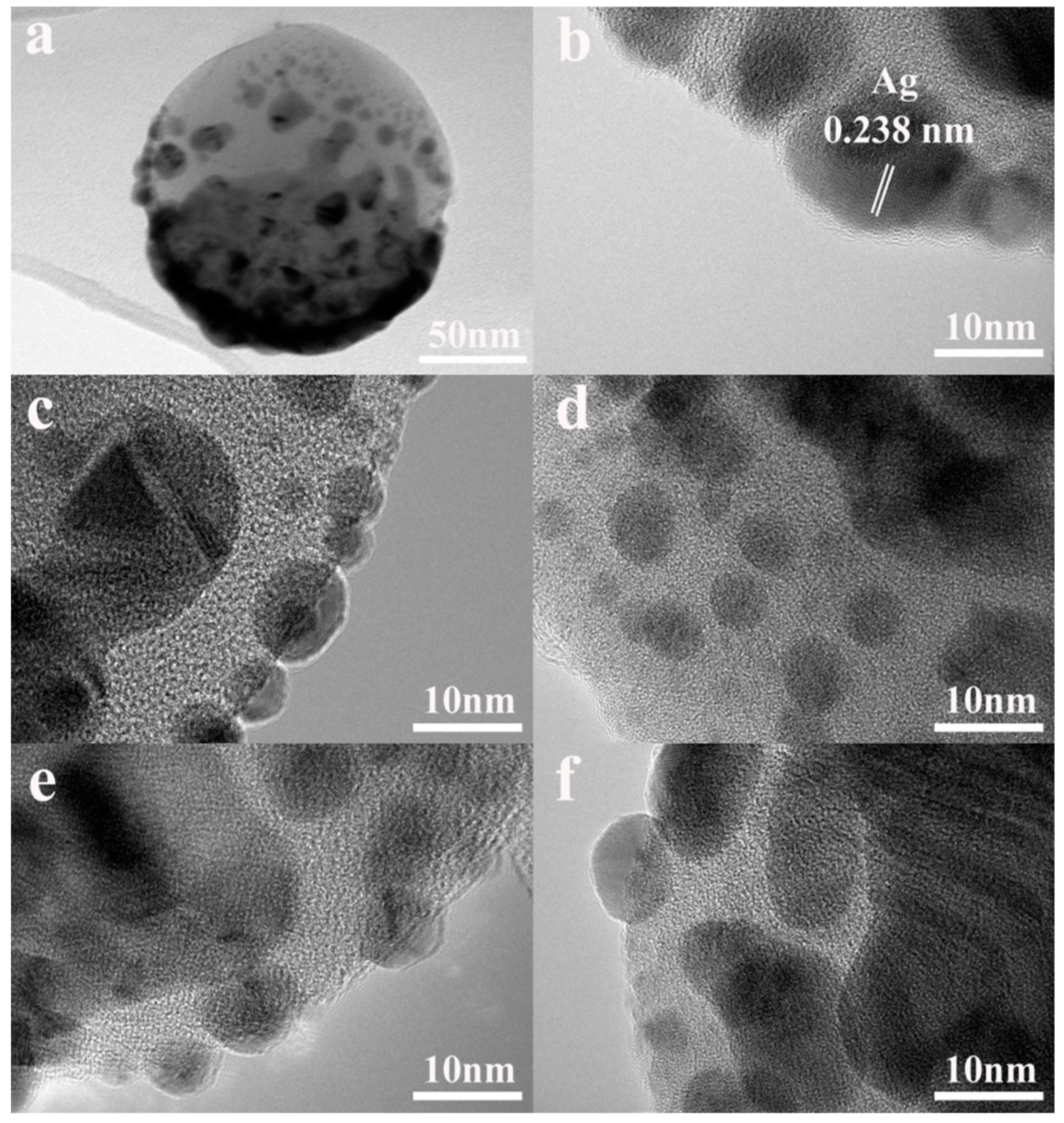
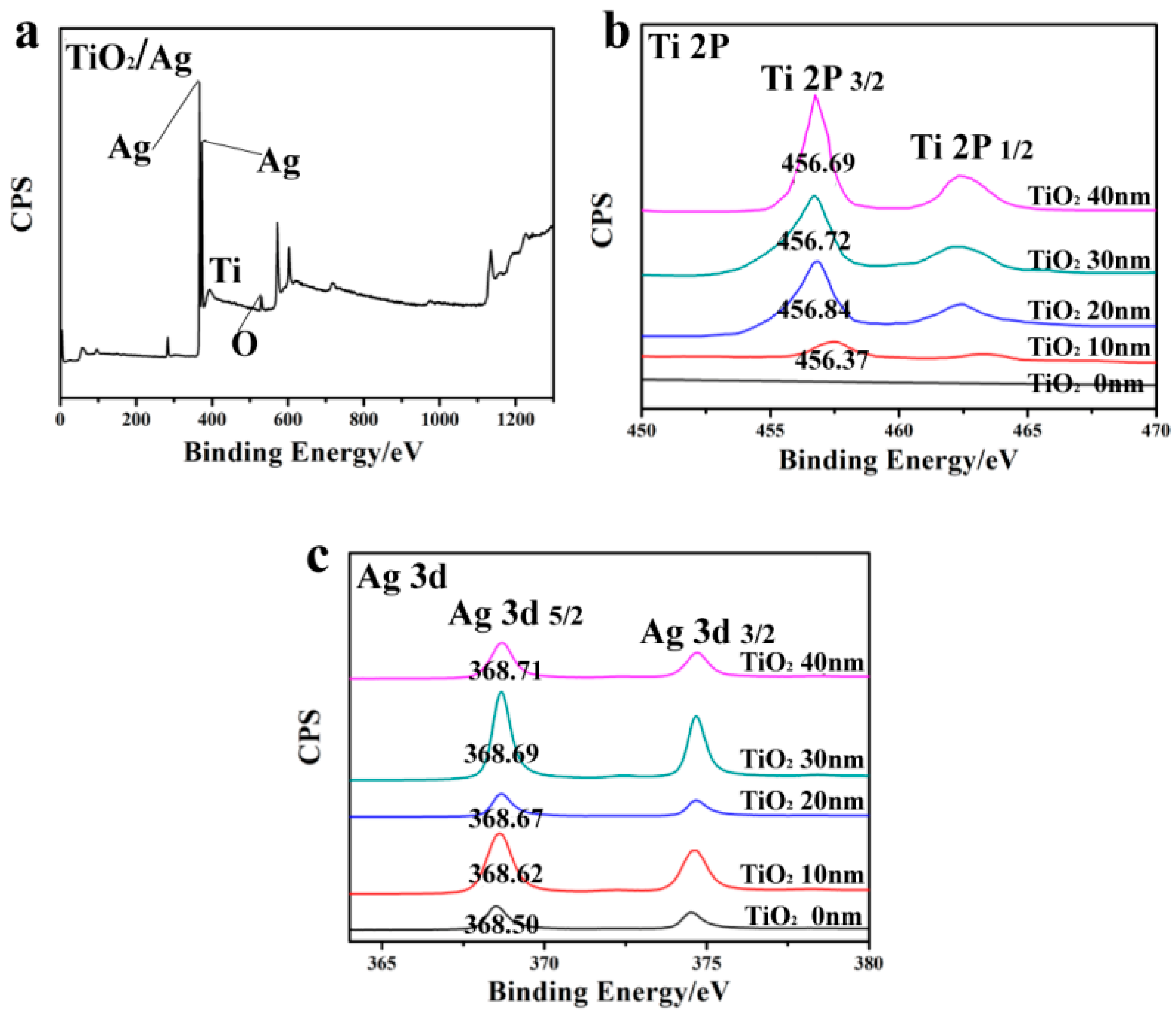
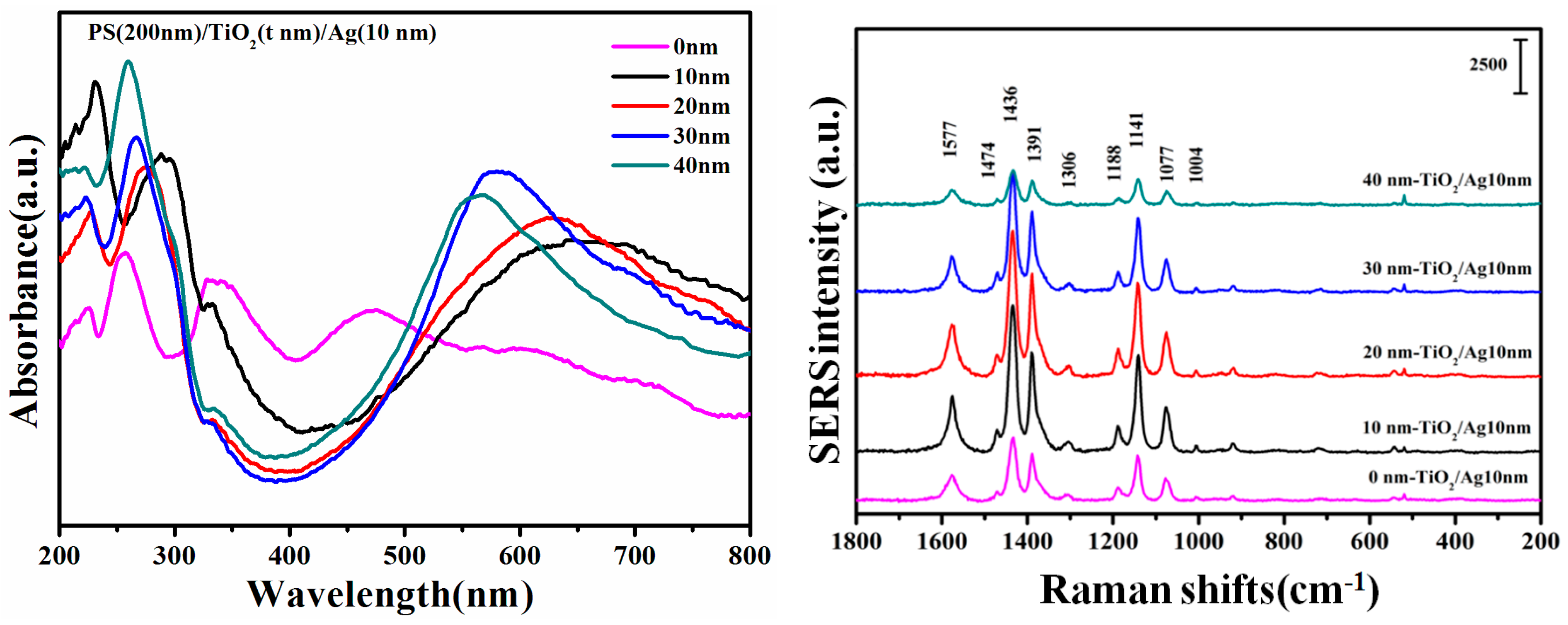
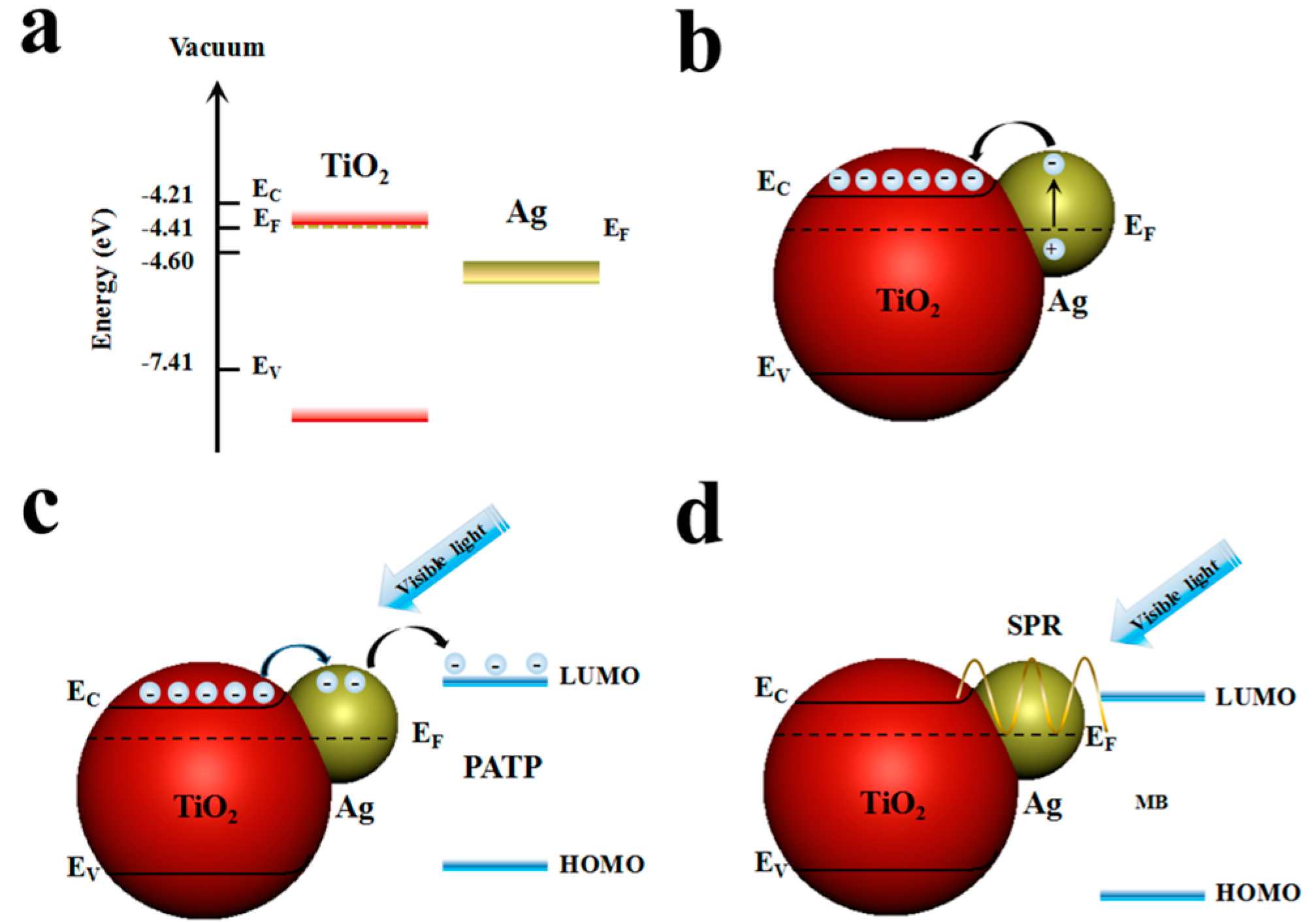
3. Results and Discussion

Figure 1 shows the schematic for fabrication as well as the FESEM images of the nanocaps TiO2 (t nm)/Ag 10 nm (t = 10 nm, 20 nm, 30 nm, 40 nm). The PS beads were isolated from each other. When the TiO2/Ag film was deposited onto the PS beads, the isolated TiO2/Ag cap formed on each PS bead without connection with the neighbors, as the film thickness was far smaller than the bead radius. The aggregations of Ag particles become obvious and the surface roughness increased as the TiO2 thickness increased from 10 nm to 40 nm.
The HRTEM images showed that TiO2 was amorphous and the spherical Ag particles with sizes between 5 nm and 10 nm were dispersed in the amorphous TiO2 matrix. Some Ag nanoparticles were partially or fully embedded in the TiO2 matrix and some remained on the surface, which led to the significantly rough surfaces (Figure 2b). When the TiO2 thickness increased, the ratio of Ag nanoparticles embedded in the TiO2 matrix increased and the size of the Ag nanoparticles also increased. When the Ag target was sputtered in the magnetic control system, it was difficult to form a continuous layer with an Ag thickness below 10 nm and many defects and holes formed in the film. Some high-energy Ag nanoparticles were able to penetrate into the TiO2 layer, forming a mixture structure with Ag nanoparticles fully-embedded or partially-embedded in the TiO2 matrix. When the TiO2 layer thickness further increased, the number of defects and holes decreased in the TiO2 layer and the diffusion barrier energy increased, which limited the diffusion of Ag and led to the growth of Ag particles.
XPS measurements were carried out to identify the element composition of TiO2-Ag and analyze the chemical status of the elements. The survey XPS spectrum in Figure 3a shows the existence of Ti, Ag, and O elements in TiO2-Ag nanocaps, and the high-resolution XPS spectra of Ti 2p and Ag 3d are shown in Figure 3b,c. The Ti 2P spectrum consisted of two peaks identified as Ti 2P3/2 and Ti 2P1/2, respectively (Figure 3b). The binding energy of Ti moved in the direction of low binding energy when the TiO2 thickness increased, which suggested an increasing electron density for accepting some electrons. The peaks of Ag 3d5/2 and Ag 3d3/2 moved slightly towards the high binding energy (Figure 3c), which shows that the Ag lost some electrons and that the electron density decreased. The opposite shifts of binding energy for Ti 2p and Ag 3d indicated that some electrons transferred from metallic Ag to TiO2 owing to the interactions between the metal Ag and the semiconductor TiO2 [20]. However, in the Ag 3d spectra, the splitting of the Ag 3d binding energy was 6.0 eV, which indicated that the Ag mainly showed the Ag0 state in the TiO2-Ag nanocap structure, without the obvious oxidation of Ag. In this case, it is probable that the Ag nanoparticles part-embedded in the TiO2 matrix induced the formation of an Ag-O-Ti composite at the junction of TiO2 and Ag, which promoted the electron transfer from the surface of the Ag nanoparticle to the TiO2 [21].
Compared to pure Ag, the TiO2-Ag nanocaps exhibited strong absorption in the UV and visible region, as shown in Figure 4. The absorption peaks of the Ag film at about 340 nm and 460 nm came from dipole resonance and quadrupole resonance, which broadened due to the coupling between the quadrupole resonance and the octupole resonance [22]. As the small Ag nanoparticles were almost trapped inside the TiO2 matrix and there was no exposure to oxygen, the excited electrons transferring from the surface of the Ag nanoparticle to the TiO2 conduction band remained in the Ag-TiO2 complex, leading to the increased concentration of free conduction electrons, which broadened the absorption band of the Ag-TiO2 complex. When the TiO2 thickness changed from 10 nm to 40 nm, the blue shifts of the resonance peaks were observed from 630 nm to 560 nm and became narrow. The absorption peak intensity first increased and then decreased, and the maximum was obtained when the TiO2 was 30 nm. With the increase of TiO2 thickness from 10 nm to 30 nm, more Ag nanoparticles were encaged in the TiO2 host matrix and began to agglomerate into large particles, which made the absorption peak narrow. When the TiO2 thickness increased to 40 nm, the absorption peak began to decrease, which may be attributed to the depressed plasmon absorption by TiO2. The observed blue shift was mainly because of the dielectric properties of the surrounding TiO2 and the interfacial electron transfer between Ag nanoparticles and TiO2. The Schottky barrier formed in the metal–semiconductor contact region due to the transfer of electrons from Ag to TiO2, which reduced the recombination rate of the electron-hole and improved the separation efficiency of the electron–hole pairs leading to the blue shift, consistent with the XPS results.
The SERS activities of the TiO2/Ag nanocap arrays were evaluated by the probe molecules 4-Aminothiophenol (PATP). The PATP molecules showed characteristic peaks located at 1004, 1077, 1141, 1188, 1306, 1391, 1436, 1474, and 1577 cm−1. Of these peaks, the peaks at 1077, 1188, and 1474 cm−1 were assigned to the ν(C-S), δ(C-H), and ν(C-C) stretching vibration, respectively, which were dominated by characteristic a1 vibrational modes [23,24,25]. The δ(C-H) at 1141 cm−1, [ν(C-C) + δ(C-H)] at 1391 and 1436 cm−1, and ν(C-C) at 1577 cm−1 were interpreted as b2 modes, as shown in Table 1 [26,27,28]. For pure Ag, the enhanced peaks were believed to be due to the roughness of the nanocap caused by Ag nanoparticles. However, decreases in the SERS intensity, for thicker TiO2 with 30 nm and 40 nm, were mainly caused by the reduced surface plasmon due to the embedment of the Ag nanoparticles in TiO2.
The SERS peak intensity first increased and then decreased when the TiO2 thickness changed from 0 to 40 nm. The charge-transfer (CT) process between the molecule and the TiO2/Ag substrate may play an important role in the change of SERS intensity. The degree of charge–transfer is used to evaluate the contribution of the chemical mechanism (CM) to the SERS intensity [29,30]. In the TiO2/Ag system, the peaks at 1077 cm−1 and 1436 cm−1 were chosen for CM analysis. The band at 1077 cm−1 is for the C-S stretching mode (a1 mode), which is totally symmetric to the SERS signal contributions. The other peak, 1436 cm−1 (b2 mode) is non-totally symmetric, because the adsorption effect and the SERS effect are affected by the CT process.
According to the CT mechanism, non-vibration modes such as the b2 mode, are usually enhanced by the Herzberg–Teller contribution of CT, whereas the a1 model was not affected by the contribution of CT. In this case, changes in the CT process caused by various CM effects were qualitatively analyzed by PCT. The values of the degree of charge–transfer first increased from 0.693, to 0.746, 0.748, and then to 0.759, followed by a decrease to 0.751 when the TiO2 thickness was 0 nm, 10 nm, 20 nm, 30 nm, and 40 nm, which indicates the charge transition from the Fermi level of the TiO2/Ag composites to the lowest unoccupied molecular orbitals (LUMO) of the PATP molecules, as shown in Figure 5 [31].

4. Conclusions

In summary, a thin film of Ag was sputtered onto the TiO2 layer of different thicknesses to form the structure with Ag nanoparticles embedded in the TiO2 layer. The XPS peaks of Ti and Ag moved in opposite directions, indicating the changed electron density between the TiO2 and Ag, which in turn indicates the promotion of the electron transfer from the surface of the Ag nanoparticle to the TiO2 through the formation of the Ag-O-Ti composite. When TiO2 thickness changed from 10 nm to 40 nm, the UV spectra showed the blue shift resonance peaks from 630 nm to 560 nm and the maximum absorption peak intensity was obtained for the TiO2, namely 30 nm, due the controlled electron transfer process by the surrounding materials. The obvious SERS effects were observed, and the peak intensity first increased and then decreased when the TiO2 thickness changed, and the thickness-dependent changes were evaluated by the degree of charge–transfer. The observations of the XPS, UV absorption, and SERS effect were related closely to the dielectric properties of the metal-embedded structure and the interfacial electron transfer between the TiO2 semiconductor and Ag nanoparticles.

Author Contributions

Y.W. and C.Y. conceived and designed the experiments; C.Y. performed the experiments and document retrieval; Y.W. and C.Y. analyzed the data; Y.W. wrote the paper; Z.L. and C.M. contributed significantly to analysis and manuscript preparation; C.L., Y.Z. and Y.Y. helped perform the analysis with constructive theoretical discussions.

Funding

This research was funded by the National Natural Science Foundation of China (Nos. 61575080, and 51609100).

Conflicts of Interest

The authors declare no conflict of interest.

References

  1. Han, X.X.; Ji, W.; Zhao, B.; Ozaki, Y. Semiconductor-enhanced Raman scattering: Active nanomaterials and applications. Nanoscale 2017, 9, 4847–4861. [Google Scholar] [CrossRef] [PubMed]
  2. Menegazzo, N.; Zou, Q.G.; Booksh, K.S. Characterization of electrografted 4-aminophenylalanine layers for lownon-specific binding of proteins. New J. Chem. 2012, 36, 963–970. [Google Scholar] [CrossRef]
  3. Zou, Q.G.; Kegel, L.L.; Booksh, K.S. Electrografted Diazonium Salt Layers for Antifouling on the Surface of Surface Plasmon Resonance Biosensors. Anal. Chem. 2014, 87, 2488–2494. [Google Scholar] [CrossRef] [PubMed]
  4. Dina, N.E.; Gherman, A.M.R.; Chis, V.; Sârbu, C.; Wieser, A.; Bauer, D.; Haisch, C. Characterization of clinically relevant fungi via SERS fingerprinting assisted by novel chemometric models. Anal. Chem. 2018, 90, 2484–2492. [Google Scholar] [CrossRef] [PubMed]
  5. Lombardi, J.R.; Birke, R.L. A Unified Approach to Surface-Enhanced Raman Spectroscopy. J. Phys. Chem. C 2008, 112, 154–164. [Google Scholar] [CrossRef]
  6. Wang, Y.; Zou, X.; Ren, W.; Wang, W.; Wang, E. Effect of Silver Nanoplates on Raman Spectra of p-Aminothiophenol Assembled on Smooth Macroscopic Gold and Silver Surface. J. Phys. Chem. C 2007, 111, 3259–3265. [Google Scholar] [CrossRef]
  7. Zou, Q.G.; Menegazzo, N.; Booksh, K.S. Development and Investigation of a Dual-Pad In-Channel Referencing Surface Plasmon Resonance Sensor. Anal. Chem. 2012, 84, 7891–7898. [Google Scholar] [CrossRef] [PubMed]
  8. Ren, B.; Lin, X.F.; Yang, Z.L.; Liu, G.K.; Aroca, R.F.; Mao, B.W.; Tian, Z.Q. Surface-Enhanced Raman Scattering in the Ultraviolet Spectral Region: UV-SERS on Rhodium and Ruthenium Electrodes. J. Am. Chem. Soc. 2003, 125, 9598–9599. [Google Scholar] [CrossRef]
  9. Zhu, S.; Fan, C.; Wang, J.; He, J.; Liang, E.; Chao, M. Surface enhanced Raman scattering of 4-aminothiophenol sandwiched between Ag nanocubes and smooth Pt substrate: The effect of the thickness of Pt film. J. Appl. Phys. 2014, 116, 163–166. [Google Scholar] [CrossRef]
  10. Jiang, J.; Bosnick, K.; Maillard, M.; Brus, L. Single Molecule Raman Spectroscopy at the Junctions of Large Ag Nanocrystals. J. Phys. Chem. B 2003, 107, 9964–9972. [Google Scholar] [CrossRef]
  11. Wang, Y.X.; Zhao, X.Y.; Chen, L.; Chen, S.; Wei, M.; Gao, M.; Wang, C.; Qu, X.; Zhang, Y.; Yang, J. Ordered Nanocap Array Composed of SiO2-Isolated Ag Islands as SERS Platform. Langmuir 2014, 30, 15285–15291. [Google Scholar] [CrossRef] [PubMed]
  12. Zhang, Z.; Xu, P.; Yang, X.; Liang, W.; Sun, M. Surface plasmon-driven photocatalysis in ambient, aqueous and high-vacuum monitored by SERS and TERS. J. Photochem. Photobiol. C 2016, 27, 100–112. [Google Scholar] [CrossRef]
  13. Wang, T.T.; Raghunath, P.; Lin, Y.G.; Lin, M.C. A Synergistic Effect of Hydrogenation and Thiocyanate Treatments on Ag-loaded TiO2 Nanoparticles for Solar-to-Hydrogen Conversion. J. Phys. Chem. C 2017, 121, 9681–9690. [Google Scholar] [CrossRef]
  14. Wang, C.; Wang, Y.X.; Zhao, B. Surface-Enhanced Raman Scattering of 4-Mercaptopyridine on the Surface of TiO2 Nanofibers Coated with Ag Nanoparticles. J. Phys. Chem. C 2007, 111, 12786–12791. [Google Scholar]
  15. Dai, Z.; Wang, G.; Xiao, X.; Wu, W.; Li, W.; Ying, J.; Zheng, J.; Mei, F.; Fu, L.; Wang, J. Obviously Angular, Cuboid-Shaped TiO2 Nanowire Arrays Decorated With Ag Nanoparticle as Ultrasensitive 3D Surface-Enhanced Raman Scattering Substrates. J. Phys. Chem. C 2014, 118, 22711–22718. [Google Scholar] [CrossRef]
  16. Karawdeniya, B.I.; Bandara, Y.N.D.; Whelan, J.C.; Dwyer, J.R. A General Strategy to Make an On-Demand Library of Structurally and Functionally Diverse SERS Substrates. Appl. Nano Mater. 2018, 1, 960–968. [Google Scholar] [CrossRef]
  17. Bu, Y.; Zhu, G.; Li, S.; Qi, R.; Bhave, G.; Zhang, D.; Han, R.; Sun, D.; Liu, X.; Hu, Z.; et al. Silver Nanoparticles Embedded Porous Silicon Disks enabled SERS Signal Amplification for Selective Glutathione Detection. Appl. Nano Mater. 2018, 1, 410–417. [Google Scholar] [CrossRef]
  18. Liu, B.; Zhang, D.; Ni, H.; Wang, D.; Jiang, L.; Fu, D.; Han, X.; Zhang, C.; Chen, H.; Gu, Z.; et al. Multiplex Analysis on a Single Porous Hydrogel Bead with Encoded SERS Nanotags. Appl. Mater. Interfaces 2018, 10, 21–26. [Google Scholar] [CrossRef] [PubMed]
  19. Wang, Y.X.; Yan, C.; Chen, L.; Zhang, Y.J.; Yang, J.H. Controllable Charge Transfer in Ag-TiO2 Composite Structure for SERS Application. Nanomaterials 2017, 7, 159. [Google Scholar] [CrossRef] [PubMed]
  20. Liu, Z.; Destouches, N.; Vitrant, G.; Lefkir, Y.; Epicier, T.; Vocanson, F.; Bakhti, S.; Fang, Y.; Bandyopadhyay, B. Ahmed, Understanding the Growth Mechanisms of Ag Nanoparticles Controlled by Plasmon-Induced Charge Transfers in Ag-TiO2 Films. J. Phys. Chem. C 2015, 119, 9496–9505. [Google Scholar] [CrossRef]
  21. Birke, R.L.; Lombardi, J.R. TDDFT Study of Charge-Transfer Raman Spectra of 4-Mercaptopyridine on Various ZnSe Nanoclusters as a Model for the SERS of 4-Mpy on Semiconductors. J. Phys. Chem. C 2018, 122, 4908–4927. [Google Scholar] [CrossRef]
  22. Zhang, X.; Mainka, M.; Paneff, F.; Hachmeister, H.; Beyer, A.; Gölzhäuser, A.; Huser, T. Surface-enhanced Raman spectroscopy of carbon nanomembranes from aromatic self-assembled monolayers. Langmuir 2018, 34, 2692–2698. [Google Scholar] [CrossRef] [PubMed]
  23. Qi, D.; Lu, L.; Wang, L.; Zhang, J. Improved SERS Sensitivity on Plasmon-Free TiO2 Photonic Microarray by Enhancing Light-Matter Coupling. J. Am. Chem. Soc. 2014, 136, 9886–9889. [Google Scholar] [CrossRef] [PubMed]
  24. Devi, L.G.; Kavitha, R. A review on plasmonic metal-TiO2 composite for generation, trapping, storing and dynamic vectorial transfer of photogeneratedelectrons across the Schottky junction in a photocatalytic system. Appl. Surf. Sci. 2016, 360, 601–622. [Google Scholar] [CrossRef]
  25. Xie, Y.; Jin, Y.; Zhou, Y.; Wang, Y. SERS activity of self-cleaning silver/titania nanoarray. Appl. Surf. Sci. 2014, 313, 549–557. [Google Scholar] [CrossRef]
  26. Jiang, Z.; Wei, W.; Mao, D.; Chen, C.; Shi, Y.; Lv, X.; Xie, J. Silver-loaded nitrogen-doped yolk-shell mesoporous TiO2 hollow microspheres with enhanced visible light photocatalytic activity. Nanoscale 2014, 7, 784–797. [Google Scholar] [CrossRef] [PubMed]
  27. Li, D.; Pan, L.; Li, S.; Liu, K.; Wu, S.; Peng, W. Controlled Preparation of Uniform TiO2-Catalyzed Silver Nanoparticle Films for Surface-Enhanced Raman Scattering. J. Phys. Chem. C 2013, 117, 6861–6871. [Google Scholar] [CrossRef]
  28. Tanaka, A.; Nishino, Y.; Sakaguchi, S.; Yoshikawa, T.; Imamura, K.; Hashimoto, K.; Kominami, H. Functionalization of a plasmonic Au/TiO2 photocatalyst with an Ag co-catalyst for quantitative reduction of nitrobenzene to aniline in 2-propanol suspensions under irradiation of visible light. Chem. Commun. 2013, 49, 2551–2553. [Google Scholar] [CrossRef] [PubMed]
  29. Chen, K.H.; Pu, Y.C.; Chang, K.D.; Liang, Y.F.; Liu, C.M.; Yeh, J.W.; Shih, H.C.; Hsu, Y.J. Ag-Nanoparticle-Decorated SiO2 Nanospheres Exhibiting Remarkable Plasmon-Mediated Photocatalytic Properties. J. Phys. Chem. C 2012, 116, 19039–19045. [Google Scholar] [CrossRef]
  30. Wang, Y.; Zhang, M.; Yan, C.; Chen, L.; Liu, Y.; Li, J.; Zhang, Y.; Yang, J. Pillar-cap shaped arrays of Ag/SiO2 multilayers after annealing treatment as a SERS-active substrate. Colloids Surf. A 2016, 506, 96–103. [Google Scholar] [CrossRef]
  31. Li, J.; Xu, J.; Dai, W.L.; Fan, K. Dependence of Ag Deposition Methods on the Photocatalytic Activity and Surface State of TiO2 with Twistlike Helix Structure. J. Phys. Chem. C 2009, 113, 8343–8349. [Google Scholar] [CrossRef]
Figure 1. Schematic diagram of (A) the preparation process; and (B) field emission scanning electron microscopy (FESEM) images of the nanocap arrays for the TiO2 (t nm)/Ag (10 nm) bilayer (t = 10 nm, 20 nm, 30 nm, 40 nm from ad).
Nanomaterials 08 01019 g001
Figure 2. TEM and HRTEM images of (a,b) TiO2 (10 nm)/Ag (10 nm). HRTEM images of TiO2 (t nm)/Ag (10 nm) bilayer, (c) t = 10 nm; (d) t = 20 nm; (e) t = 30 nm; (f) t = 40 nm.
Nanomaterials 08 01019 g002
Figure 3. XPS images of (a) bilayer nanocaps TiO2/Ag; (b) Ti 2p and; (c) Ag 3d of TiO2(10–40 nm)/Ag (10 nm) on the polystyrene (PS) template for different thicknesses.
Nanomaterials 08 01019 g003
Figure 4. UV-Vis absorption and surface-enhanced Raman scattering (SERS) spectra of PS/TiO2 (0–40 nm)/Ag (10 nm) bilayer.
Nanomaterials 08 01019 g004
Figure 5. Schematic simulation mechanism of Ag/TiO2 for (a,b) the charge separation and transfer; (c) mechanisms of SERS; and (d) plasmonic photocatalysts.
Nanomaterials 08 01019 g005
Table 1. Wave numbers and assignment of bands in the SERS spectrum of the 4-Aminothiophenol (PATP) molecule.
Wavenumber (cm−1) PS/TiO2/AgBand Assignment
1577mνCC, 8b(b2)
1474wνCC, 19a(a1)
1436νsνCC + δCH, 19b(b2)
1391sδCH + νCC, 3(b2)
1306wνCC + δCH, 14(b2)
1188wδCH, 9a(a1)
1141νsδCH, 9b(b2)
1077mνCS, 7a(a1)
1004wγCC + γCC, 18a(a1)
Approximate description of the modes (ν, stretch; δ and γ bend). Frequencies (in cm−1) followed by relative intensities (νs, very strong; strong; m, medium; w, weak).

