
Nanofibrous Silver-Coated Polymeric Scaffolds with Tunable Electrical Properties


 and
and 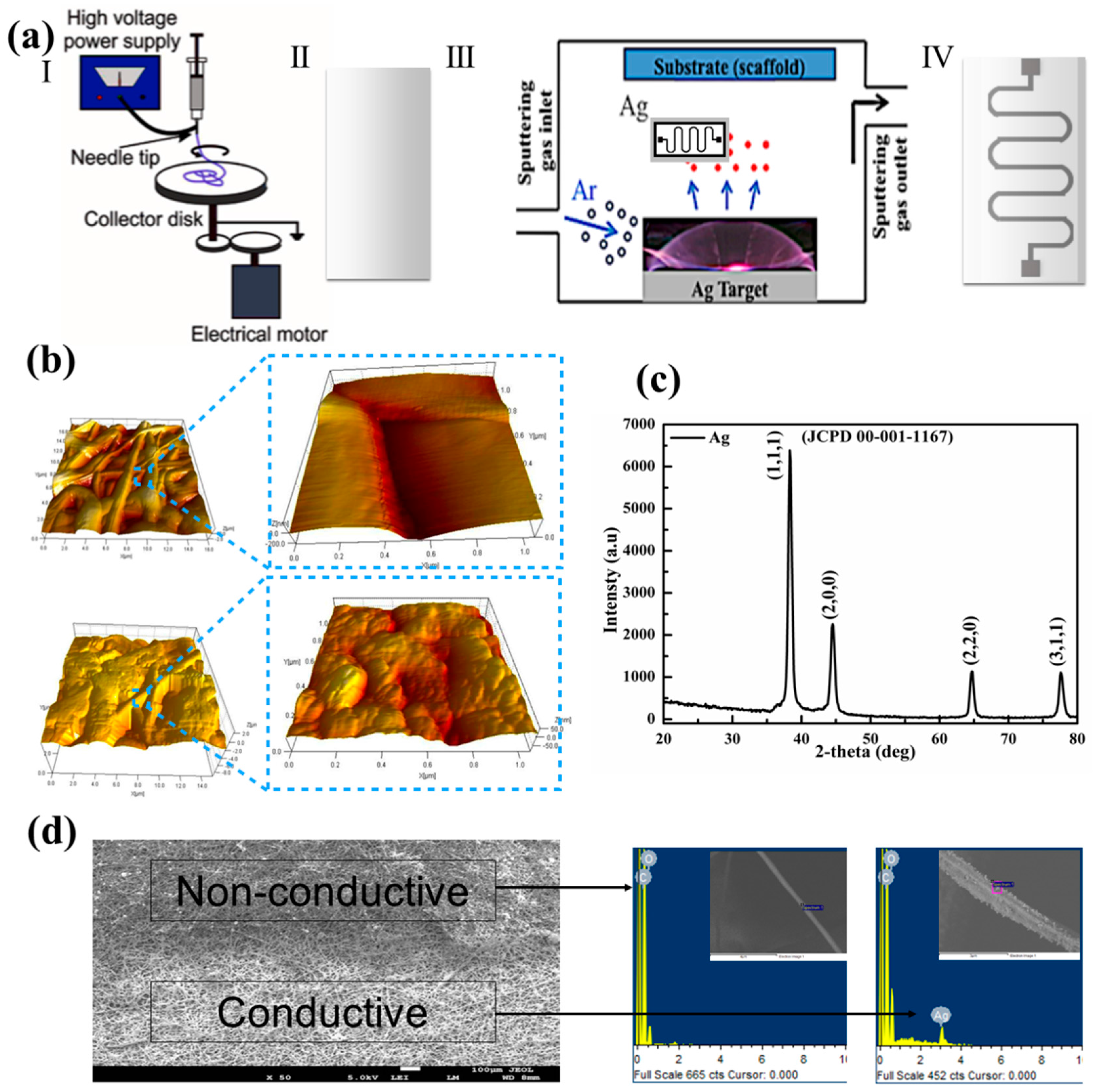
Abstract
:1. Introduction
2. Materials and Methods
2.1. Materials
2.2. Electrospinning
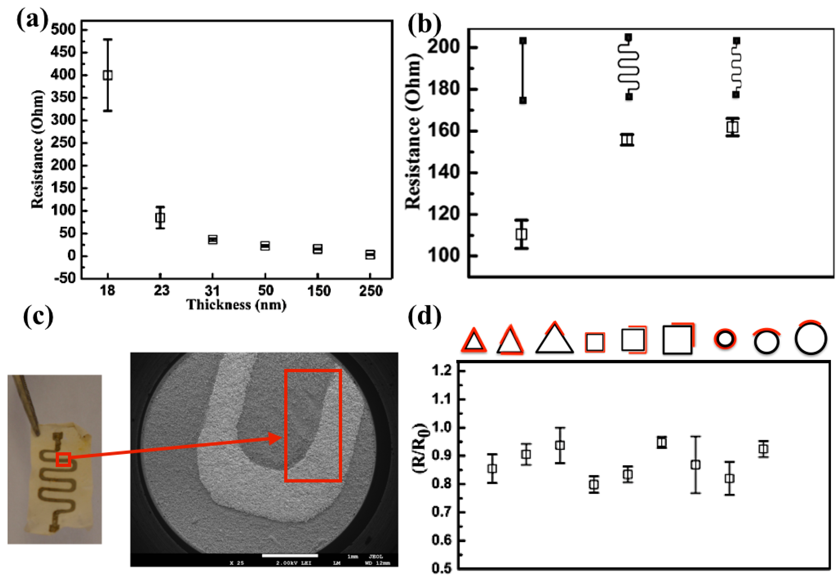
2.3. Fiber Coating Pattern
2.4. Morphological Characterizations
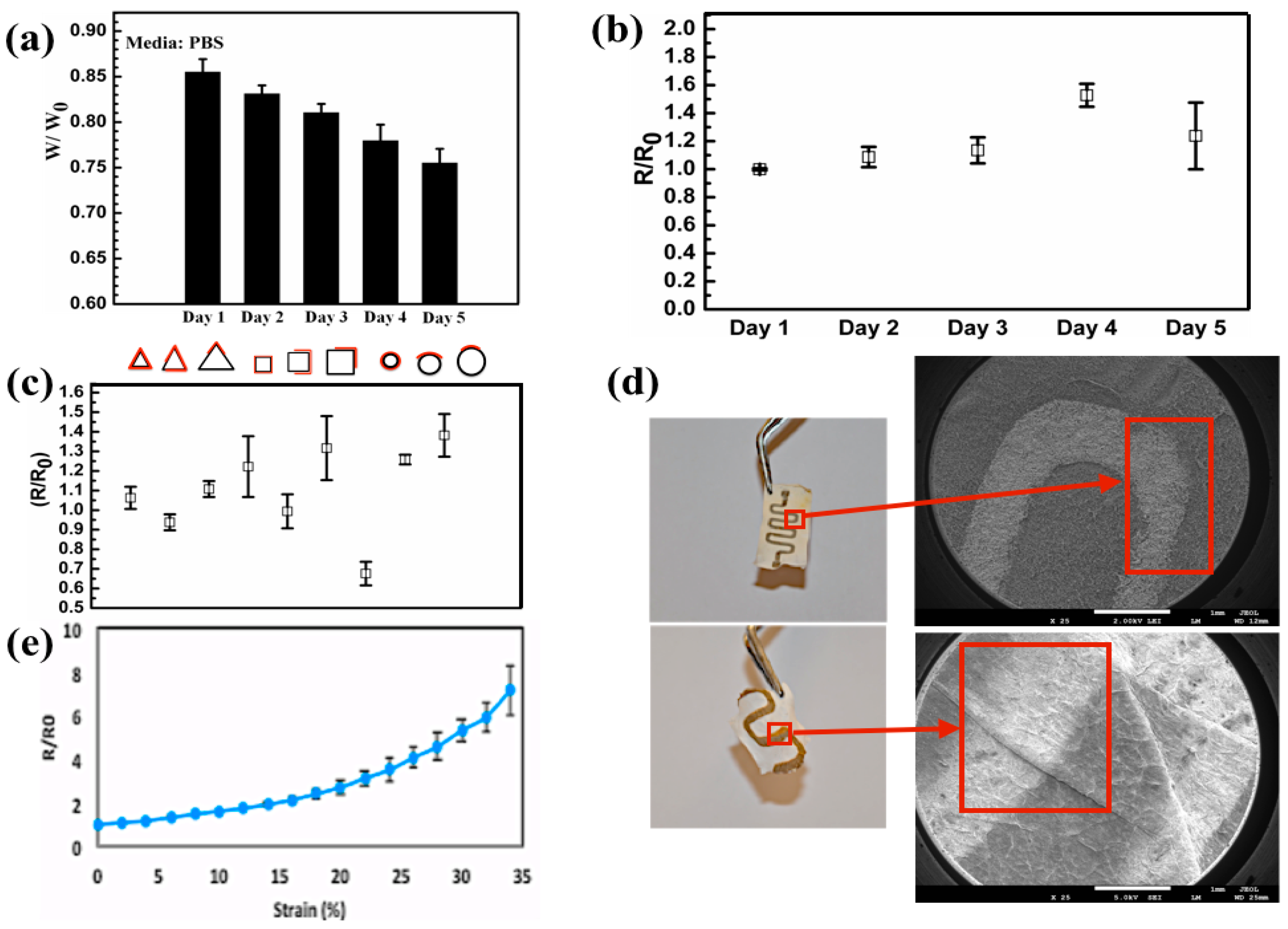
2.5. Mechanical Characterization
2.6. Degradation and Electrical Measurements
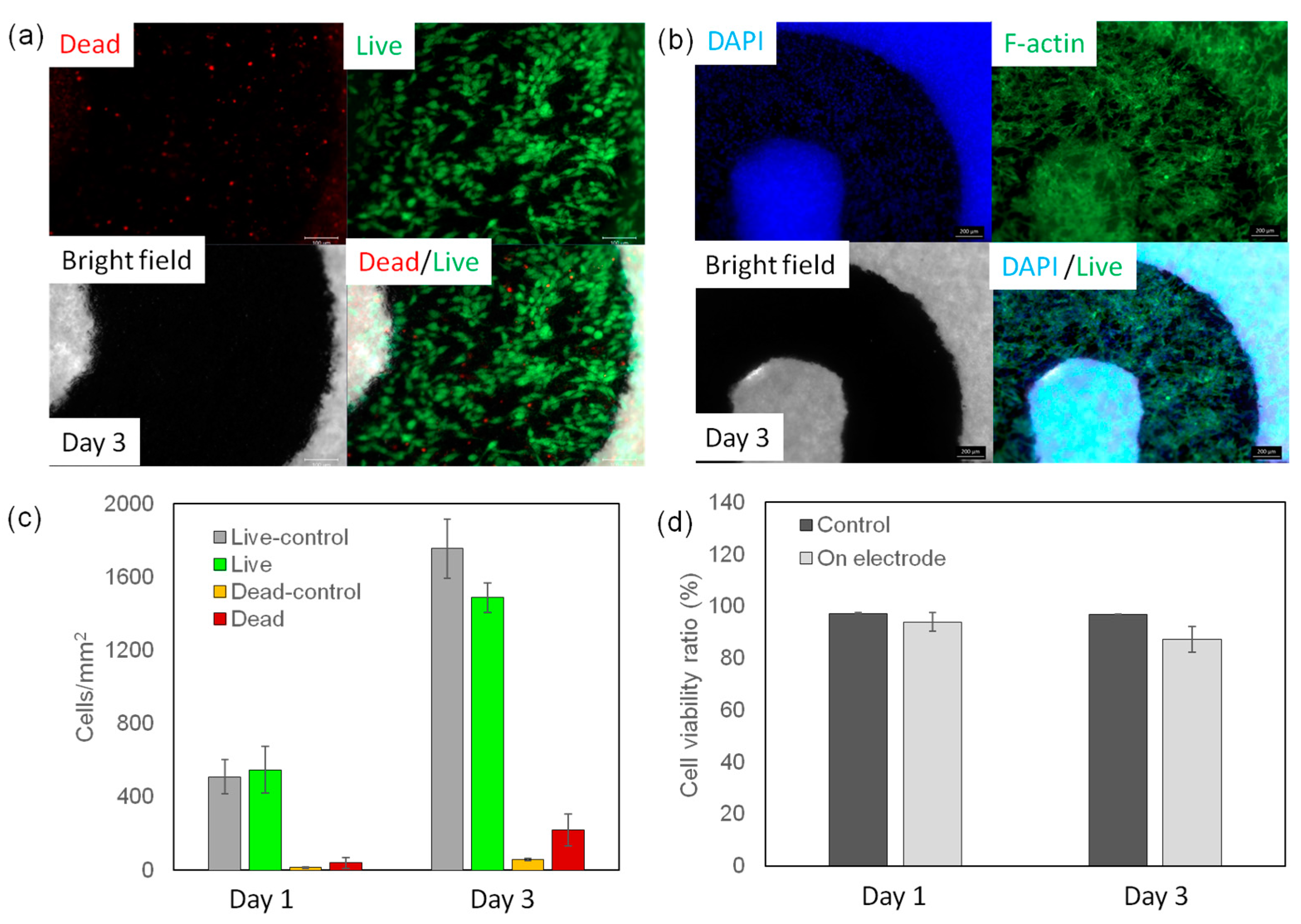
2.7. Cell Culture
3. Results and Discussion
4. Conclusions
Acknowledgments
Author Contributions
Conflicts of Interest
References
- Muskovich, M.; Bettinger, C.J. Biomaterials-based electronics: Polymers and interfaces for biology and medicine. Adv. Healthc. Mater. 2012, 1, 248–266. [Google Scholar] [CrossRef] [PubMed]
- Liao, C.; Zhang, M.; Yao, M.Y.; Hua, T.; Li, L.; Yan, F. Flexible organic electronics in biology: Materials and devices. Adv. Mater. 2015, 27, 7493–7527. [Google Scholar] [CrossRef] [PubMed]
- Nathan, A.; Ahnood, A.; Cole, M.T.; Lee, S.; Suzuki, Y.; Hiralal, P.; Bonaccorso, F.; Hasan, T.; Garcia-Gancedo, L.; Dyadyusha, A. Flexible electronics: The next ubiquitous platform. Proc. IEEE 2012, 100, 1486–1517. [Google Scholar] [CrossRef]
- Kim, D.H.; Wang, S.; Keum, H.; Ghaffari, R.; Kim, Y.S.; Tao, H.; Panilaitis, B.; Li, M.; Kang, Z.; Omenetto, F.; et al. Thin, flexible sensors and actuators as ’instrumented’ surgical sutures for targeted wound monitoring and therapy. Small 2012, 8, 3263–3268. [Google Scholar] [CrossRef] [PubMed]
- Irimia-Vladu, M.; Głowacki, E.D.; Voss, G.; Bauer, S.; Sariciftci, N.S. Green and biodegradable electronics. Mater. Today 2012, 15, 340–346. [Google Scholar] [CrossRef]
- Gardeniers, J.G.; van den Berg, A. Lab-on-a-chip systems for biomedical and environmental monitoring. Anal. Bioanal. Chem. 2004, 378, 1700–1703. [Google Scholar] [CrossRef] [PubMed]
- Delaney, J.L.; Hogan, C.F.; Tian, J.; Shen, W. Electrogenerated chemiluminescence detection in paper-based microfluidic sensors. Anal. Chem. 2011, 83, 1300–1306. [Google Scholar] [CrossRef] [PubMed]
- Tao, H.; Brenckle, M.A.; Yang, M.; Zhang, J.; Liu, M.; Siebert, S.M.; Averitt, R.D.; Mannoor, M.S.; McAlpine, M.C.; Rogers, J.A.; et al. Silk-based conformal, adhesive, edible food sensors. Adv. Mater. 2012, 24, 1067–1072. [Google Scholar] [CrossRef] [PubMed]
- Escarpa, A.; Gonzalez, M.C.; Crevillen, A.G.; Blasco, A.J. Ce microchips: An opened gate to food analysis. Electrophoresis 2007, 28, 1002–1011. [Google Scholar] [CrossRef] [PubMed]
- Ko, S.H.; Pan, H.; Grigoropoulos, C.P.; Luscombe, C.K.; Fréchet, J.M.; Poulikakos, D. All-inkjet-printed flexible electronics fabrication on a polymer substrate by low-temperature high-resolution selective laser sintering of metal nanoparticles. Nanotechnology 2007, 18, 345202. [Google Scholar] [CrossRef]
- Zschieschang, U.; Klauk, H.; Halik, M.; Schmid, G.; Dehm, C. Flexible organic circuits with printed gate electrodes. Adv. Mater. 2003, 15, 1147–1151. [Google Scholar] [CrossRef]
- Najafabadi, A.H.; Tamayol, A.; Annabi, N.; Ochoa, M.; Mostafalu, P.; Akbari, M.; Nikkhah, M.; Rahimi, R.; Dokmeci, M.R.; Sonkusale, S.; et al. Biodegradable nanofibrous polymeric substrates for generating elastic and flexible electronics. Adv. Mater. 2014, 26, 5823–5830. [Google Scholar] [CrossRef] [PubMed]
- Hwang, S.W.; Tao, H.; Kim, D.H.; Cheng, H.; Song, J.K.; Rill, E.; Brenckle, M.A.; Panilaitis, B.; Won, S.M.; Kim, Y.S.; et al. A physically transient form of silicon electronics. Science 2012, 337, 1640–1644. [Google Scholar] [CrossRef] [PubMed]
- Tao, H.; Chieffo, L.R.; Brenckle, M.A.; Siebert, S.M.; Liu, M.; Strikwerda, A.C.; Fan, K.; Kaplan, D.L.; Zhang, X.; Averitt, R.D. Metamaterials on paper as a sensing platform. Adv. Mater. 2011, 23, 3197–3201. [Google Scholar] [CrossRef] [PubMed]
- Sekitani, T.; Zschieschang, U.; Klauk, H.; Someya, T. Flexible organic transistors and circuits with extreme bending stability. Nat. Mater. 2010, 9, 1015–1022. [Google Scholar] [CrossRef] [PubMed]
- Bettinger, C.J.; Bao, Z. Organic thin-film transistors fabricated on resorbable biomaterial substrates. Adv. Mater. 2010, 22, 651–655. [Google Scholar] [CrossRef] [PubMed]
- Sen, C.K.; Gordillo, G.M.; Roy, S.; Kirsner, R.; Lambert, L.; Hunt, T.K.; Gottrup, F.; Gurtner, G.C.; Longaker, M.T. Human skin wounds: A major and snowballing threat to public health and the economy. Wound Repair Regen. 2009, 17, 763–771. [Google Scholar] [CrossRef] [PubMed]
- Zhang, Y.N.; Avery, R.K.; Vallmajo-Martin, Q.; Assmann, A.; Vegh, A.; Memic, A.; Olsen, B.D.; Annabi, N.; Khademhosseini, A. A Highly elastic and rapidly crosslinkable elastin-like polypeptide-based hydrogel for biomedical applications. Adv. Funct. Mater. 2015, 25, 4814–4826. [Google Scholar] [CrossRef] [PubMed]
- Shin, S.R.; Shin, C.; Memic, A.; Shadmehr, S.; Miscuglio, M.; Jung, H.Y.; Jung, S.M.; Bae, H.; Khademhosseini, A.; Tang, X.S. Aligned carbon nanotube–based flexible gel substrates for engineering biohybrid tissue actuators. Adv. Funct. Mater. 2015, 25, 4486–4495. [Google Scholar] [CrossRef] [PubMed]
- Association, A.B. Burn Incidence and Treatment in the United States: 2011 Fact Sheet; American Burn Association: Chicago, IL, USA, 2011. [Google Scholar]
- Lin, S.Y.; Chen, K.S.; Run-Chu, L. Design and evaluation of drug-loaded wound dressing having thermoresponsive, adhesive, absorptive and easy peeling properties. Biomaterials 2001, 22, 2999–3004. [Google Scholar] [CrossRef]
- Loke, W.K.; Lau, S.K.; Yong, L.L.; Khor, E.; Sum, C.K. Wound dressing with sustained anti-microbial capability. J. Biomed. Mater. Res. 2000, 53, 8–17. [Google Scholar] [CrossRef]
- Schneider, L.A.; Korber, A.; Grabbe, S.; Dissemond, J. Influence of pH on wound-healing: A new perspective for wound-therapy? Arch. Dermatol. Res. 2007, 298, 413–420. [Google Scholar] [CrossRef] [PubMed]
- Boateng, J.S.; Matthews, K.H.; Stevens, H.N.; Eccleston, G.M. Wound healing dressings and drug delivery systems: A review. J. Pharm. Sci. 2008, 97, 2892–2923. [Google Scholar] [CrossRef] [PubMed]
- Tamayol, A.; Akbari, M.; Annabi, N.; Paul, A.; Khademhosseini, A.; Juncker, D. Fiber-based tissue engineering: Progress, challenges, and opportunities. Biotechnol. Adv. 2013, 31, 669–687. [Google Scholar] [CrossRef] [PubMed]
- Annabi, N.; Tamayol, A.; Uquillas, J.A.; Akbari, M.; Bertassoni, L.E.; Cha, C.; Camci-Unal, G.; Dokmeci, M.R.; Peppas, N.A.; Khademhosseini, A. 25th anniversary article: Rational design and applications of hydrogels in regenerative medicine. Adv. Mater. 2014, 26, 85–123. [Google Scholar] [CrossRef] [PubMed]
- Greiner, A.; Wendorff, J.H. Electrospinning: A fascinating method for the preparation of ultrathin fibers. Angew. Chem. Int. Ed. Engl. 2007, 46, 5670–5703. [Google Scholar] [CrossRef] [PubMed]
- Ostrovidov, S.; Shi, X.; Zhang, L.; Liang, X.; Kim, S.B.; Fujie, T.; Ramalingam, M.; Chen, M.; Nakajima, K.; Al-Hazmi, F. Myotube formation on gelatin nanofibers–multi-walled carbon nanotubes hybrid scaffolds. Biomaterials 2014, 35, 6268–6277. [Google Scholar] [CrossRef] [PubMed]
- Hasan, A.; Memic, A.; Annabi, N.; Hossain, M.; Paul, A.; Dokmeci, M.R.; Dehghani, F.; Khademhosseini, A. Electrospun scaffolds for tissue engineering of vascular grafts. Acta Biomater. 2014, 10, 11–25. [Google Scholar] [CrossRef] [PubMed]
- Kenawy el, R.; Bowlin, G.L.; Mansfield, K.; Layman, J.; Simpson, D.G.; Sanders, E.H.; Wnek, G.E. Release of tetracycline hydrochloride from electrospun poly(ethylene-co-vinylacetate), poly(lactic acid), and a blend. J. Control. Release 2002, 81, 57–64. [Google Scholar] [CrossRef]
- Sant, S.; Hwang, C.M.; Lee, S.H.; Khademhosseini, A. Hybrid PGS-PCL microfibrous scaffolds with improved mechanical and biological properties. J. Tissue Eng. Regen. Med. 2011, 5, 283–291. [Google Scholar] [CrossRef] [PubMed]
- Wang, Y.; Ameer, G.A.; Sheppard, B.J.; Langer, R. A tough biodegradable elastomer. Nat. Biotechnol. 2002, 20, 602–606. [Google Scholar] [CrossRef] [PubMed]
- Jeong, J.W.; Yeo, W.H.; Akhtar, A.; Norton, J.J.; Kwack, Y.J.; Li, S.; Jung, S.Y.; Su, Y.; Lee, W.; Xia, J.; et al. Materials and optimized designs for human-machine interfaces via epidermal electronics. Adv. Mater. 2013, 25, 6839–6846. [Google Scholar] [CrossRef] [PubMed]
- Park, M.; Im, J.; Shin, M.; Min, Y.; Park, J.; Cho, H.; Park, S.; Shim, M.B.; Jeon, S.; Chung, D.Y.; et al. Highly stretchable electric circuits from a composite material of silver nanoparticles and elastomeric fibres. Nat. Nanotechnol. 2012, 7, 803–809. [Google Scholar] [CrossRef] [PubMed]
- Kim, Y.; Zhu, J.; Yeom, B.; Di Prima, M.; Su, X.; Kim, J.G.; Yoo, S.J.; Uher, C.; Kotov, N.A. Stretchable nanoparticle conductors with self-organized conductive pathways. Nature 2013, 500, 59–63. [Google Scholar] [CrossRef] [PubMed]
- Kim, Y.; Kim, H.; Yoo, H.-J. Electrical characterization of screen-printed circuits on the fabric. IEEE Trans. Adv. Packag. 2010, 33, 196–205. [Google Scholar]


© 2017 by the authors. Licensee MDPI, Basel, Switzerland. This article is an open access article distributed under the terms and conditions of the Creative Commons Attribution (CC BY) license ( http://creativecommons.org/licenses/by/4.0/).
Share and Cite
Memic, A.; Aldhahri, M.; Tamayol, A.; Mostafalu, P.; Abdel-wahab, M.S.; Samandari, M.; Moghaddam, K.M.; Annabi, N.; Bencherif, S.A.; Khademhosseini, A. Nanofibrous Silver-Coated Polymeric Scaffolds with Tunable Electrical Properties. Nanomaterials 2017, 7, 63. https://doi.org/10.3390/nano7030063
Memic A, Aldhahri M, Tamayol A, Mostafalu P, Abdel-wahab MS, Samandari M, Moghaddam KM, Annabi N, Bencherif SA, Khademhosseini A. Nanofibrous Silver-Coated Polymeric Scaffolds with Tunable Electrical Properties. Nanomaterials. 2017; 7(3):63. https://doi.org/10.3390/nano7030063
Chicago/Turabian StyleMemic, Adnan, Musab Aldhahri, Ali Tamayol, Pooria Mostafalu, Mohamed Shaaban Abdel-wahab, Mohamadmahdi Samandari, Kamyar Mollazadeh Moghaddam, Nasim Annabi, Sidi A. Bencherif, and Ali Khademhosseini. 2017. "Nanofibrous Silver-Coated Polymeric Scaffolds with Tunable Electrical Properties" Nanomaterials 7, no. 3: 63. https://doi.org/10.3390/nano7030063
APA StyleMemic, A., Aldhahri, M., Tamayol, A., Mostafalu, P., Abdel-wahab, M. S., Samandari, M., Moghaddam, K. M., Annabi, N., Bencherif, S. A., & Khademhosseini, A. (2017). Nanofibrous Silver-Coated Polymeric Scaffolds with Tunable Electrical Properties. Nanomaterials, 7(3), 63. https://doi.org/10.3390/nano7030063