N-Doped Graphene with Low Intrinsic Defect Densities via a Solid Source Doping Technique


Abstract

1. Introduction
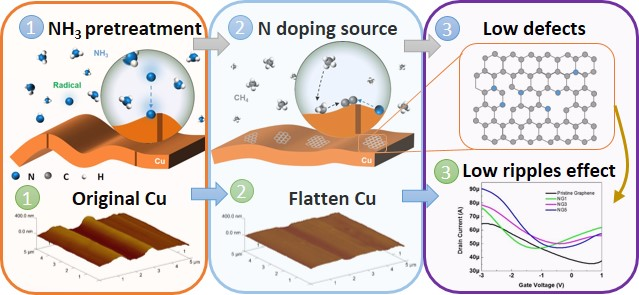
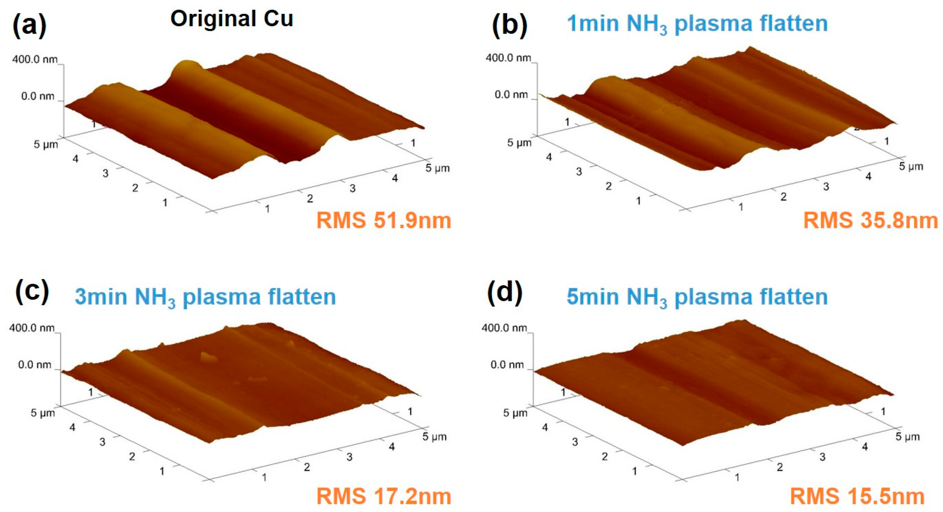
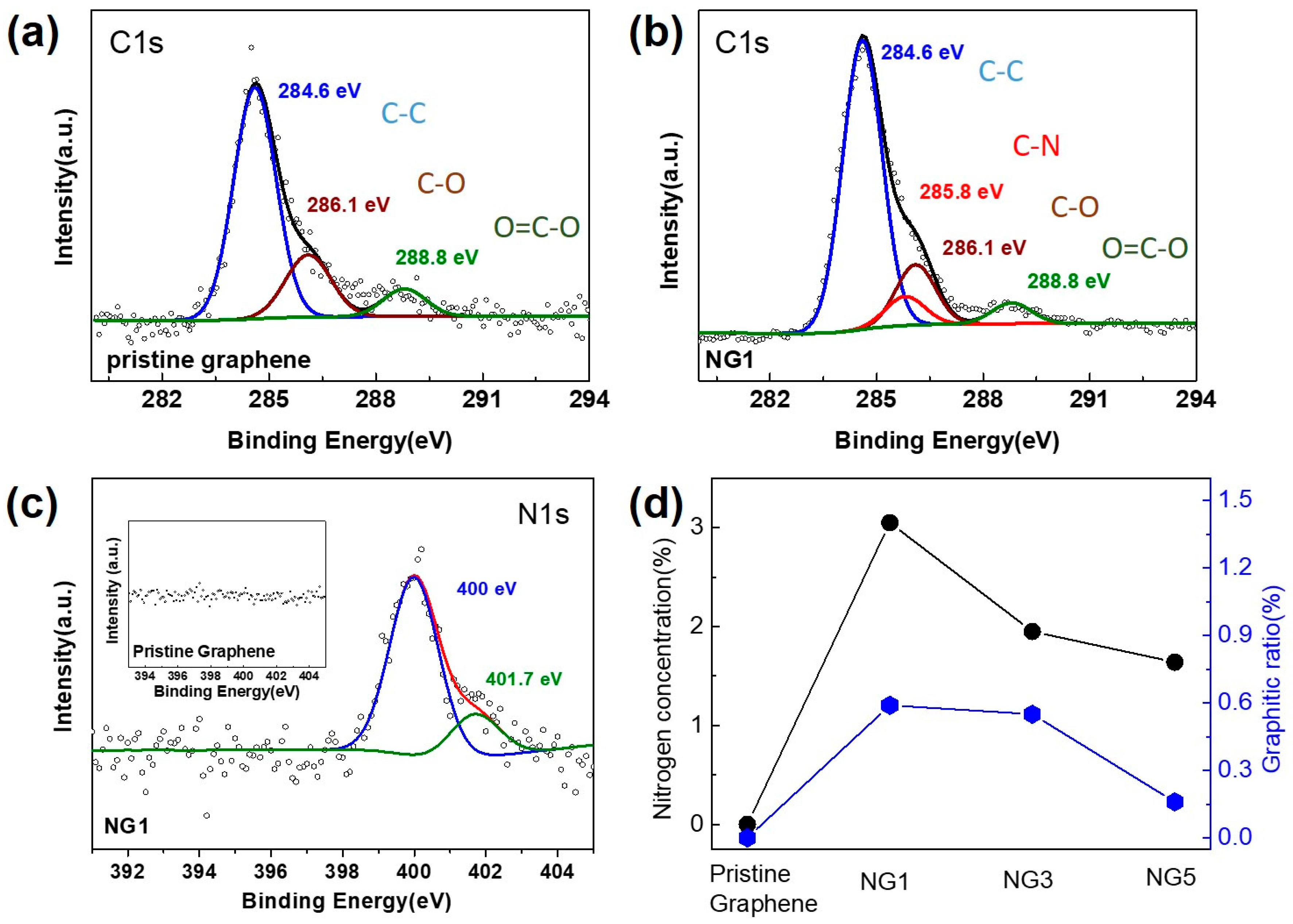
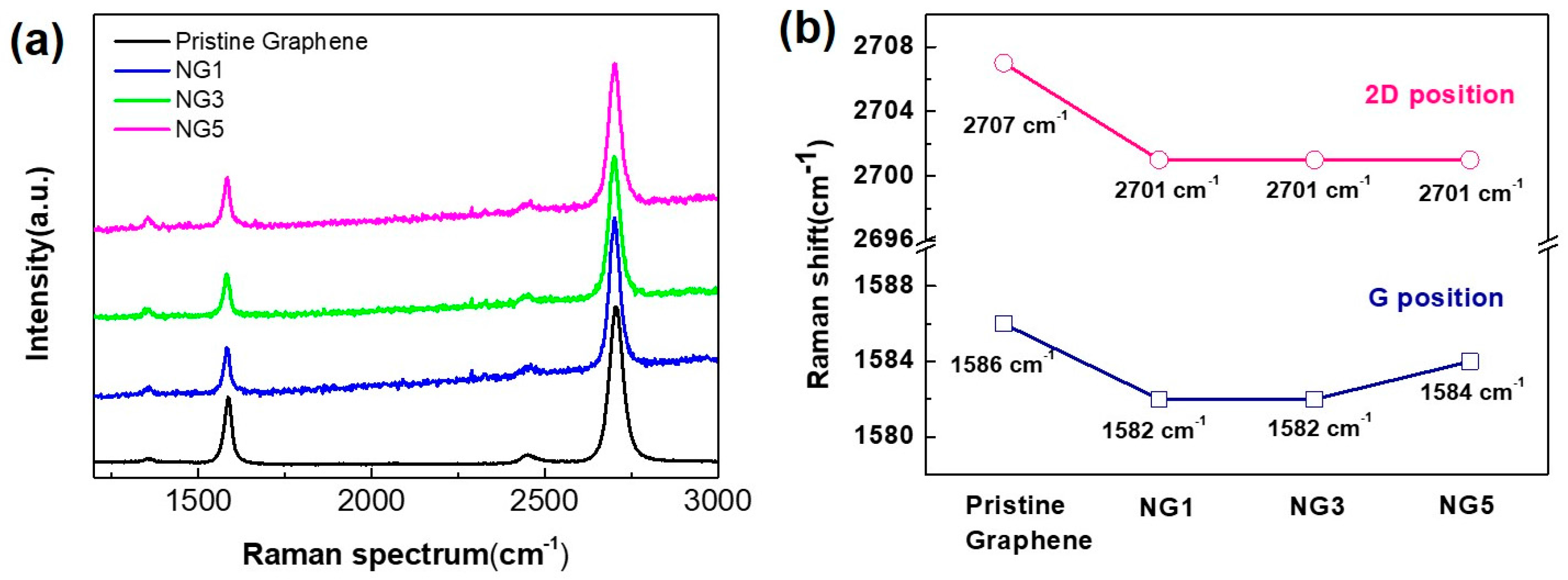
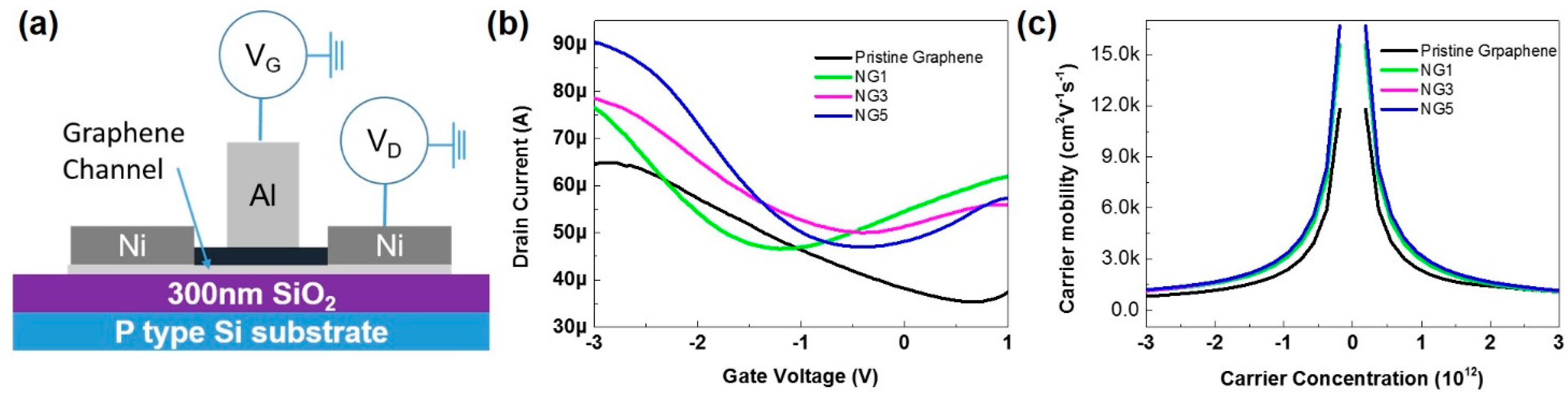
2. Results and Discussion
3. Conclusions
4. Methods
4.1. NH3 Plasma Pretreatment and AFM Scanning
4.2. Graphene Growth and Transfer Process
4.3. Raman Spectral Analysis and X-ray Photoelectron Spectroscopy
4.4. Top-Gated Graphene Field-Effect Transistors Fabrication and Measurement
Supplementary Materials
Acknowledgments
Author Contributions
Conflicts of Interest
References
- Agnoli, S.; Favaro, M. Doping graphene with boron: A review of synthesis. J. Mater. Chem. A Mater. Energy Sustain. 2016, 4, 5002–5025. [Google Scholar] [CrossRef]
- Guo, B.; Liu, Q.; Chen, E.; Zhu, H.; Fang, L.; Gong, J.R. Controllable N-doping of graphene. Nano Lett. 2010, 10, 4975–4980. [Google Scholar] [CrossRef] [PubMed]
- Ho, K.I.; Liao, J.H.; Huang, C.H.; Hsu, C.L.; Zhang, W.; Lu, A.Y.; Li, L.J.; Lai, C.S.; Su, C.Y. One-step formation of a single atomic-layer transistor by the selective fluorination of a graphene film. Small 2014, 10, 989–997. [Google Scholar] [CrossRef] [PubMed]
- Liang, C.; Wang, Y. Synthesis of sulfur-doped p-type graphene by annealing with hydrogen sulfide. Carbon 2014, 82, 506–512. [Google Scholar] [CrossRef]
- Choi, K.; Lee, S.; Shim, Y.; Oh, J.; Kim, S.; Park, S. Electrocatalytic performances of N-doped graphene with anchored iridium species in oxygen reduction reaction. 2D Mater. 2015, 2, 34019. [Google Scholar] [CrossRef]
- Chem, J.M.; Ma, C.; Cao, D. Nitrogen-doped graphene nanosheets as anode materials for lithium ion batteries: A first-principles study. J. Mater. Chem. 2012, 22, 8911–8915. [Google Scholar]
- Lv, R.; Li, Q.; Botello-Méndez, A.R.; Hayashi, T.; Wang, B.; Berkdemir, A.; Hao, Q.; Elías, A.L.; Cruz-Silva, R.; Gutiérrez, H.R.; et al. Nitrogen-doped graphene: Beyond single substitution and enhanced molecular sensing. Sci. Rep. 2012, 2, 586. [Google Scholar] [CrossRef] [PubMed]
- Jeong, H.M.; Lee, J.W.; Shin, W.H.; Choi, Y.J.; Shin, H.J.; Kang, J.K.; Choi, J.W. Nitrogen-Doped Graphene for High-Performance Ultracapacitors and the Importance of Nitrogen-Doped Sites at Basal Planes. Nano Lett. 2011, 11, 2472–2477. [Google Scholar] [CrossRef] [PubMed]
- Jin, Z.; Yao, J.; Kittrell, C.; Tour, J.M. Large-scale growth and characterizations of nitrogen-doped monolayer graphene sheets. ACS Nano 2011, 5, 4112–4117. [Google Scholar] [CrossRef] [PubMed]
- Meyer, J.C.; Kurasch, S.; Park, H.J.; Skakalova, V.; Künzel, D.; Gross, A.; Chuvilin, A.; Algara-siller, G.; Roth, S.; Iwasaki, T.; et al. Experimental anaysis of charge redistribution due to chemical bonding by high resolution transmission electron microscopy. Nat. Mater. 2011, 10, 209–215. [Google Scholar] [CrossRef] [PubMed]
- Boutchich, M.; Arezki, H.; Alamarguy, D.; Ho, K.-I.; Sediri, H.; Güneş, F.; Alvarez, J.; Kleider, J.P.; Lai, C.S.; Ouerghi, A. Atmospheric pressure route to epitaxial nitrogen-doped trilayer graphene on 4H-SiC (0001) substrate. Appl. Phys. Lett. 2014, 105, 233111. [Google Scholar] [CrossRef]
- Lin, L.; Liao, L.; Yin, J.; Peng, H.; Liu, Z. Building graphene p–n junctions for next-generation photodetection. Nano Today 2015, 10, 701–716. [Google Scholar] [CrossRef]
- Jariwala, D.; Marks, T.J.; Hersam, M.C. Mixed-dimensional van der Waals heterostructures. Nat. Mater. 2017, 16, 170–181. [Google Scholar] [CrossRef] [PubMed]
- Wang, H.; Maiyalagan, T.; Wang, X. Review on Recent Progress in Nitrogen-Doped Graphene: Synthesis, Characterization, and Its Potential Applications. ACS Catal. 2012, 2, 781–794. [Google Scholar] [CrossRef]
- Li, X.; Wang, H.; Robinson, J.T.; Sanchez, H.; Diankov, G. Simultaneous Nitrogen Doping and Reduction of Graphene Oxide. J. Am. Chem. Soc. 2009, 131, 15939–15944. [Google Scholar] [CrossRef] [PubMed]
- Lin, Y.; Ksari, Y.; Aubel, D.; Hajjar-garreau, S.; Spiegel, Y.; Roux, L.; Simon, L.; Themlin, J. Efficient and low-damage nitrogen doping of graphene via plasmabased methods. Carbon 2016, 100, 337–344. [Google Scholar] [CrossRef]
- Wei, D.; Peng, L.; Li, M.; Mao, H.; Niu, T.; Han, C.; Chen, W.; Wee, A.T.S. Low Temperature Critical Growth of High Quality Nitrogen Doped Graphene on Dielectrics by Plasma-Enhanced Chemical Vapor Deposition. ACS Nano 2015, 9, 164–171. [Google Scholar] [CrossRef] [PubMed]
- Imamura, G.; Saiki, K. Effect of UV light-induced nitrogen doping on the field effect transistor characteristics of graphene. RSC Adv. 2015, 5, 70522–70526. [Google Scholar] [CrossRef]
- Sui, Y.; Zhu, B.; Zhang, H.; Shu, H.; Chen, Z.; Zhang, Y.; Zhang, Y.; Wang, B.; Tang, C.; Xie, X.; et al. Temperature-dependent nitrogen configuration of N-doped graphene by chemical vapor deposition. Carbon 2014, 81, 814–820. [Google Scholar] [CrossRef]
- Lu, Y.-F.; Lo, S.-T.; Lin, J.-C.; Zhang, W.; Lu, J.-Y.; Liu, F.-H.; Tseng, C.-M.; Lee, Y.-H.; Liang, C.-T.; Li, L.-J. Nitrogen-Doped Graphene Sheets Grown by Chemical Vapor Deposition: Synthesis and Influence of Nitrogen Impurities on Carrier Transport. ACS Nano 2013, 7, 6522–6532. [Google Scholar] [CrossRef] [PubMed]
- Fasolino, A.; Katsnelson, M.I. Intrinsic ripples in graphene. Nat. Mater. 2007, 6, 6–9. [Google Scholar] [CrossRef] [PubMed]
- Cress, C.D.; Schmucker, S.W.; Friedman, A.L.; Dev, P.; Culbertson, J.C.; Lyding, J.W.; Robinson, J.T. Nitrogen doped graphene and twisted bilayer graphene via hyperthermal ion implantation with depth control. ACS Nano 2016, 10, 3714–3722. [Google Scholar] [CrossRef] [PubMed]
- Christiansen, S.; Fau, E.; Staudtstrasse, B. Efficient Nitrogen Doping of Single-Layer Graphene Accompanied by Negligible Defect Generation for Integration into Hybrid Semiconductor Heterostructures. ACS Appl. Mater. 2017, 9, 10003–10011. [Google Scholar]
- Liu, B.; Chiu, I.; Lai, C. Improvements on thermal stability of graphene and top gate graphene transistors by Ar annealing. Vaccum 2017, 137, 8–13. [Google Scholar] [CrossRef]
- Zhang, S.; Tsuzuki, S.; Ueno, K.; Dokko, K.; Watanabe, M. Upper Limit of Nitrogen Content in Carbon Materials. Angew. Chem. Int. Ed. 2015, 54, 1302–1306. [Google Scholar] [CrossRef] [PubMed]
- Moselund, K.E.; Ghoneim, H.; Schmid, H.; Bj, M.T. Solid-state diffusion as an efficient doping method for silicon nanowires and nanowire field effect transistors. Nanotechnology 2010, 21, 435202. [Google Scholar] [CrossRef] [PubMed]
- Resasco, J.; Dasgupta, N.P.; Rosell, J.R.; Guo, J.; Yang, P. Uniform Doping of Metal Oxide Nanowires Using Solid State. J. Am. Chem. Soc. 2014, 136, 10521–10526. [Google Scholar] [CrossRef] [PubMed]
- Kang, K.; Watanabe, S.; Broch, K.; Sepe, A.; Brown, A.; Nasrallah, I.; Nikolka, M.; Fei, Z.; Heeney, M.; Matsumoto, D.; et al. Sirringhaus, 2D coherent charge transport in highly ordered conducting polymers doped by solid state diffusion. Nat. Mater. 2016, 15, 896. [Google Scholar] [CrossRef] [PubMed]
- Zhang, C.; Fu, L.; Liu, N.; Liu, M.; Wang, Y.; Liu, Z. Synthesis of nitrogen-doped graphene using embedded carbon and nitrogen sources. Adv. Mater. 2011, 23, 1020–1024. [Google Scholar] [CrossRef] [PubMed]
- Noguchi, J.; Ohashi, N.; Jimbo, T.; Yamaguchi, H.; Takeda, K.; Hinode, K. Effect of NH3-Plasma Treatment and CMP Modification on TDDB Improvement in Cu. IEEE Trans. Electron Devices 2001, 48, 1340–1345. [Google Scholar] [CrossRef]
- Chang, Y.; Leu, J.; Lin, B.; Wang, Y.; Cheng, Y. Comparison of H2 and NH3 Treatments for Copper Interconnects. Adv. Mater. Sci. Eng. 2013, 2013, 825195. [Google Scholar] [CrossRef]
- Junhwan, O.; Lee, S.; Kim, J.; Lee, C. Effects of Plasma Cleaning of the Cu Seed Layer Surface on Cu Electroplating. J. Korean Phys. Soc. 2001, 39, 472–477. [Google Scholar]
- Vairagar, A.V.; Gan, Z.; Shao, W.; Mhaisalkar, S.G.; Li, H.; Tu, K.N.; Chen, Z.; Zschech, E.; Engelmann, H.J.; Zhang, S. Improvement of Electromigration Lifetime of Submicrometer Dual-Damascene Cu Interconnects Through Surface Engineering. J. Electrochem. Soc. 2006, 153, 840–845. [Google Scholar] [CrossRef]
- Lee, D.; Kwon, G.D.; Kim, J.H.; Moyen, E.; Lee, Y.H.; Baik, S.; Pribat, D. Significant enhancement of the electrical transport properties of graphene films by controlling the surface roughness of Cu foils before and during chemical vapor deposition. Nanoscale 2014, 6, 12943–12951. [Google Scholar] [CrossRef] [PubMed]
- Wei, D.; Liu, Y.; Wang, Y.; Zhang, H.; Huang, L.; Yu, G. Synthesis of n-doped graphene by chemical vapor deposition and its electrical properties. Nano Lett. 2009, 9, 1752–1758. [Google Scholar] [CrossRef] [PubMed]
- Wang, C.; Schouteden, K.; Wu, Q.; Li, Z. Atomic resolution of nitrogen-doped graphene on Cu foils. Nanotechnology 2016, 27, 1–9. [Google Scholar] [CrossRef] [PubMed]
- Xu, W.; Lim, T.S.; Seo, H.K.; Min, S.Y.; Cho, H.; Park, M.H.; Kim, Y.H.; Lee, T.W. N-doped graphene field-effect transistors with enhanced electron mobility and air-stability. Small 2014, 10, 1999–2005. [Google Scholar] [CrossRef] [PubMed]
- Ferrari, A.C.; Basko, D.M. Raman spectroscopy as a versatile tool for studying the properties of graphene. Nat. Nanotechnol. 2013, 8, 235–246. [Google Scholar] [CrossRef] [PubMed]
- Leong, W.S.; Gong, H.; Thong, J.T.L. Low-Contact-Resistance Graphene Devices with Nickel-Etch. ACS Nano 2014, 8, 994–1001. [Google Scholar] [CrossRef] [PubMed]
- Giubileo, F.; Di, A. Progress in Surface Science The role of contact resistance in graphene field-effect devices. Prog. Surf. Sci. 2017, 92, 143–175. [Google Scholar] [CrossRef]
- Bartolomeo, A.D.; Santandrea, S.; Giubileo, F.; Romeo, F.; Petrosino, M.; Citro, R.; Barbara, P.; Lupina, G.; Schroeder, T.; Rubino, A. Effect of back-gate on contact resistance and on channel conductance in graphene-based field-effect transistors. Diam. Relat. Mater. 2013, 38, 19–23. [Google Scholar] [CrossRef]
- Lee, K.H.; Shin, H.; Lee, J.; Lee, I.; Kim, G.; Choi, J.; Kim, S. Large-Scale Synthesis of High-Quality Hexagonal Boron Nitride Nanosheets for Large-Area Graphene Electronics. Nano Lett. 2012, 12, 714–718. [Google Scholar] [CrossRef] [PubMed]
- Novikov, D.S. Numbers of donors and acceptors from transport measurements in graphene. Appl. Phys. Lett. 2009, 91, 666. [Google Scholar] [CrossRef]
- Ho, K.I.; Boutchich, M.; Su, C.Y.; Moreddu, R.; Sebastian, E.S.; Marianathan, R.; Montes, L.; Lai, C.S. A Self-Aligned High-Mobility Graphene Transistor: Decoupling the Channel with Fluorographene to Reduce Scattering. Adv. Mater. 2015, 27, 6519. [Google Scholar] [CrossRef] [PubMed]
- Chen, J.; Cullen, W.G.; Jang, C.; Fuhrer, M.S.; Williams, E.D. Defect Scattering in Graphene. Phys. Rev. Lett. 2009, 102, 236805. [Google Scholar] [CrossRef] [PubMed]
- He, B.; Ren, Z.; Qi, C.; Yan, S.; Wang, Z. Synthesis of nitrogen-doped monolayer graphene with high transparent and n-type electrical properties. J. Mater. Chem. C 2015, 3, 6172–6177. [Google Scholar] [CrossRef]
- Luo, Z.; Lim, S.; Tian, Z.; Shang, J.; Lai, L.; MacDonald, B.; Fu, C.; Shen, Z.; Yu, T.; Lin, J. Pyridinic N doped graphene: Synthesis, electronic structure, and electrocatalytic property. J. Mater. Chem. 2011, 21, 8038–8044. [Google Scholar] [CrossRef]
- Li, J.; Ren, Z.; Zhou, Y.; Wu, X.; Xu, X.; Li, W.; Bai, J.; Wang, L.; Qi, M. Scalable synthesis of pyrrolic N-doped graphene by atmospheric pressure chemical vapor deposition and its terahertz response. Carbon 2013, 62, 330–336. [Google Scholar] [CrossRef]
- Qu, L.; Liu, Y.; Baek, J.B.; Dai, L. Nitrogen-doped graphene as efficient metal-free electrocatalyst for oxygen reduction in fuel cells. ACS Nano 2010, 4, 1321–1326. [Google Scholar] [CrossRef] [PubMed]
- Ho, K.-I.; Huang, C.-H.; Liao, J.-H.; Zhang, W.; Li, L.-J.; Lai, C.-S.; Su, C.-Y. Fluorinated Graphene as High Performance Dielectric Materials and the Applications for Graphene Nanoelectronics. Sci. Rep. 2014, 4, 5893. [Google Scholar] [CrossRef] [PubMed]
- Lu, C.-C.; Lin, Y.-C.; Yeh, C.-H.; Huang, J.-C.; Chiu, P.-W. High Mobility Flexible Graphene Field-Effect Transistors with Self-Healing Gate Dielectrics. ACS Nano 2012, 6, 4469–4474. [Google Scholar] [CrossRef] [PubMed]


| N-Doped Graphene Synthesis Method | Synthesis Temperature | Nitrogen Content (*) | Nitrogen Configurations (#) | ID/IG | Dirac Point Shift | Carrier mobility N-Doped Graphene/Pristine Graphene (cm2·V−1·s−1) | Ref. |
|---|---|---|---|---|---|---|---|
| CVD monolayer graphene growth on NH3 plasma pre-treated Cu foil | 1000 °C | 3% | Pyrrolic, Graphitic | 0.17 | 0.7 to −1.2 V (top gate) | ~1100/~1000 (electron branch) ~1100/800 (hole branch) | This work |
| CVD monolayer graphene growth on Cu using C2H2, H2 and NH3 as precursors | 900 °C | 16% | Pyridinic | >2 | N/A | N/A | [47] |
| CVD monolayer graphene growth on Cu using CH4 and NH3 as precursors | 1000 °C | 6.4% | Pyrrolic | ~0.7 | N/A | N/A | [48] |
| CVD monolayer graphene growth on Cu (CH4 + NH3) | 800 °C | 8.9% | Graphitic | ~0.30 | N/A | 450/1200 | [35] |
| CVD few-layered (2–8 layers) graphene growth on Ni (CH4 + NH3 + Ar) | 1000 °C | 4% | Pyrrolic, Pyridinic | 0.06–0.25 | N/A | N/A | [49] |
| CVD few-layered graphene growth on Ni with embedded nitrogen | 1000 °C | 2.9% | Pyrrolic, Pyridinic, Graphitic | 2.1 | more than 60 to −50 V (back gate) | N/A | [29] |
| CVD on Cu using pyridine as the precursor | 1000 °C | 2.4% | Pyridinic, Pyrrolic | 0.3–0.4 | 10 to −10 V (back gate) | 5/2000 | [9] |
| PECVD growth of NG on SiO2/Si using C2H2 and NH3 plasma as precursors | 475 °C | N/A | Pyridinic | ~0.7 | 20 to −20 V (back gate) | 400/NA | [17] |
| Post-annealing of CVD graphene (on Cu foil) in NH3 gas | 850 °C | 0.25% | Pyrrolic, Pyridinic | ~1 | N/A | N/A | [7] |
| Exfoliated graphene with N2 ion implantation and post-annealing in NH3 | 1100 °C | 1.1% | Pyridinic | ~0.6 | ~2 V to ~−7 V (back gate) | 6000/6700 (electron branch) 6000/15000 (hole branch) | [2] |
© 2017 by the authors. Licensee MDPI, Basel, Switzerland. This article is an open access article distributed under the terms and conditions of the Creative Commons Attribution (CC BY) license (http://creativecommons.org/licenses/by/4.0/).
Share and Cite
Liu, B.; Yang, C.-M.; Liu, Z.; Lai, C.-S. N-Doped Graphene with Low Intrinsic Defect Densities via a Solid Source Doping Technique. Nanomaterials 2017, 7, 302. https://doi.org/10.3390/nano7100302
Liu B, Yang C-M, Liu Z, Lai C-S. N-Doped Graphene with Low Intrinsic Defect Densities via a Solid Source Doping Technique. Nanomaterials. 2017; 7(10):302. https://doi.org/10.3390/nano7100302
Chicago/Turabian StyleLiu, Bo, Chia-Ming Yang, Zhiwei Liu, and Chao-Sung Lai. 2017. "N-Doped Graphene with Low Intrinsic Defect Densities via a Solid Source Doping Technique" Nanomaterials 7, no. 10: 302. https://doi.org/10.3390/nano7100302
APA StyleLiu, B., Yang, C.-M., Liu, Z., & Lai, C.-S. (2017). N-Doped Graphene with Low Intrinsic Defect Densities via a Solid Source Doping Technique. Nanomaterials, 7(10), 302. https://doi.org/10.3390/nano7100302