
Enhanced End-Contacts by Helium Ion Bombardment to Improve Graphene-Metal Contacts


Abstract
:
1. Introduction
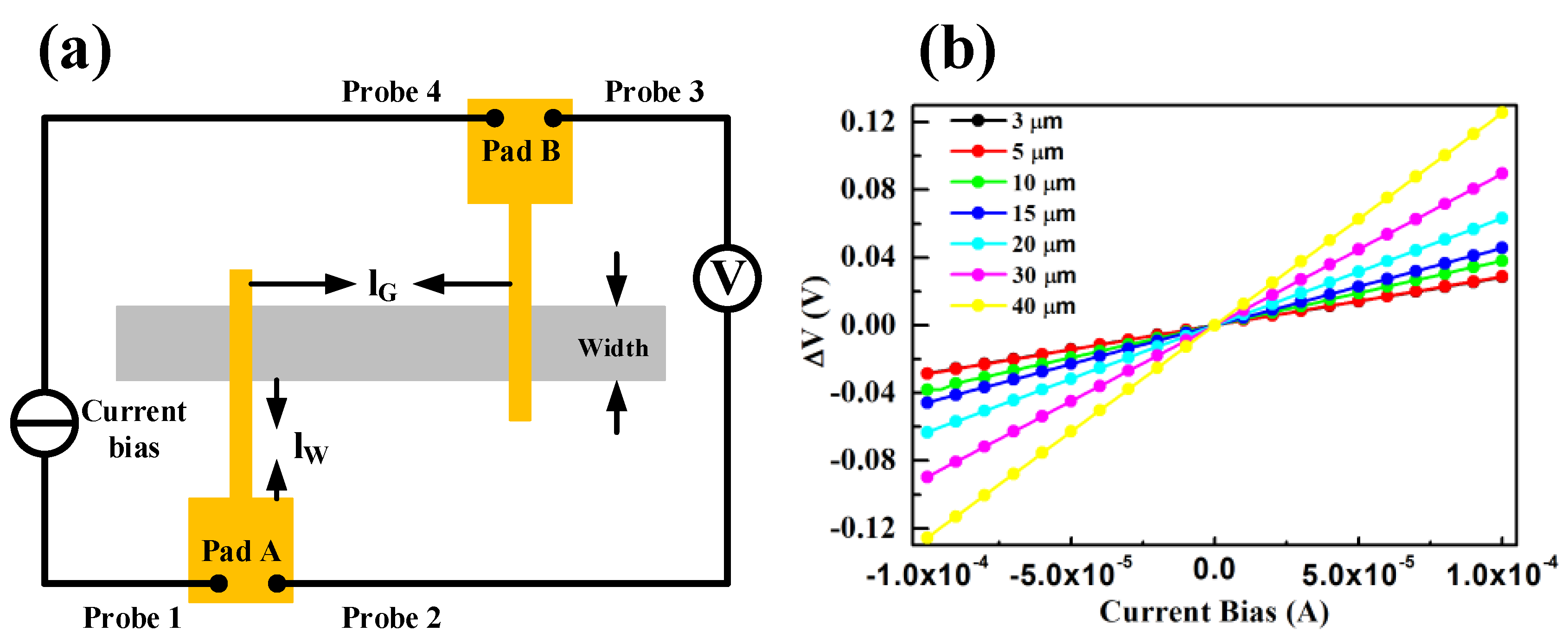
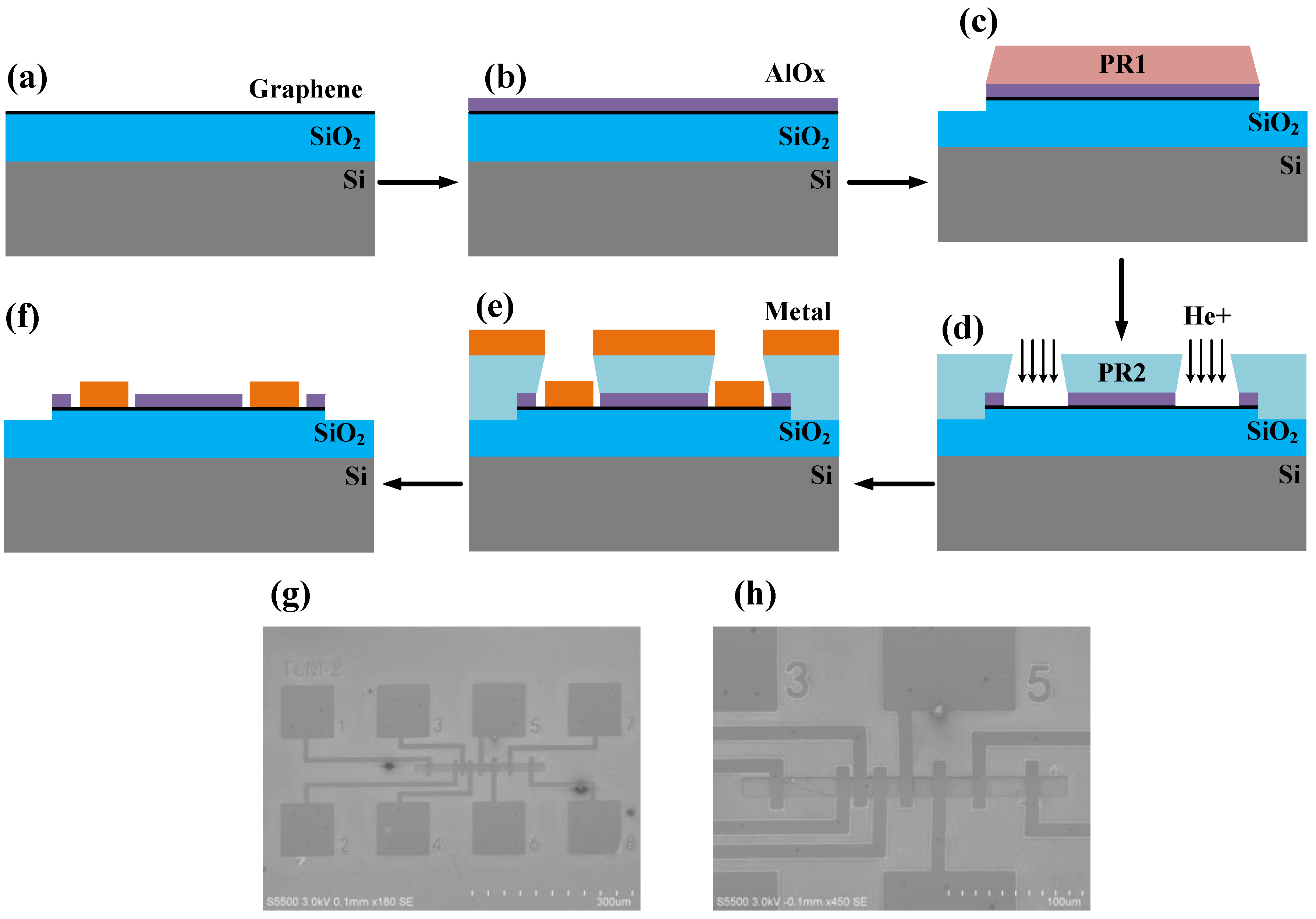
2. Experiment
3. Results
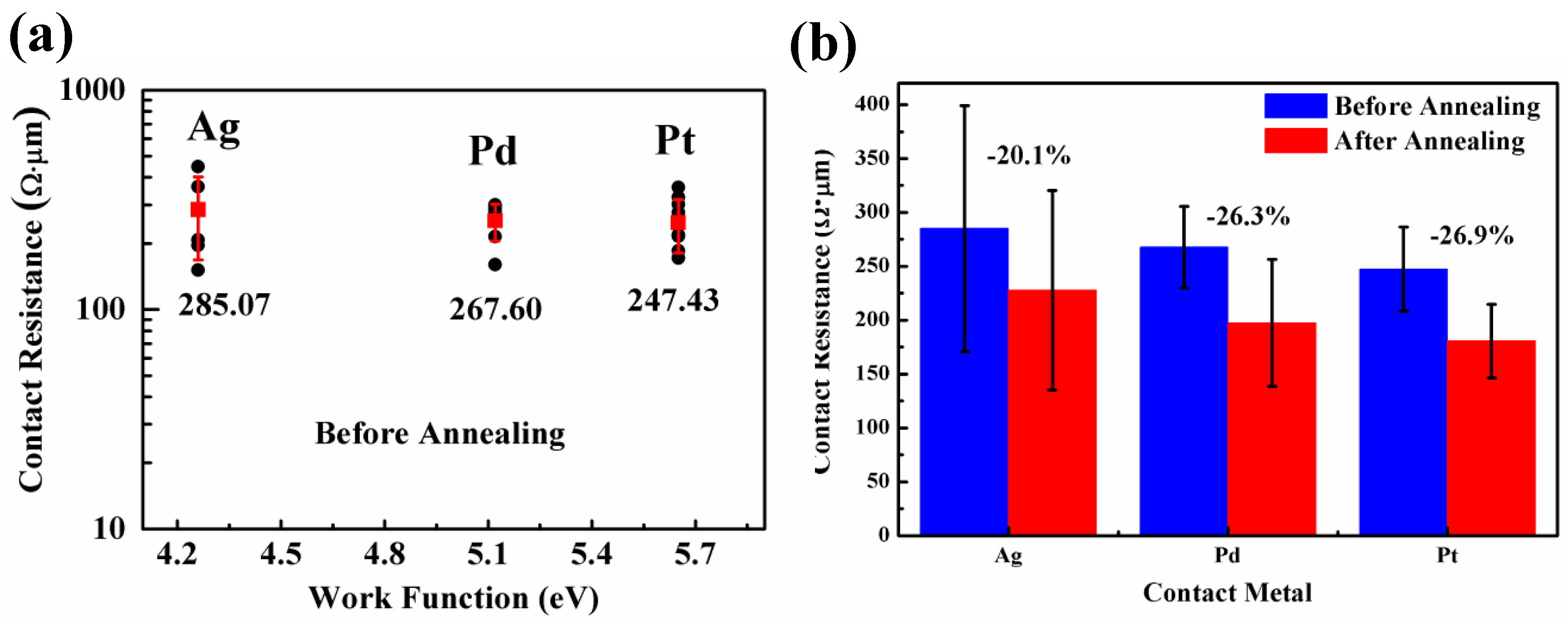
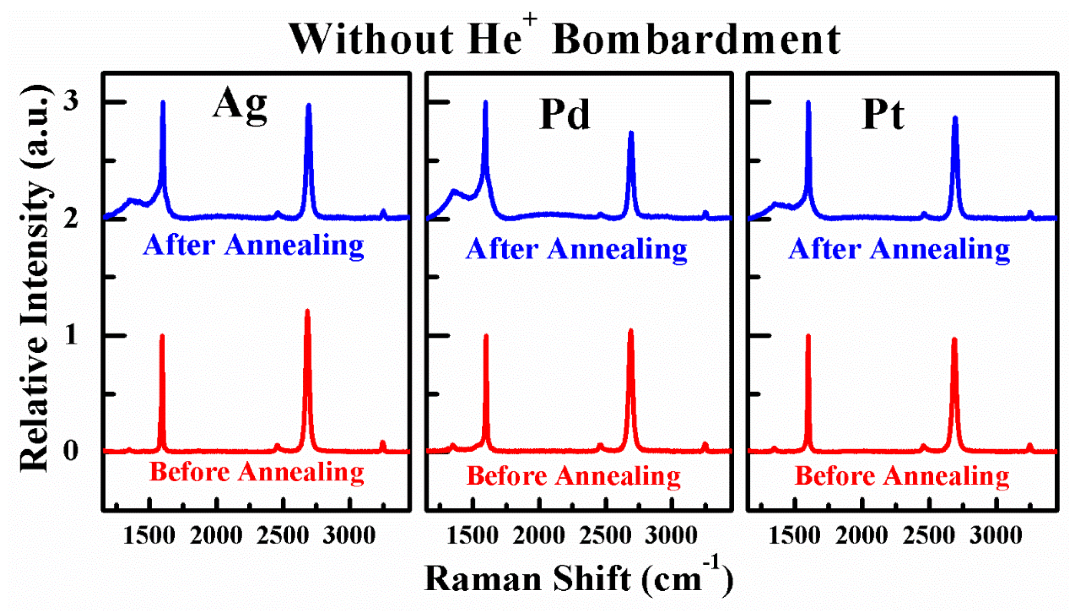
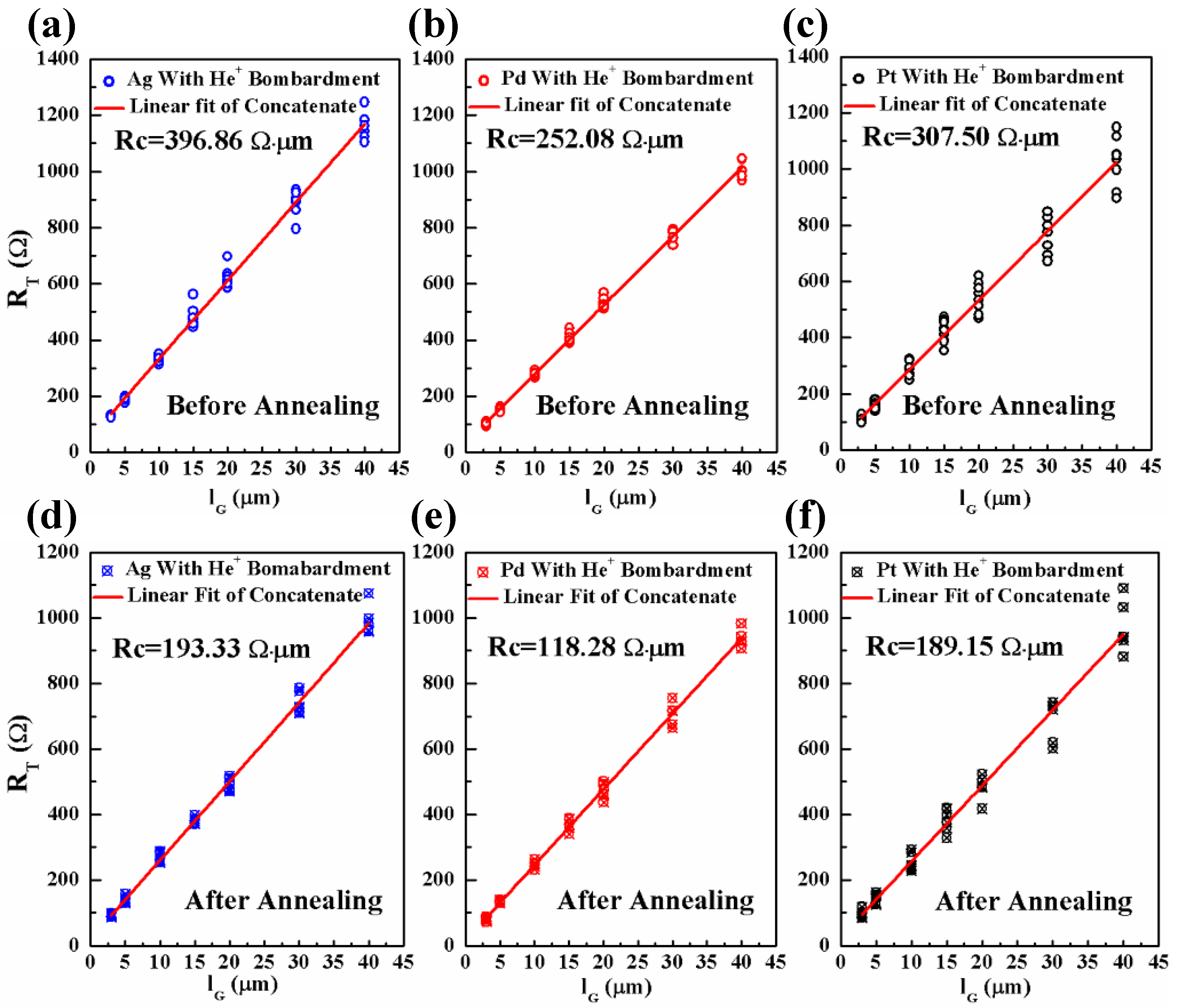
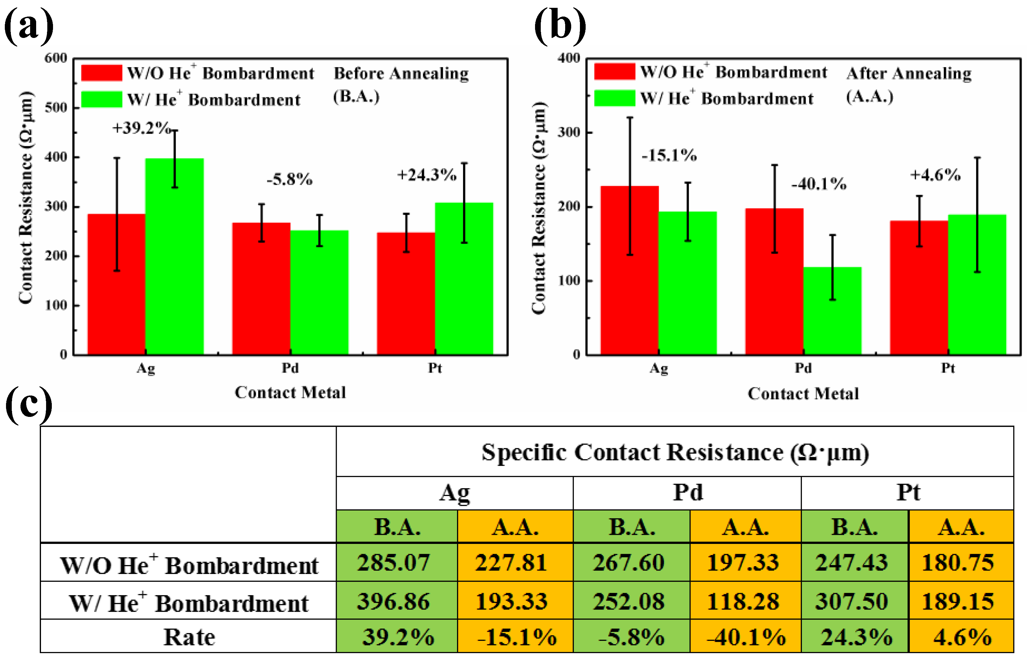
3.1. Effect of Annealing on the G-M Contact Properties
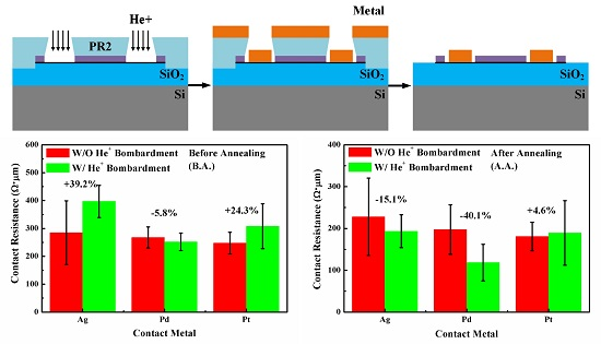
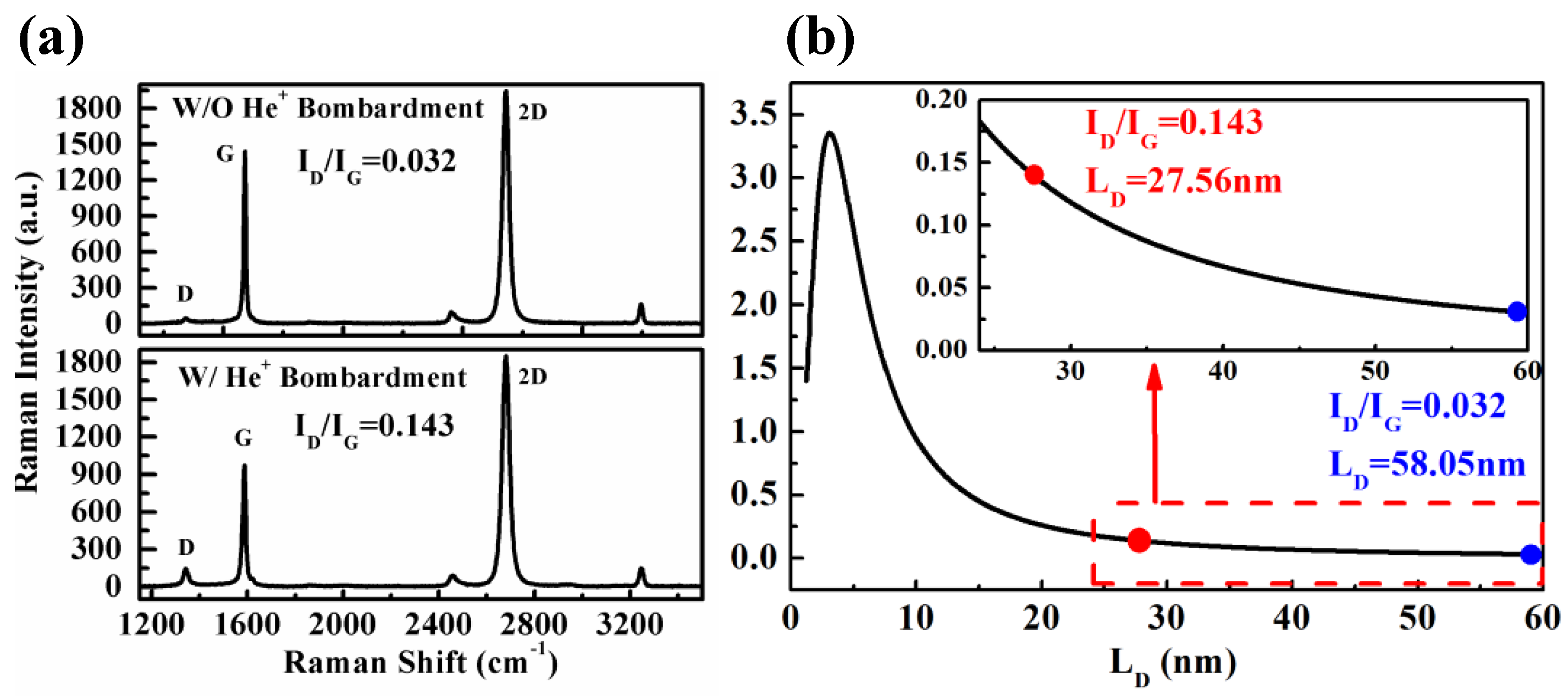
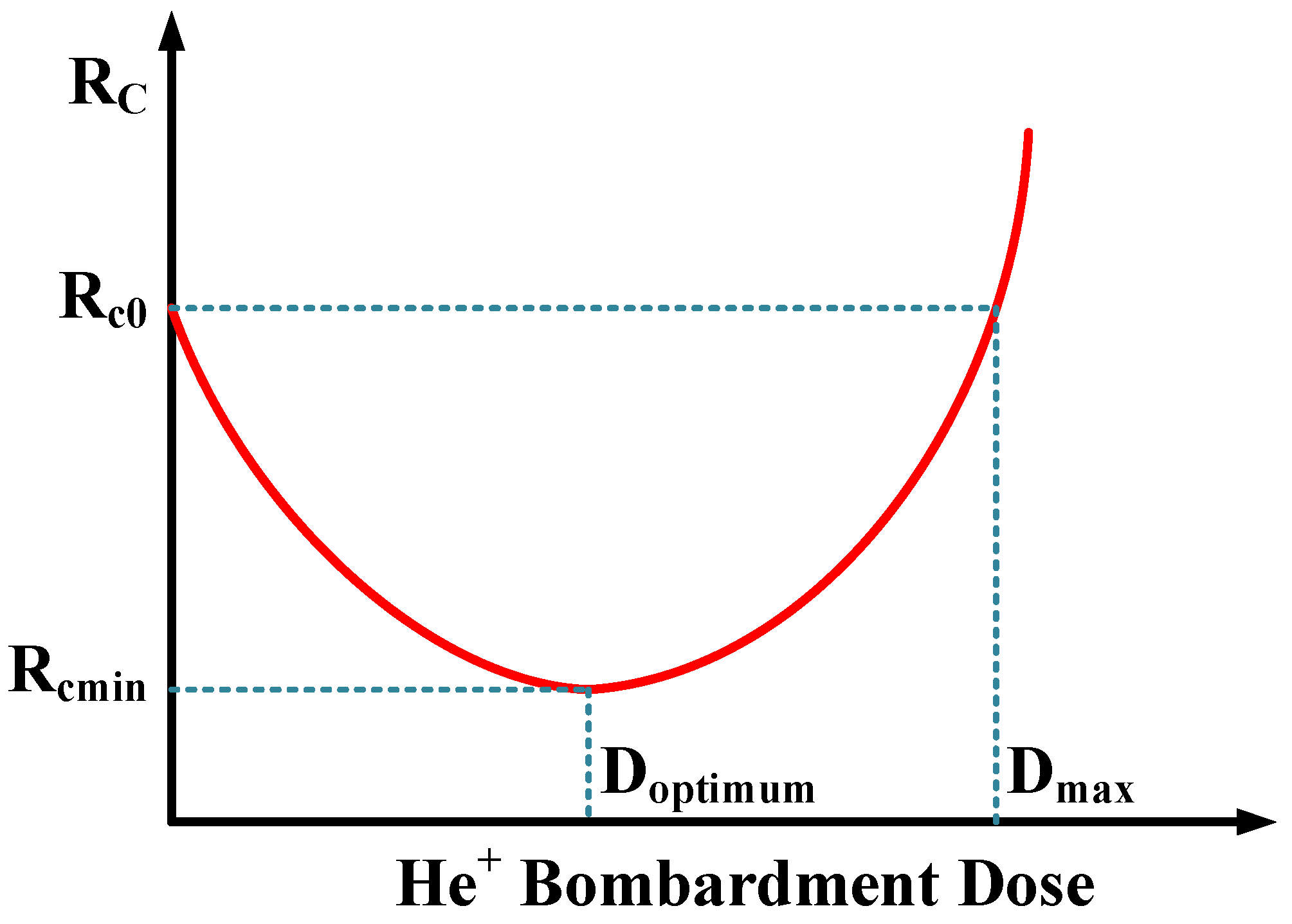
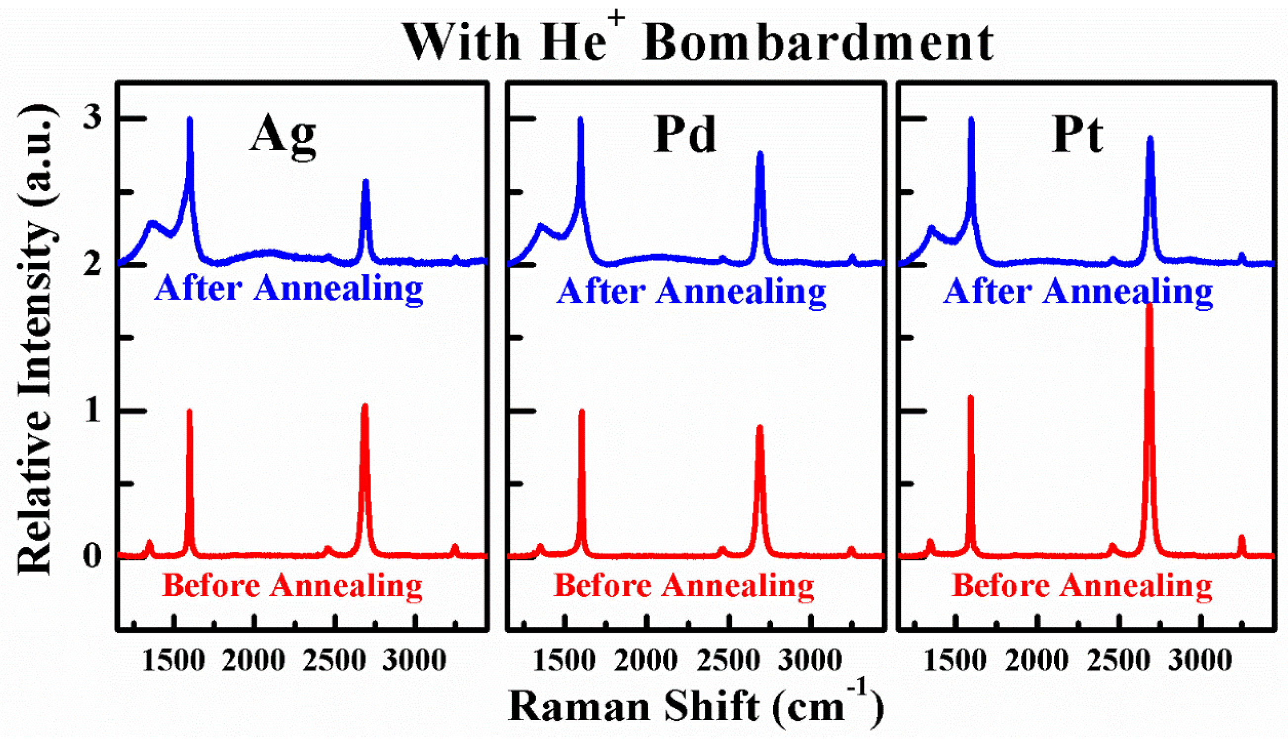
3.2. Effect of He+ Bombardment on the G-M Contact Properties
4. Conclusions
Acknowledgments
Author Contributions
Conflicts of Interest
References
- Geim, A.K. Graphene: Status and prospects. Science 2009, 324, 1530–1534. [Google Scholar] [CrossRef] [PubMed]
- Zhang, Y.; Tan, Y.-W.; Stormer, H.L.; Kim, P. Experimental observation of the quantum Hall effect and Berry’s phase in graphene. Nature 2005, 438, 201–204. [Google Scholar] [CrossRef] [PubMed]
- Hunt, B.; Sanchez-Yamagishi, J.; Young, A.; Yankowitz, M.; LeRoy, B.J.; Watanabe, K.; Taniguchi, T.; Moon, P.; Koshino, M.; Jarillo-Herrero, P. Massive Dirac fermions and Hofstadter butterfly in a van der Waals heterostructure. Science 2013, 340, 1427–1430. [Google Scholar] [CrossRef] [PubMed]
- Xia, F.; Mueller, T.; Lin, Y.-M.; Valdes-Garcia, A.; Avouris, P. Ultrafast graphene photodetector. Nat. Nanotechnol. 2009, 4, 839–843. [Google Scholar] [CrossRef] [PubMed]
- Novoselov, K.S.; Geim, A.K.; Morozov, S.; Jiang, D.; Zhang, Y.; Dubonos, S.A.; Grigorieva, I.; Firsov, A. Electric field effect in atomically thin carbon films. Science 2004, 306, 666–669. [Google Scholar] [CrossRef] [PubMed]
- Lin, Y.-M.; Dimitrakopoulos, C.; Jenkins, K.A.; Farmer, D.B.; Chiu, H.-Y.; Grill, A.; Avouris, P. 100-GHz transistors from wafer-scale epitaxial graphene. Science 2010, 327. [Google Scholar] [CrossRef] [PubMed]
- Tombros, N.; Jozsa, C.; Popinciuc, M.; Jonkman, H.T.; van Wees, B.J. Electronic spin transport and spin precession in single graphene layers at room temperature. Nature 2007, 448, 571–574. [Google Scholar] [CrossRef] [PubMed]
- Li, J.; Östling, M. Scalable Fabrication of 2D Semiconducting Crystals for Future Electronics. Electronics 2015, 4, 1033–1061. [Google Scholar] [CrossRef]
- Nagashio, K.; Nishimura, T.; Kita, K.; Toriumi, A. Metal/graphene contact as a performance killer of ultra-high mobility graphene analysis of intrinsic mobility and contact resistance. In Proceedings of the 2009 IEEE International Electron Devices Meeting (IEDM), Baltimore, MD, USA, 7–9 December 2009; pp. 1–4.
- Cayssol, J.; Huard, B.; Goldhaber-Gordon, D. Contact resistance and shot noise in graphene transistors. Phys. Rev. B 2009, 79. [Google Scholar] [CrossRef]
- Xia, F.; Perebeinos, V.; Lin, Y.-M.; Wu, Y.; Avouris, P. The origins and limits of metal-graphene junction resistance. Nat. Nanotechnol. 2011, 6, 179–184. [Google Scholar] [CrossRef] [PubMed]
- Huard, B.; Stander, N.; Sulpizio, J.; Goldhaber-Gordon, D. Evidence of the role of contacts on the observed electron-hole asymmetry in graphene. Phys. Rev. B 2008, 78. [Google Scholar] [CrossRef]
- Franklin, A.D.; Han, S.-J.; Bol, A.; Haensch, W. Effects of nanoscale contacts to graphene. IEEE Electron Device Lett. 2011, 32, 1035–1037. [Google Scholar] [CrossRef]
- Nagashio, K.; Toriumi, A. Density-of-states limited contact resistance in graphene field-effect transistors. Jpn. J. Appl. Phys. 2011, 50. [Google Scholar] [CrossRef]
- Russo, S.; Craciun, M.; Yamamoto, M.; Morpurgo, A.; Tarucha, S. Contact resistance in graphene-based devices. Phys. E 2010, 42, 677–679. [Google Scholar] [CrossRef]
- Giovannetti, G.; Khomyakov, P.; Brocks, G.; Karpan, V.; van den Brink, J.; Kelly, P. Doping graphene with metal contacts. Phys. Rev. Lett. 2008, 101. [Google Scholar] [CrossRef] [PubMed]
- Lee, E.J.; Balasubramanian, K.; Weitz, R.T.; Burghard, M.; Kern, K. Contact and edge effects in graphene devices. Nat. Nanotechnol. 2008, 3, 486–490. [Google Scholar] [CrossRef] [PubMed]
- Venugopal, A.; Colombo, L.; Vogel, E. Contact resistance in few and multilayer graphene devices. Appl. Phys. Lett. 2010, 96. [Google Scholar] [CrossRef]
- Ran, Q.; Gao, M.; Guan, X.; Wang, Y.; Yu, Z. First-principles investigation on bonding formation and electronic structure of metal-graphene contacts. Appl. Phys. Lett. 2009, 94. [Google Scholar] [CrossRef]
- Song, S.M.; Kim, T.Y.; Sul, O.J.; Shin, W.C.; Cho, B.J. Improvement of graphene-metal contact resistance by introducing edge contacts at graphene under metal. Appl. Phys. Lett. 2014, 104. [Google Scholar] [CrossRef]
- Wang, Q.; Che, J. Origins of distinctly different behaviors of Pd and Pt contacts on graphene. Phys. Rev. Lett. 2009, 103. [Google Scholar] [CrossRef] [PubMed]
- Choi, M.S.; Lee, S.H.; Yoo, W.J. Plasma treatments to improve metal contacts in graphene field effect transistor. J. Appl. Phys. 2011, 110. [Google Scholar] [CrossRef]
- Robinson, J.A.; LaBella, M.; Zhu, M.; Hollander, M.; Kasarda, R.; Hughes, Z.; Trumbull, K.; Cavalero, R.; Snyder, D. Contacting graphene. Appl. Phys.Lett. 2011, 98. [Google Scholar] [CrossRef]
- Chen, C.W.; Ren, F.; Chi, G.-C.; Hung, S.-C.; Huang, Y.; Kim, J.; Kravchenko, I.I.; Pearton, S.J. UV ozone treatment for improving contact resistance on graphene. J. Vac. Sci. Technol. B 2012, 30. [Google Scholar] [CrossRef]
- Li, W.; Hacker, C.A.; Cheng, G.; Liang, Y.; Tian, B.; Walker, A.H.; Richter, C.A.; Gundlach, D.J.; Liang, X.; Peng, L. Highly reproducible and reliable metal/graphene contact by ultraviolet-ozone treatment. J. Appl. Phys. 2014, 115. [Google Scholar] [CrossRef]
- Matsuda, Y.; Deng, W.-Q.; Goddard, W.A. Contact Resistance for “End-Contacted” Metal-Graphene and Metal-Nanotube Interfaces from Quantum Mechanics. J. Phys. Chem. C 2010, 114, 17845–17850. [Google Scholar] [CrossRef]
- Leong, W.S.; Gong, H.; Thong, J.T. Low-Contact-Resistance Graphene Devices with Nickel-Etched-Graphene Contacts. ACS Nano 2013, 8, 994–1001. [Google Scholar] [CrossRef] [PubMed]
- Smith, J.T.; Franklin, A.D.; Farmer, D.B.; Dimitrakopoulos, C.D. Reducing contact resistance in graphene devices through contact area patterning. ACS Nano 2013, 7, 3661–3667. [Google Scholar] [CrossRef] [PubMed]
- Balci, O.; Kocabas, C. Rapid thermal annealing of graphene-metal contact. Appl. Phys. Lett. 2012, 101. [Google Scholar] [CrossRef]
- Leong, W.S.; Nai, C.T.; Thong, J.T. What Does Annealing Do to Metal-Graphene Contacts? Nano Lett. 2014, 14, 3840–3847. [Google Scholar] [CrossRef] [PubMed]
- Li, X.; Cai, W.; An, J.; Kim, S.; Nah, J.; Yang, D.; Piner, R.; Velamakanni, A.; Jung, I.; Tutuc, E. Large-area synthesis of high-quality and uniform graphene films on copper foils. Science 2009, 324, 1312–1314. [Google Scholar] [CrossRef] [PubMed]
- Mattevi, C.; Kim, H.; Chhowalla, M. A review of chemical vapour deposition of graphene on copper. J. Mater. Chem. 2011, 21, 3324–3334. [Google Scholar] [CrossRef]
- Jia, K.; Luo, J.; Hu, R.; Zhan, J.; Cao, H.; Su, Y.; Zhu, H.; Xie, L.; Zhao, C.; Chen, D.; et al. Evaluation of PMMA Residues as a Function of Baking Temperature and a Graphene Heat-Free-Transfer Process to Reduce Them. ECS J. Solid State Sci. Technol. 2016, 5, P138–P141. [Google Scholar] [CrossRef]
- Hsu, A.; Wang, H.; Kim, K.K.; Kong, J.; Palacios, T. Impact of graphene interface quality on contact resistance and RF device performance. IEEE Electron Device Lett. 2011, 32, 1008–1010. [Google Scholar] [CrossRef]
- Michaelson, H.B. The work function of the elements and its periodicity. J. Appl. Phys. 1977, 48, 4729–4733. [Google Scholar] [CrossRef]
- Michaelson, H.B. Relation between an atomic electronegativity scale and the work function. IBM J. Res. Dev. 1978, 22, 72–80. [Google Scholar] [CrossRef]
- Watanabe, E.; Conwill, A.; Tsuya, D.; Koide, Y. Low contact resistance metals for graphene based devices. Diam. Relat. Mater. 2012, 24, 171–174. [Google Scholar] [CrossRef]
- Song, S.M.; Park, J.K.; Sul, O.J.; Cho, B.J. Determination of Work Function of Graphene under a Metal Electrode and Its Role in Contact Resistance. Nano Lett. 2012, 12, 3887–3892. [Google Scholar] [CrossRef] [PubMed]
- Lucchese, M.M.; Stavale, F.; Ferreira, E.M.; Vilani, C.; Moutinho, M.; Capaz, R.B.; Achete, C.; Jorio, A. Quantifying ion-induced defects and Raman relaxation length in graphene. Carbon 2010, 48, 1592–1597. [Google Scholar] [CrossRef]
- Cançado, L.G.; Jorio, A.; Ferreira, E.M.; Stavale, F.; Achete, C.; Capaz, R.; Moutinho, M.; Lombardo, A.; Kulmala, T.; Ferrari, A. Quantifying defects in graphene via Raman spectroscopy at different excitation energies. Nano Lett. 2011, 11, 3190–3196. [Google Scholar] [CrossRef] [PubMed]
- Liu, W.; Yu, H.; Wei, J.; Li, M. Impact of process induced defects on the contact characteristics of Ti/graphene devices. Electrochem. Solid-State Lett. 2011, 14, K67–K69. [Google Scholar] [CrossRef]
- Shatynski, S.R. The thermochemistry of transition metal carbides. Oxid. Met. 1979, 13, 105–118. [Google Scholar] [CrossRef]
- Gong, C.; McDonnell, S.; Qin, X.; Azcatl, A.; Dong, H.; Chabal, Y.J.; Cho, K.; Wallace, R.M. Realistic Metal-Graphene Contact Structures. ACS Nano 2014, 8, 642–649. [Google Scholar] [CrossRef] [PubMed]
- Politou, M.; Asselberghs, I.; Radu, I.; Conard, T.; Richard, O.; Lee, C.S.; Martens, K.; Sayan, S.; Huyghebaert, C.; Tokei, Z.; et al. Transition metal contacts to graphene. Appl. Phys. Lett. 2015, 107. [Google Scholar] [CrossRef]


© 2016 by the authors; licensee MDPI, Basel, Switzerland. This article is an open access article distributed under the terms and conditions of the Creative Commons Attribution (CC-BY) license (http://creativecommons.org/licenses/by/4.0/).
Share and Cite
Jia, K.; Su, Y.; Zhan, J.; Shahzad, K.; Zhu, H.; Zhao, C.; Luo, J. Enhanced End-Contacts by Helium Ion Bombardment to Improve Graphene-Metal Contacts. Nanomaterials 2016, 6, 158. https://doi.org/10.3390/nano6090158
Jia K, Su Y, Zhan J, Shahzad K, Zhu H, Zhao C, Luo J. Enhanced End-Contacts by Helium Ion Bombardment to Improve Graphene-Metal Contacts. Nanomaterials. 2016; 6(9):158. https://doi.org/10.3390/nano6090158
Chicago/Turabian StyleJia, Kunpeng, Yajuan Su, Jun Zhan, Kashif Shahzad, Huilong Zhu, Chao Zhao, and Jun Luo. 2016. "Enhanced End-Contacts by Helium Ion Bombardment to Improve Graphene-Metal Contacts" Nanomaterials 6, no. 9: 158. https://doi.org/10.3390/nano6090158
APA StyleJia, K., Su, Y., Zhan, J., Shahzad, K., Zhu, H., Zhao, C., & Luo, J. (2016). Enhanced End-Contacts by Helium Ion Bombardment to Improve Graphene-Metal Contacts. Nanomaterials, 6(9), 158. https://doi.org/10.3390/nano6090158