
Conformal Retinal Image Sensor Based on Electrochemically Exfoliated MoS2 Nanosheets


 and
and 
Abstract
1. Introduction
2. Method
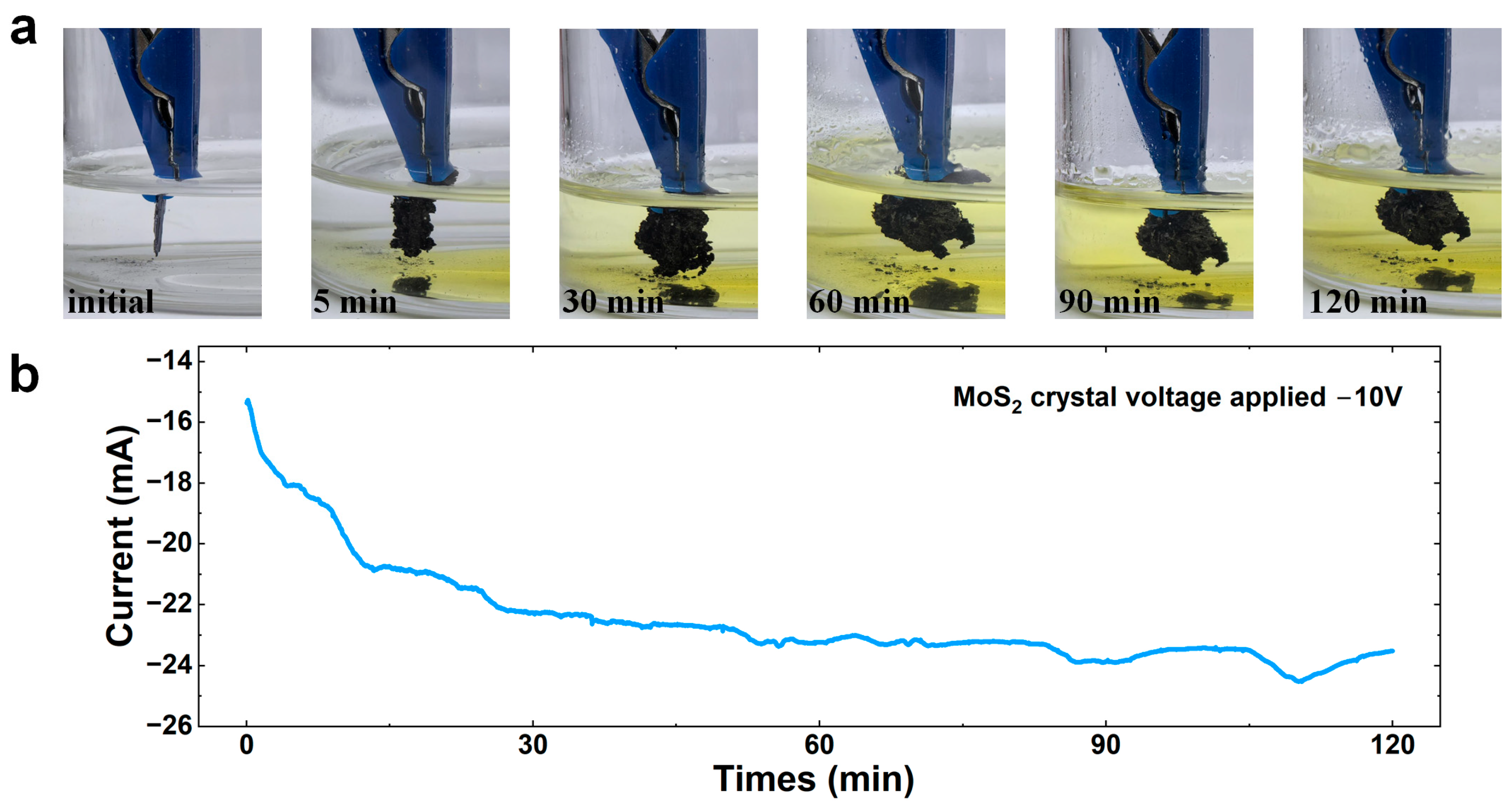
2.1. Electrochemical Exfoliation of MoS2 Crystal
2.2. Spherical Surface Disassembly and Device Fabrication
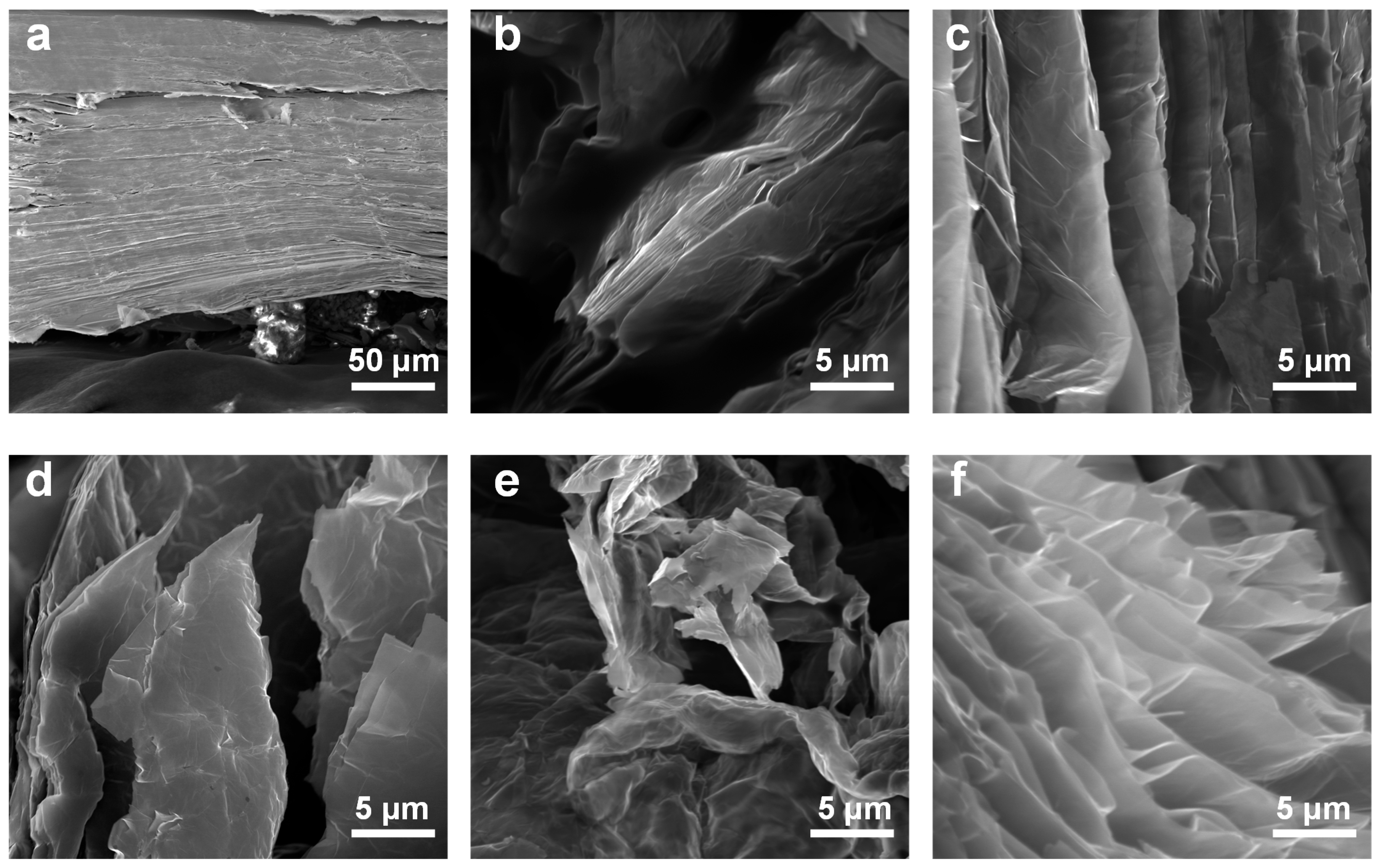
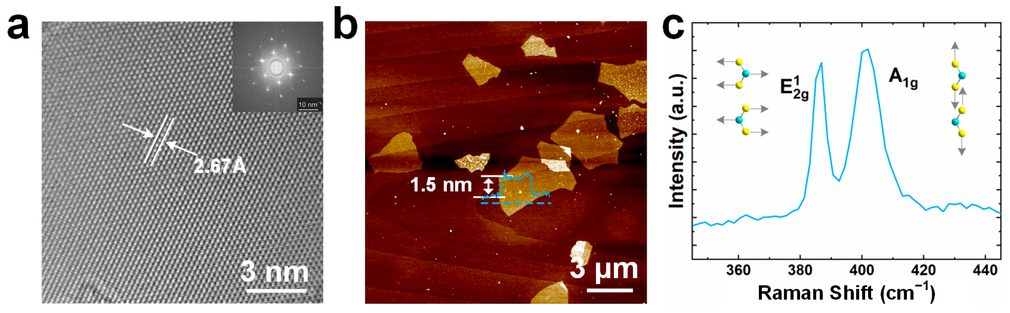
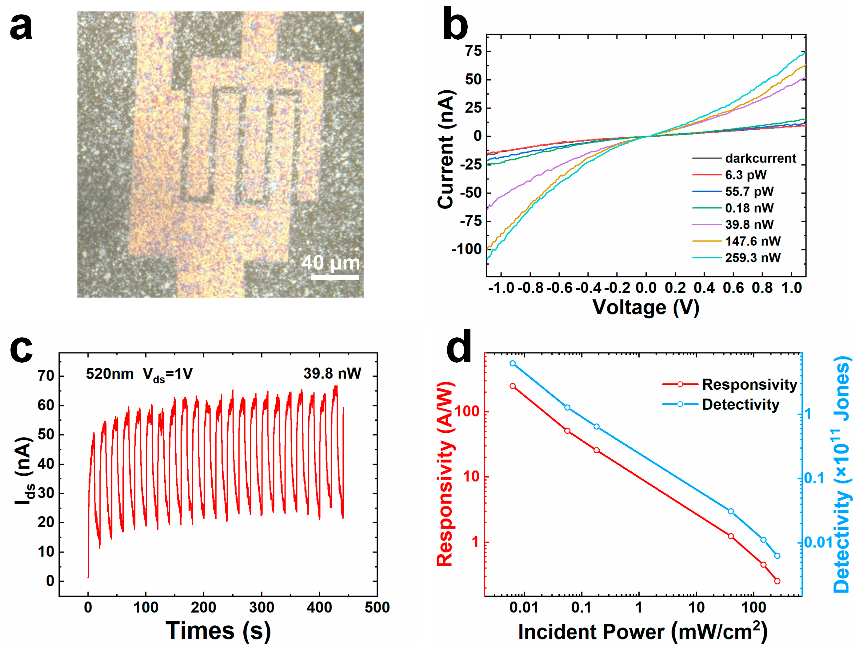
3. Result and Discussion
4. Summary
Supplementary Materials
Author Contributions
Funding
Data Availability Statement
Conflicts of Interest
References
- Lou, Z.; Shen, G. Flexible Image Sensors with Semiconducting Nanowires for Biomimic Visual Applications. Small Struct. 2021, 2, 2000152. [Google Scholar] [CrossRef]
- Choi, C.; Choi, M.K.; Liu, S.; Kim, M.S.; Park, O.K.; Im, C.; Kim, J.; Qin, X.; Lee, G.J.; Cho, K.W.; et al. Human Eye-Inspired Soft Optoelectronic Device Using High-Density MoS2-Graphene Curved Image Sensor Array. Nat. Commun. 2017, 8, 1664. [Google Scholar] [CrossRef] [PubMed]
- Debnath, S.; Roy, S.S.; Meyyappan, M.; Giri, P.K. Printed 2D WS2 Based Photodetectors and 2D MXene-Based Electromagnetic Interference Shields; IEEE: Miami, FL, USA, 2023; pp. 1–3. [Google Scholar]
- Gao, W.; Xu, Z.; Han, X.; Pan, C. Recent Advances in Curved Image Sensor Arrays for Bioinspired Vision System. Nano Today 2022, 42, 101366. [Google Scholar] [CrossRef]
- Li, H.; Yu, H.; Wu, D.; Sun, X.; Pan, L. Recent Advances in Bioinspired Vision Sensor Arrays Based on Advanced Optoelectronic Materials. APL Mater. 2023, 11, 080601. [Google Scholar] [CrossRef]
- Wu, W.; Wang, C.; Han, S.; Pan, C. Recent Advances in Imaging Devices: Image Sensors and Neuromorphic Vision Sensors. Rare Met. 2024, 43, 5487–5515. [Google Scholar] [CrossRef]
- Ko, H.C.; Stoykovich, M.P.; Song, J.; Malyarchuk, V.; Choi, W.M.; Yu, C.; Geddes, J.B., III; Xiao, J.; Wang, S.; Huang, Y.; et al. A Hemispherical Electronic Eye Camera Based on Compressible Silicon Optoelectronics. Nature 2008, 454, 748–753. [Google Scholar] [CrossRef]
- Sim, K.; Chen, S.; Li, Z.; Rao, Z.; Liu, J.; Lu, Y.; Jang, S.; Ershad, F.; Chen, J.; Xiao, J.; et al. Three-Dimensional Curvy Electronics Created Using Conformal Additive Stamp Printing. Nat. Electron. 2019, 2, 471–479. [Google Scholar] [CrossRef]
- Zhang, K.; Jung, Y.H.; Mikael, S.; Seo, J.; Kim, M.; Mi, H.; Zhou, H.; Xia, Z.; Zhou, W.; Gong, S.; et al. Origami Silicon Optoelectronics for Hemispherical Electronic Eye Systems. Nat. Commun. 2017, 8, 1782. [Google Scholar] [CrossRef]
- Lee, E.K.; Baruah, R.K.; Leem, J.W.; Park, W.; Kim, B.H.; Urbas, A.; Ku, Z.; Kim, Y.L.; Alam, M.A.; Lee, C.H. Fractal Web Design of a Hemispherical Photodetector Array with Organic-Dye-Sensitized Graphene Hybrid Composites. Adv. Mater. 2020, 32, 2004456. [Google Scholar] [CrossRef]
- Hu, Y.; Dai, M.; Feng, W.; Zhang, X.; Gao, F.; Zhang, S.; Tan, B.; Zhang, J.; Shuai, Y.; Fu, Y.; et al. Ultralow Power Optical Synapses Based on MoS2 Layers by Indium-Induced Surface Charge Doping for Biomimetic Eyes. Adv. Mater. 2021, 33, 2104960. [Google Scholar] [CrossRef]
- Gu, L.; Poddar, S.; Lin, Y.; Long, Z.; Zhang, D.; Zhang, Q.; Shu, L.; Qiu, X.; Kam, M.; Javey, A.; et al. A Biomimetic Eye with a Hemispherical Perovskite Nanowire Array Retina. Nature 2020, 581, 278–282. [Google Scholar] [CrossRef] [PubMed]
- Wu, Y.; Deng, W.; Wang, X.; Yu, W.; Chen, Z.; Chen, X.; Li, J.; Chai, Y.; Zhang, Y. Progress in Bioinspired Photodetectors Design for Visual Information Processing. Adv. Funct. Mater. 2023, 33, 2302899. [Google Scholar] [CrossRef]
- Lee, W.; Liu, Y.; Lee, Y.; Sharma, B.K.; Shinde, S.M.; Kim, S.D.; Nan, K.; Yan, Z.; Han, M.; Huang, Y.; et al. Two-Dimensional Materials in Functional Three-Dimensional Architectures with Applications in Photodetection and Imaging. Nat. Commun. 2018, 9, 1417. [Google Scholar] [CrossRef] [PubMed]
- Liu, J.; Jiang, S.; Xiong, W.; Zhu, C.; Li, K.; Huang, Y. Self-Healing Kirigami Assembly Strategy for Conformal Electronics. Adv. Funct. Mater. 2022, 32, 2109214. [Google Scholar] [CrossRef]
- Li, N.; Wang, Q.; Shen, C.; Wei, Z.; Yu, H.; Zhao, J.; Lu, X.; Wang, G.; He, C.; Xie, L.; et al. Large-Scale Flexible and Transparent Electronics Based on Monolayer Molybdenum Disulfide Field-Effect Transistors. Nat. Electron. 2020, 3, 711–717. [Google Scholar] [CrossRef]
- Chen, X.; Yang, X.; Lou, Q.; Zhang, Y.; Chen, Y.; Lu, Y.; Dong, L.; Shan, C. Fabry-Perot Interference and Piezo-Phototronic Effect Enhanced Flexible MoS2 Photodetector. Nano Res. 2022, 15, 4395–4402. [Google Scholar] [CrossRef]
- Kong, L.; Wang, S.; Su, Q.; Liu, Z.; Liao, G.; Sun, B.; Shi, T. Printed Two-Dimensional Materials for Flexible Photodetectors: Materials, Processes, and Applications. Sensors 2025, 25, 1042. [Google Scholar] [CrossRef]
- Bertolazzi, S.; Brivio, J.; Kis, A. Stretching and Breaking of Ultrathin MoS2. ACS Nano 2011, 5, 9703–9709. [Google Scholar] [CrossRef]
- Vashishtha, P.; Prajapat, P.; Sharma, A.; Goswami, P.; Walia, S.; Gupta, G. Self-Driven and Thermally Resilient Highly Responsive Nano-Fenced MoS2 Based Photodetector for Near-Infrared Optical Signal. Mater. Res. Bull. 2023, 164, 112260. [Google Scholar] [CrossRef]
- Lin, Z.; Liu, Y.; Halim, U.; Ding, M.; Liu, Y.; Wang, Y.; Jia, C.; Chen, P.; Duan, X.; Wang, C.; et al. Solution-Processable 2D Semiconductors for High-Performance Large-Area Electronics. Nature 2018, 562, 254–258. [Google Scholar] [CrossRef]
- Shi, H.; Li, M.; Shaygan Nia, A.; Wang, M.; Park, S.; Zhang, Z.; Lohe, M.R.; Yang, S.; Feng, X. Ultrafast Electrochemical Synthesis of Defect-Free in2Se3 Flakes for Large-Area Optoelectronics. Adv. Mater. 2020, 32, 1907244. [Google Scholar] [CrossRef] [PubMed]
- Yu, W.; Dong, Z.; Abdelwahab, I.; Zhao, X.; Shi, J.; Shao, Y.; Li, J.; Hu, X.; Li, R.; Ma, T.; et al. High-Yield Exfoliation of Monolayer 1T’-MoTe2 as Saturable Absorber for Ultrafast Photonics. ACS Nano 2021, 15, 18448–18457. [Google Scholar] [CrossRef] [PubMed]
- Martinez-Jodar, A.; Villar-Rodil, S.; Munuera, J.M.; Castro-Muniz, A.; Coleman, J.N.; Raymundo-Pinero, E.; Paredes, J.I. Two-Dimensional MoS2 Nanosheets Derived From Cathodic Exfoliation for Lithium Storage Applications. Nanomaterials 2024, 14, 932. [Google Scholar] [CrossRef] [PubMed]
- Wilson, N.D.; Ozhukil Valappil, M.; Martin, B.Y.; Siu, T.; Pennings, J.; Mackintosh, M.; Almadhoun, M.N.; Ouyang, J.; Graddage, N.; Pope, M.A. Toward Scalable Electrochemical Exfoliation of Molybdenum Disulfide Powder through an Accessible Electrode Design. Small Methods 2024, 9, 2400298. [Google Scholar] [CrossRef]
- Kong, L.; Li, G.; Su, Q.; Zhang, X.; Liu, Z.; Liao, G.; Sun, B.; Shi, T. Inkjet-Printed, Large-Area, Flexible Photodetector Array Based on Electrochemical Exfoliated MoS2 Film for Photoimaging. Adv. Eng. Mater. 2023, 25, 2200946. [Google Scholar] [CrossRef]
- Seo, W.; Park, W.; Seo, H.Y.; Oh, S.; Kwon, O.; Jeong, S.H.; Kim, D.H.; Kim, M.J.; Lee, S.K.; Lee, B.H.; et al. MoS2/P-Si Heterojunction with Graphene Interfacial Layer for High Performance 940 Nm Infrared Photodetector. Appl. Surf. Sci. 2022, 604, 154485. [Google Scholar] [CrossRef]
- Rahmati, B.; Hajzadeh, I.; Taheri, M.; Karimzadeh, R.; Mohajerzadeh, S.; Mohseni, S.M. Plasmonic Improvement Photoresponse of Vertical-MoS2 Nanostructure Photodetector by Au Nanoparticles. Appl. Surf. Sci. 2019, 490, 165–171. [Google Scholar] [CrossRef]
- Prajapat, P.; Vashishtha, P.; Gupta, G. Gas-Modulated Optoelectronic Properties of Monolayer MoS2 for Photodetection Applications. APL Energy 2024, 2, 046103. [Google Scholar] [CrossRef]
- Gong, C.; Colombo, L.; Wallace, R.M.; Cho, K. The Unusual Mechanism of Partial Fermi Level Pinning at Metal-MoS2 Interfaces. Nano Lett. 2014, 14, 1714–1720. [Google Scholar] [CrossRef]
- Kwon, J.; Lee, J.; Yu, Y.; Lee, C.; Cui, X.; Hone, J.; Lee, G. Thickness-Dependent Schottky Barrier Height of MoS2 Field-Effect Transistors. Nanoscale 2017, 9, 6151–6157. [Google Scholar] [CrossRef]
- Vashishtha, P.; Abidi, I.H.; Giridhar, S.P.; Verma, A.K.; Prajapat, P.; Bhoriya, A.; Murdoch, B.J.; Tollerud, J.O.; Xu, C.; Davis, J.A.; et al. CVD-Grown Monolayer MoS2 and GaN Thin Film Heterostructure for a Self-Powered and Bidirectional Photodetector with an Extended Active Spectrum. ACS Appl. Mater. Inter. 2024, 16, 31294–31303. [Google Scholar] [CrossRef] [PubMed]
- Kind, H.; Yan, H.Q.; Messer, B.; Law, M.; Yang, P.D. Nanowire Ultraviolet Photodetectors and Optical Switches. Adv. Mater. 2002, 14, 158–160. [Google Scholar] [CrossRef]
- Yu, W.; Li, S.; Zhang, Y.; Ma, W.; Sun, T.; Yuan, J.; Fu, K.; Bao, Q. Near-Infrared Photodetectors Based on MoTe2/Graphene Heterostructure with High Responsivity and Flexibility. Small 2017, 13, 1700268. [Google Scholar] [CrossRef] [PubMed]
- Choi, M.S.; Qu, D.; Lee, D.; Liu, X.; Watanabe, K.; Taniguchi, T.; Yoo, W.J. Lateral MoS2 P–N Junction Formed by Chemical Doping for Use in High-Performance Optoelectronics. ACS Nano 2014, 8, 9332–9340. [Google Scholar] [CrossRef]
- Sun, Y.; Xiong, J.; Wu, X.; Gao, W.; Huo, N.; Li, J. Highly Sensitive Infrared Polarized Photodetector Enabled by Out-of-Plane PSN Architecture Composing of P-MoTe2, Semimetal-MoTe2 and N-SnSe2. Nano Res. 2022, 15, 5384–5391. [Google Scholar] [CrossRef]
- Vashishtha, P.; Goswami, L.; Jain, S.K.; Aggarwal, N.; Gupta, G. GaN-Djoser Pyramidal Self Powered UV Photodetector for Optical Signal Detection in Rugged Environments. J. Alloys Compd. 2023, 930, 167267. [Google Scholar] [CrossRef]
- Gao, W.; Zhang, S.; Zhang, F.; Wen, P.; Zhang, L.; Sun, Y.; Chen, H.; Zheng, Z.; Yang, M.; Luo, D.; et al. 2D WS2 Based Asymmetric Schottky Photodetector with High Performance. Adv. Electron. Mater. 2021, 7, 2000964. [Google Scholar] [CrossRef]
- Zhou, C.; Raju, S.; Li, B.; Chan, M.; Chai, Y.; Yang, C.Y. Self-Driven Metal-Semiconductor-Metal WSe2 Photodetector with Asymmetric Contact Geometries. Adv. Funct. Mater. 2018, 28, 1802954. [Google Scholar] [CrossRef]
- Vashishtha, P.; Prajapat, P.; Kumar, K.; Kumar, M.; Walia, S.; Gupta, G. Multiband Spectral Response Inspired by Ultra-High Responsive Thermally Stable and Self-Powered Sb2Se3/GaN Heterojunction Based Photodetector. Surf. Interfaces 2023, 42, 103376. [Google Scholar] [CrossRef]
- Pulikodan, V.K.; Muhammed, R.; Joseph, A.; Alexander, A.; Anitha, B.; Namboothiry, M.A.G. Flexible Thin-Film Photodetectors Based on Solution-Processed Molybdenum Disulphide Nanosheets. J. Mater. Res. 2022, 37, 1246–1255. [Google Scholar] [CrossRef]
- Sharma, R.; Kumar, A.; Kumari, R.; Garg, P.; Umapathy, G.; Laisharm, R.; Ojha, S.; Srivastava, R.; Sinha, O.P. A Facile Liquid-Phase, Solvent-Dependent Exfoliation of Large Scale MoS2 Nanosheets and Study of their Photoconductive Behaviour for UV-Photodetector Application. ChemistrySelect 2021, 6, 11285–11292. [Google Scholar] [CrossRef]
- Kim, J.; Kim, S.; Cho, Y.S.; Choi, M.; Jung, S.; Cho, J.H.; Whang, D.; Kang, J. Solution-Processed MoS2 Film with Functional Interfaces Via Precursor-Assisted Chemical Welding. ACS Appl. Mater. Inter. 2021, 13, 12221–12229. [Google Scholar] [CrossRef] [PubMed]
- Chauhan, B.L.; Bhakhar, S.A.; Pataniya, P.M.; Gupta, S.U.; Solanki, G.K.; Pathak, V.M.; Patel, V. Liquid-Phase Exfoliation of WSe2 Nanosheets for ITO/WSe2 Photodetector. J. Mater. Sci. Mater. Electron. 2022, 33, 10314–10322. [Google Scholar] [CrossRef]
- Kuo, L.; Sangwan, V.K.; Rangnekar, S.V.; Chu, T.C.; Lam, D.; Zhu, Z.; Richter, L.J.; Li, R.; Szydłowska, B.M.; Downing, J.R.; et al. All-Printed Ultrahigh-Responsivity MoS2 Nanosheet Photodetectors Enabled by Megasonic Exfoliation. Adv. Mater. 2022, 34, 2203772. [Google Scholar] [CrossRef]
- Noureen, S.; Rehman, S.U.; Batool, S.M.; Ali, J.; Zhang, Q.; Batool, S.S.; Wang, Y.; Li, C. Tailoring Bi2Se3 Topological Insulator for Visible-NIR Photodetectors with Schottky Contacts Using Liquid Phase Exfoliation. ACS Appl. Mater. Inter. 2024, 16, 8158–8168. [Google Scholar] [CrossRef]
- Gao, L.; Chen, H.; Wang, R.; Wei, S.; Kuklin, A.V.; Mei, S.; Zhang, F.; Zhang, Y.; Jiang, X.; Luo, Z.; et al. Ultra-Small 2D PbS Nanoplatelets: Liquid-Phase Exfoliation and Emerging Applications for Photo-Electrochemical Photodetectors. Small 2021, 17, 2005913. [Google Scholar] [CrossRef]
Disclaimer/Publisher’s Note: The statements, opinions and data contained in all publications are solely those of the individual author(s) and contributor(s) and not of MDPI and/or the editor(s). MDPI and/or the editor(s) disclaim responsibility for any injury to people or property resulting from any ideas, methods, instructions or products referred to in the content. |
© 2025 by the authors. Licensee MDPI, Basel, Switzerland. This article is an open access article distributed under the terms and conditions of the Creative Commons Attribution (CC BY) license (https://creativecommons.org/licenses/by/4.0/).
Share and Cite
Li, T.; Yuan, H.; Cai, W.; Su, Q.; Kong, L.; Sun, B.; Shi, T. Conformal Retinal Image Sensor Based on Electrochemically Exfoliated MoS2 Nanosheets. Nanomaterials 2025, 15, 622. https://doi.org/10.3390/nano15080622
Li T, Yuan H, Cai W, Su Q, Kong L, Sun B, Shi T. Conformal Retinal Image Sensor Based on Electrochemically Exfoliated MoS2 Nanosheets. Nanomaterials. 2025; 15(8):622. https://doi.org/10.3390/nano15080622
Chicago/Turabian StyleLi, Tianxiang, Hao Yuan, Wentong Cai, Qi Su, Lingxian Kong, Bo Sun, and Tielin Shi. 2025. "Conformal Retinal Image Sensor Based on Electrochemically Exfoliated MoS2 Nanosheets" Nanomaterials 15, no. 8: 622. https://doi.org/10.3390/nano15080622
APA StyleLi, T., Yuan, H., Cai, W., Su, Q., Kong, L., Sun, B., & Shi, T. (2025). Conformal Retinal Image Sensor Based on Electrochemically Exfoliated MoS2 Nanosheets. Nanomaterials, 15(8), 622. https://doi.org/10.3390/nano15080622