
Interfacial Charge Transfer Enhances Transient Surface Photovoltage in Hybrid Heterojunctions

 , , ,
, , ,
Abstract
1. Introduction
2. Materials and Methods
3. Results
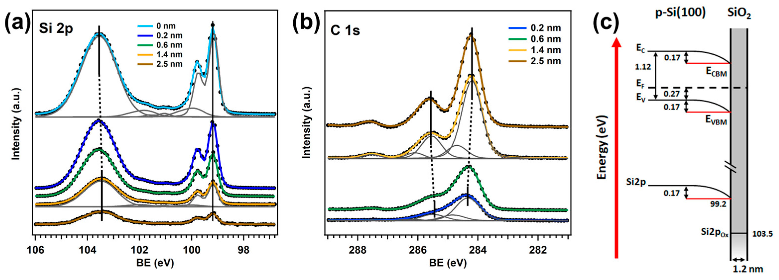
3.1. PES
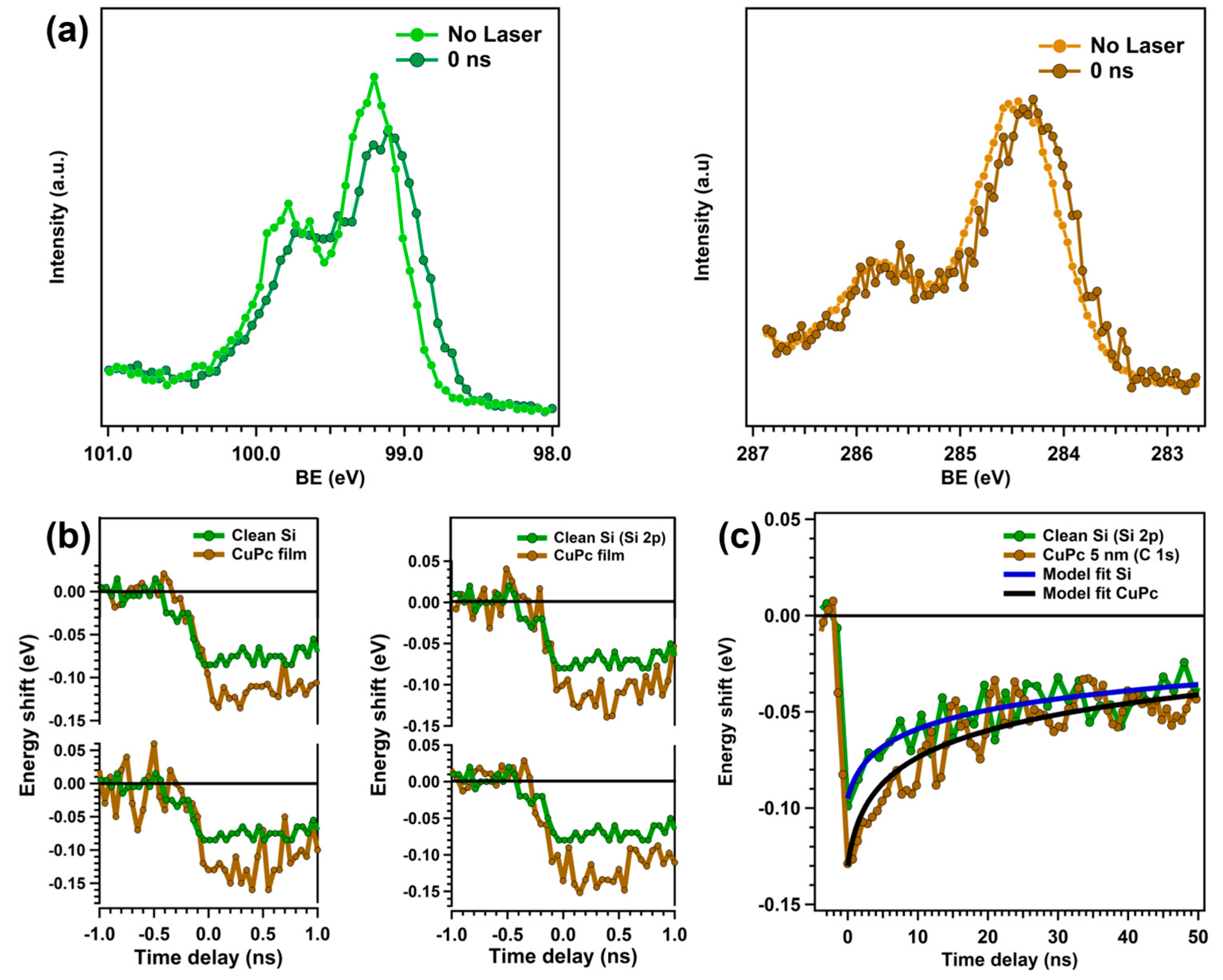
3.2. TR-PES
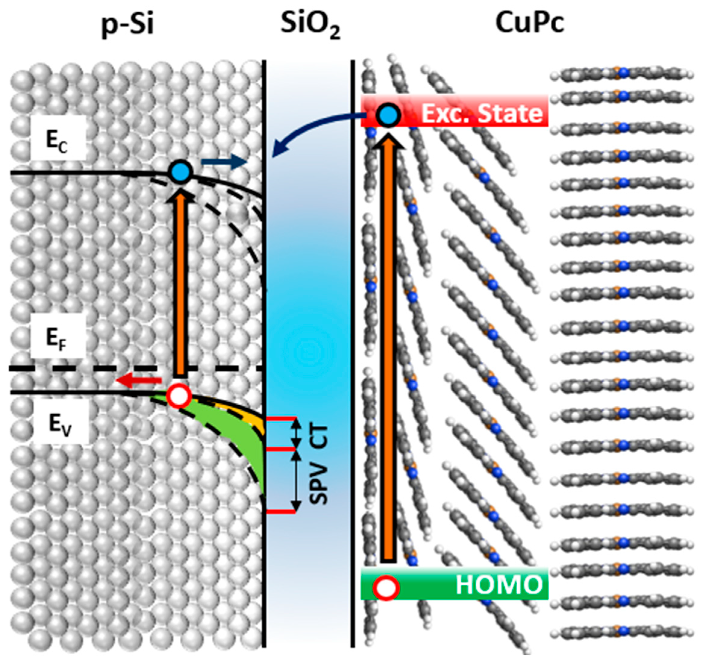
4. Discussion
5. Conclusions
Supplementary Materials
Author Contributions
Funding
Data Availability Statement
Conflicts of Interest
References
- Ishii, H.; Sugiyama, K.; Ito, E.; Seki, K. Energy Level Alignment and Interfacial Electronic Structures at Organic/Metal and Organic/Organic Interfaces. Adv. Mater. 1999, 11, 605–625. [Google Scholar] [CrossRef]
- Kronik, L.; Shapira, Y. Surface Photovoltage Spectroscopy of Semiconductor Structures: At the Crossroads of Physics, Chemistry and Electrical Engineering. Surf. Interface Anal. 2001, 31, 954–965. [Google Scholar] [CrossRef]
- Sze, S.M. Physics of Semiconductor Devices, 2nd ed.; John Wiley & Sons, Inc.: New York, NY, USA, 1981. [Google Scholar]
- Zhang, Z.; Yates, J.T. Band Bending in Semiconductors: Chemical and Physical Consequences at Surfaces and Interfaces. Chem. Rev. 2012, 112, 5520–5551. [Google Scholar] [CrossRef] [PubMed]
- Yamane, H.; Yabuuchi, Y.; Fukagawa, H.; Kera, S.; Okudaira, K.K.; Ueno, N. Does the Molecular Orientation Induce an Electric Dipole in Cu-Phthalocyanine Thin Films? J. Appl. Phys. 2006, 99, 093705. [Google Scholar] [CrossRef]
- Peisert, H.; Knupfer, M.; Schwieger, T.; Auerhammer, J.M.; Golden, M.S.; Fink, J. Full Characterization of the Interface between the Organic Semiconductor Copper Phthalocyanine and Gold. J. Appl. Phys. 2002, 91, 4872–4878. [Google Scholar] [CrossRef]
- Peisert, H.; Schwieger, T.; Auerhammer, J.M.; Knupfer, M.; Golden, M.S.; Fink, J.; Bressler, P.R.; Mast, M. Order on Disorder: Copper Phthalocyanine Thin Films on Technical Substrates. J. Appl. Phys. 2001, 90, 466–469. [Google Scholar] [CrossRef]
- Costantini, R.; Grazioli, C.; Cossaro, A.; Floreano, L.; Morgante, A.; Dell’Angela, M. Pump-Probe X-Ray Photoemission Reveals Light-Induced Carrier Accumulation in Organic Heterojunctions. J. Phys. Chem. C 2020, 124, 26603–26612. [Google Scholar] [CrossRef]
- Liu, Y.; Park, S.H.; Kim, J. Efficient Integrated Perovskite/Organic Solar Cells via Interdigitated Interfacial Charge Transfer. ACS Appl. Mater. Interfaces 2023, 15, 34742–34749. [Google Scholar] [CrossRef]
- Roth, F.; Borgwardt, M.; Wenthaus, L.; Mahl, J.; Palutke, S.; Brenner, G.; Mercurio, G.; Molodtsov, S.; Wurth, W.; Gessner, O.; et al. Direct Observation of Charge Separation in an Organic Light Harvesting System by Femtosecond Time-Resolved XPS. Nat. Commun. 2021, 12, 1196. [Google Scholar] [CrossRef]
- Zhang, T.; Concannon, N.M.; Holmes, R.J. Migration of Charge-Transfer States at Organic Semiconductor Heterojunctions. ACS Appl. Mater. Interfaces 2020, 12, 31677–31686. [Google Scholar] [CrossRef]
- Dutton, G.J.; Robey, S.W. Exciton Dynamics at CuPc/C60 Interfaces: Energy Dependence of Exciton Dissociation. J. Phys. Chem. C 2012, 116, 19173–19181. [Google Scholar] [CrossRef]
- Reshchikov, M.A.; Foussekis, M.; Baski, A.A. Surface Photovoltage in Undoped N-Type GaN. J. Appl. Phys. 2010, 107, 113535. [Google Scholar] [CrossRef]
- Fengler, S.; Kriegel, H.; Schieda, M.; Gutzmann, H.; Klassen, T.; Wollgarten, M.; Dittrich, T. Charge Transfer in c-Si(n++)/TiO2(ALD) at the Amorphous/Anatase Transition: A Transient Surface Photovoltage Spectroscopy Study. ACS Appl. Mater. Interfaces 2020, 12, 3140–3149. [Google Scholar] [CrossRef] [PubMed]
- Dittrich, T. Transient surface photovoltage spectroscopy of diamond. AIP Adv. 2022, 12, 065206. [Google Scholar] [CrossRef]
- Bozheyev, F.; Fengler, S.; Kollmann, J.; Klassen, T.; Schieda, M. Transient Surface Photovoltage Spectroscopy of (NH4)2Mo3S13/WSe2 Thin-Film Photocathodes for Photoelectrochemical Hydrogen Evolution. ACS Appl. Mater. Interfaces 2022, 14, 22071–22081. [Google Scholar] [CrossRef]
- Pierucci, D.; Silly, M.G.; Tissot, H.; Hollander, P.; Sirotti, F.; Rochet, F. Surface Photovoltage Dynamics at Passivated Silicon Surfaces: Influence of Substrate Doping and Surface Termination. Faraday Discuss. 2022, 236, 442–460. [Google Scholar] [CrossRef]
- Bröcker, D.; Gießel, T.; Widdra, W. Charge Carrier Dynamics at the SiO2/Si(1 0 0) Surface: A Time-Resolved Photoemission Study with Combined Laser and Synchrotron Radiation. Chem. Phys. 2004, 299, 247–251. [Google Scholar] [CrossRef]
- Ogawa, M.; Yamamoto, S.; Fujikawa, K.; Hobara, R.; Yukawa, R.; Yamamoto, S.; Kitagawa, S.; Pierucci, D.; Silly, M.G.; Lin, C.H.; et al. Relaxations of the Surface Photovoltage Effect on the Atomically Controlled Semiconductor Surfaces Studied by Time-Resolved Photoemission Spectroscopy. Phys. Rev. B 2013, 88, 165313. [Google Scholar] [CrossRef]
- Çopurogìlu, M.; Sezen, H.; Opila, R.L.; Suzer, S. Band-Bending at Buried SiO2/Si Interface as Probed by XPS. ACS Appl. Mater. Interfaces 2013, 5, 5875–5881. [Google Scholar] [CrossRef]
- Grzadziel, L.; Krzywiecki, M.; Peisert, H.; Chassé, T.; Szuber, J. Photoemission Study of the Si(1 1 1)-Native SiO2/Copper Phthalocyanine (CuPc) Ultra-Thin Film Interface. Org. Electron. 2012, 13, 1873–1880. [Google Scholar] [CrossRef]
- Ruocco, A.; Evangelista, F.; Gotter, R.; Attili, A.; Stefani, G. Evidence of Charge Transfer at the Cu-Phthalocyanine/Al(100) Interface. J. Phys. Chem. C 2008, 112, 2016–2025. [Google Scholar] [CrossRef]
- Schönauer, K.; Weiss, S.; Feyer, V.; Lüftner, D.; Stadtmüller, B.; Schwarz, D.; Sueyoshi, T.; Kumpf, C.; Puschnig, P.; Ramsey, M.G.; et al. Charge Transfer and Symmetry Reduction at the CuPc/Ag(110) Interface Studied by Photoemission Tomography. Phys. Rev. B 2016, 94, 205144. [Google Scholar] [CrossRef]
- Peisert, H.; Knupfer, M.; Schwieger, T.; Fink, J. Strong Chemical Interaction between Indium Tin Oxide and Phthalocyanines. Appl. Phys. Lett. 2002, 80, 2916–2918. [Google Scholar] [CrossRef]
- Costantini, R.; Stredansky, M.; Cvetko, D.; Kladnik, G.; Verdini, A.; Sigalotti, P.; Cilento, F.; Salvador, F.; De Luisa, A.; Benedetti, D.; et al. ANCHOR-SUNDYN: A Novel Endstation for Time Resolved Spectroscopy at the ALOISA Beamline. J. Electron Spectrosc. Relat. Phenom. 2018, 229, 7–12. [Google Scholar] [CrossRef]
- Krzywiecki, M. Studies of CuPc Ultra-Thin Layers Deposited on Si(111) Native Substrates. Ph.D. Thesis, Institute of Physics–CSE, Silesian University of Technology, Gliwice, Poland, 2010. [Google Scholar]
- Costantini, R.; Faber, R.; Cossaro, A.; Floreano, L.; Verdini, A.; Hättig, C.; Morgante, A.; Coriani, S.; Dell’Angela, M. Picosecond Timescale Tracking of Pentacene Triplet Excitons with Chemical Sensitivity. Commun. Phys. 2019, 2, 56. [Google Scholar] [CrossRef]
- Papageorgiou, N.; Ferro, Y.; Salomon, E.; Allouche, A.; Layet, J.M.; Giovanelli, L.; Le Lay, G. Geometry and Electronic Structure of Lead Phthalocyanine: Quantum Calculations via Density-Functional Theory and Photoemission Measurements. Phys. Rev. B 2003, 68, 235105. [Google Scholar] [CrossRef]
- Evangelista, F.; Carravetta, V.; Stefani, G.; Jansik, B.; Alagia, M.; Stranges, S.; Ruocco, A. Electronic Structure of Copper Phthalocyanine: An Experimental and Theoretical Study of Occupied and Unoccupied Levels. J. Chem. Phys. 2007, 126, 124709. [Google Scholar] [CrossRef]
- Gorgoi, M.; Zahn, D.R.T. “band Bending” in Copper Phthalocyanine on Hydrogen-Passivated Si(1 1 1). Org. Electron. 2005, 6, 168–174. [Google Scholar] [CrossRef]
- Sai, N.; Gearba, R.; Dolocan, A.; Tritsch, J.R.; Chan, W.-L.; Chelikowsky, J.R.; Leung, K.; Zhu, X. Understanding the Interface Dipole of Copper Phthalocyanine (CuPc)/C 60: Theory and Experiment. J. Phys. Chem. Lett. 2012, 3, 2173–2177. [Google Scholar] [CrossRef]
- Long, J.P.; Sadeghi, H.R.; Rife, C.; Kabler, M.N. Surface Space-Charge Dynamics and Surface Recombination on Silicon (111) Surfaces Measured with Combined Laser and Synchrotron Radiation. Phys. Rev. Lett. 1990, 64, 1158. [Google Scholar] [CrossRef]
- Hecht, M.H. Time Dependence of Photovoltaic Shifts in Photoelectron Spectroscopy of Semiconductors. Phys. Rev. B 1991, 43, 12102–12105. [Google Scholar] [CrossRef] [PubMed]
- Baek, D.; Rouvimov, S.; Kim, B.; Jo, T.C.; Schroder, D.K. Surface Recombination Velocity of Silicon Wafers by Photoluminescence. Appl. Phys. Lett. 2005, 86, 112110. [Google Scholar] [CrossRef]
- Jailaubekov, A.E.; Willard, A.P.; Tritsch, J.R.; Chan, W.L.; Sai, N.; Gearba, R.; Kaake, L.G.; Williams, K.J.; Leung, K.; Rossky, P.J.; et al. Hot Charge-Transfer Excitons Set the Time Limit for Charge Separation at Donor/Acceptor Interfaces in Organic Photovoltaics. Nat. Mater. 2013, 12, 66–73. [Google Scholar] [CrossRef] [PubMed]
- Zhu, J.; Hayashi, H.; Chen, M.; Xiao, C.; Matsuo, K.; Aratani, N.; Zhang, L.; Yamada, H. Single crystal field-effect transistor of tetrabenzoporphyrin with a one-dimensionally extended columnar packing motif exhibiting efficient charge transport properties. J. Mater. Chem. C 2022, 10, 2527. [Google Scholar] [CrossRef]
- Lim, H.; Yang, S.; Lee, S.-H.; Lee, J.-Y.; Lee, Y.; Situmorang, A.B.; Kim, Y.-H.; Kim, J.W. Influence of the metal phthalocyanine molecular orientation on charge separation at the organic donor/acceptor interface. J. Mater. Chem. C 2021, 9, 2156–2164. [Google Scholar] [CrossRef]
- Ozawa, K.; Yamamoto, S.; Miyazawa, T.; Yano, K.; Okudaira, K.; Mase, K.; Matsuda, I. Influence of Stacking Order of Phthalocyanine and Fullerene Layers on the Photoexcited Carrier Dynamics in Model Organic Solar Cell. J. Phys. Chem. C 2021, 125, 13963–13970. [Google Scholar] [CrossRef]
- Soncini, C.; Kumar, A.; Bondino, F.; Magnano, E.; Stupar, M.; Ressel, B.; De Ninno, G.; Papadopoulos, A.; Serpetzoglou, E.; Stratakis, E.; et al. Modulation of Charge Transfer Exciton Dynamics in Organic Semiconductors using different structural arrangements. J. Mater. Chem. C 2023, 11, 10266–10273. [Google Scholar] [CrossRef]

| Thickness (nm) | Cα BE (eV) | Cα-Cβ Energy Distance (eV) | FWHM (eV) |
|---|---|---|---|
| 0.2 | 284.34 | 1.11 | 0.82 |
| 0.6 | 284.29 | 1.26 | 0.80 |
| 1.4 | 284.20 | 1.35 | 0.67 |
| 2.5 | 284.22 | 1.36 | 0.61 |
| Sample | SPV0 (meV) | Ns (cm−2) | η | Sv (cm s−1) |
|---|---|---|---|---|
| SiO2/Si(100) | −95 | 4.23 × 10¹⁰ | 0.63 | 4870 |
| CuPc/SiO2/Si(100) | −130 | 2.25 × 10¹⁰ | 0.8 | 4450 |
Disclaimer/Publisher’s Note: The statements, opinions and data contained in all publications are solely those of the individual author(s) and contributor(s) and not of MDPI and/or the editor(s). MDPI and/or the editor(s) disclaim responsibility for any injury to people or property resulting from any ideas, methods, instructions or products referred to in the content. |
© 2025 by the authors. Licensee MDPI, Basel, Switzerland. This article is an open access article distributed under the terms and conditions of the Creative Commons Attribution (CC BY) license (https://creativecommons.org/licenses/by/4.0/).
Share and Cite
Soncini, C.; Costantini, R.; Dell’Angela, M.; Morgante, A.; Pedio, M. Interfacial Charge Transfer Enhances Transient Surface Photovoltage in Hybrid Heterojunctions. Nanomaterials 2025, 15, 154. https://doi.org/10.3390/nano15030154
Soncini C, Costantini R, Dell’Angela M, Morgante A, Pedio M. Interfacial Charge Transfer Enhances Transient Surface Photovoltage in Hybrid Heterojunctions. Nanomaterials. 2025; 15(3):154. https://doi.org/10.3390/nano15030154
Chicago/Turabian StyleSoncini, Cristian, Roberto Costantini, Martina Dell’Angela, Alberto Morgante, and Maddalena Pedio. 2025. "Interfacial Charge Transfer Enhances Transient Surface Photovoltage in Hybrid Heterojunctions" Nanomaterials 15, no. 3: 154. https://doi.org/10.3390/nano15030154
APA StyleSoncini, C., Costantini, R., Dell’Angela, M., Morgante, A., & Pedio, M. (2025). Interfacial Charge Transfer Enhances Transient Surface Photovoltage in Hybrid Heterojunctions. Nanomaterials, 15(3), 154. https://doi.org/10.3390/nano15030154