2. Methodology
Three modulator structures were investigated, namely the straight bus–ring modulator, the bent bus–ring modulator, and the racetrack modulator, as illustrated in
Figure 1a–c. The core waveguide material was Si
3N
4, modeled using refractive index values corresponding to a 450 nm thick Si
3N
4 film. The parameters such as coupling efficiency, propagation loss, and graphene absorption were calculated for the transverse electric (TE) guided light mode at a wavelength of 1310 nm.
To ensure accuracy, perfectly matched layer (PML) boundary conditions were applied in the FDTD solver for coupling efficiency calculations and in the Mode solver for evaluating propagation loss. Furthermore, the graphene surface conductivity material model was utilized to accurately calculate the graphene’s absorption of the guided light mode.
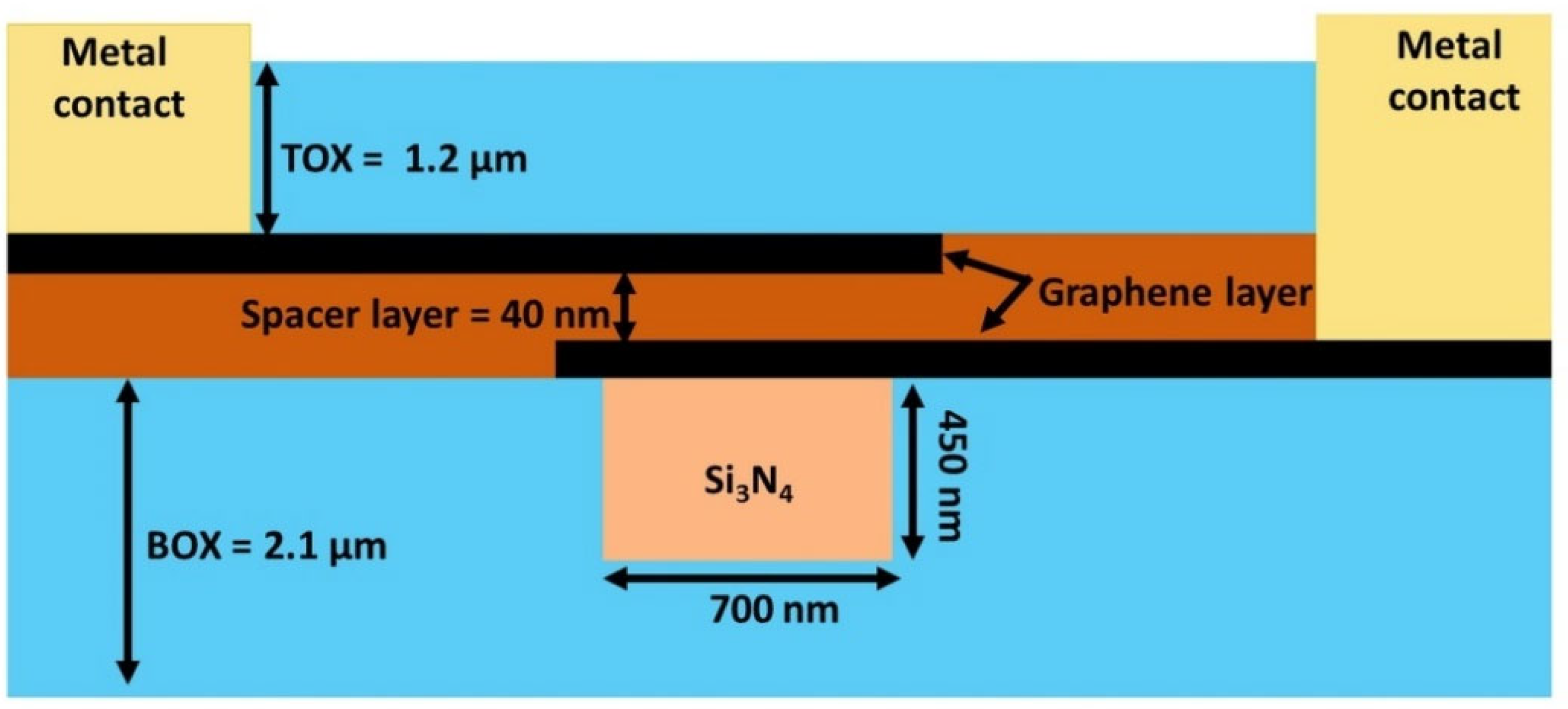
Figure 2 sketches the cross-sectional view of a bilayer graphene modulator applied to all the geometries depicted in
Figure 1. Si
3N
4 has been used as the core waveguide material, with dimensions of 450 nm in height and 750 nm in width. The top oxide (TOX) and bottom oxide (BOX) act as the cladding layer for the waveguide core, with heights of 1.2 µm and 2.1 µm, respectively. The two-graphene layers are separated by a 40 nm dielectric layer, and a gold metal electrode was employed to apply the voltage to the individual graphene layer. Practical integration of high-quality graphene on silicon nitride has been demonstrated using advanced transfer and growth techniques such as dry transfer and direct chemical vapor deposition (CVD), as explained in recent studies [
21,
22], including controlled PECVD-based dielectric deposition after surface pre-treatment and annealing, which enables compatibility with standard fabrication flows [
23,
24].
The gate voltage V is applied to these metal contacts to adjust the absorption state of the graphene layer by modulating its chemical potential μ, according to the following relation:
where ℏ is the reduced Plank constant,
is the voltage offset caused by natural doping of the graphene layer, and
The shift in the chemical potential resulting from the applied voltages changes the optical conductivity
of the graphene sheet expression, which is derived from the Kubo formalism [
25]:
where
ω is the angular frequency,
Γ is the scattering rate,
μ is the chemical potential,
T is the temperature,
e is the electron charge,
is the Boltzmann constant,
is the energy level, and
is the Fermi Dirac distribution function given by the following:
The variation in the graphene’s optical conductivity, as per Equation (2), results in variation in the dielectric constant ε. Consequently, the waveguide’s effective refractive index
n also changes, as indicated in Equation (4) below:
Here, spacer layer thickness
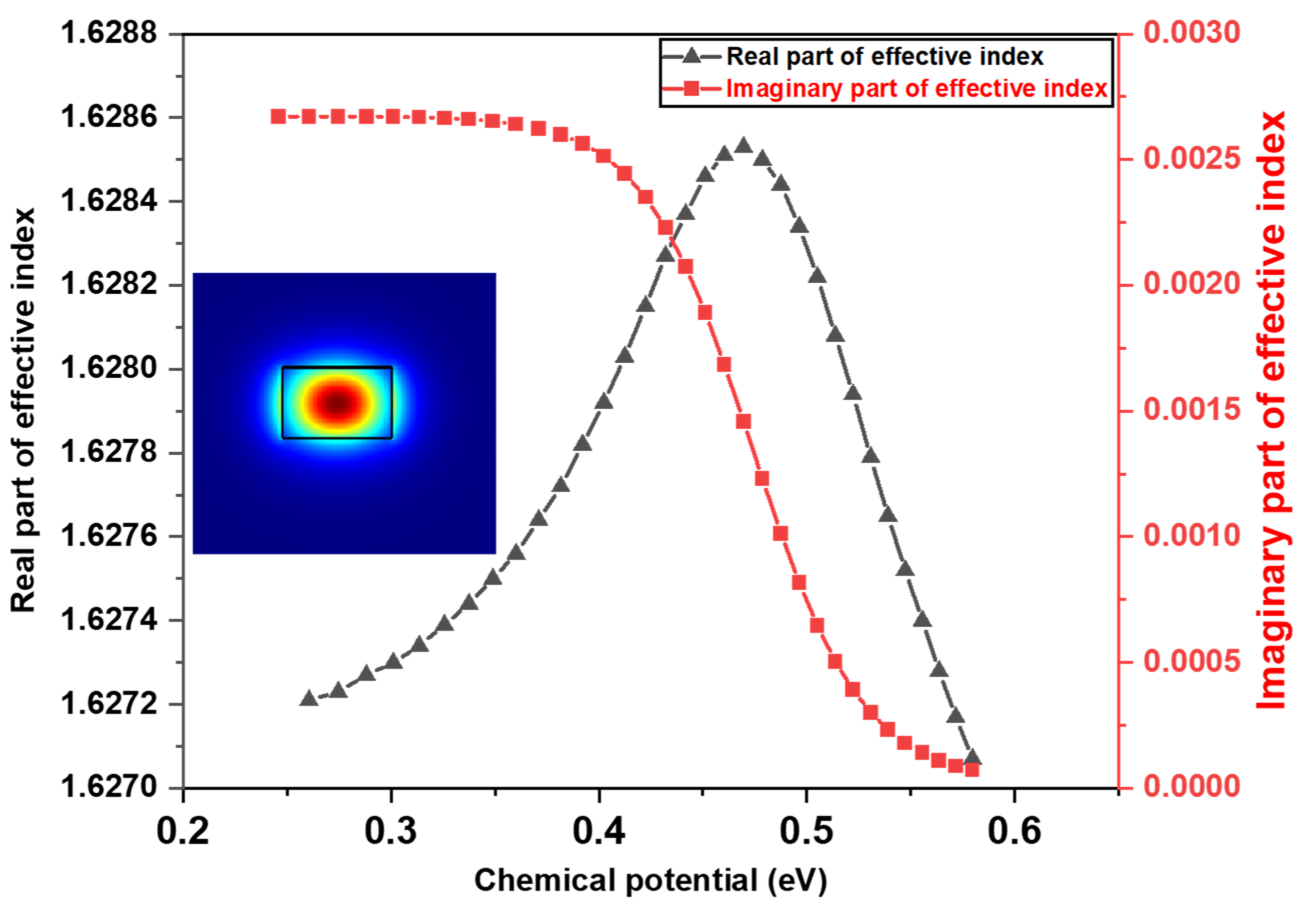
between the graphene sheets was chosen as 40 nm, which offers a balance between strong field overlap (for efficient modulation) and prevention of dielectric breakdown. Graphene was modeled as a 2D conductive sheet using the surface conductivity approach derived from the Kubo formalism. Specifically, we used Lumerical MODE’s eigenmode solver to compute the complex effective refractive index
of the graphene-integrated silicon nitride waveguide for different values of chemical potential μ (calculated from Ansys charge solver). The resulting
values were then used as input to emulate the electro-absorption modulation mechanism by varying μ as a function of applied gate voltage. The scattering rate Γ was fixed at 15 meV in all simulations, a value calculated based on experimentally derived parameters for CVD-grown graphene on silicon nitride, as reported in Wang et al. [
26]. By using the Ansys charge solver, the graphene layer’s total charge and resulting chemical potential and optical conductivity σ for Equation (4) were calculated. These values are then utilized to compute the effective refractive index of the graphene-integrated silicon nitride waveguide as shown in Equation (3). In
Figure 3, the variation in the real and imaginary components of the effective index for a graphene-on-silicon nitride waveguide system as a function of the chemical potential for TE mode (mode profile is shown in the inset) is plotted. These values were obtained using a mode solver’s finite-difference eigenmode (FDE) simulations. The extracted parameters were subsequently utilized to estimate the propagation loss in the waveguide due to the graphene’s absorption.
3. Results and Discussion
Using an FDTD eigen mode solver, the bending loss of the micro ring was first analyzed to design a resonator radius that provides an optimal balance between minimal radiation loss and a compact device footprint. Such a loss arises due to the tight curvature pushing the guided mode away from the waveguide’s high-index core; the resulting phase mismatch lets energy radiate into the surrounding cladding, so smaller radii leak light and degrade as it propagates in the waveguide core [
27]. Simulations were carried out for the fundamental TE mode at λ = 1310 nm. The bend radius was swept from 10 µm to 50 µm while all other waveguide dimensions remained fixed. The resulting attenuation, plotted in
Figure 4a, drops exponentially with the radius of the ring. Propagation losses remain below 0.2 dB/cm for a ring radius of 30 µm and become negligibly small beyond 40 µm. Based on this observation, a radius of r = 40 μm is selected for all subsequent designs, as it effectively suppresses radiation losses while preserving a suitable free spectral range for modulation and maintaining a compact device footprint. Secondly, metal-induced loss was evaluated by analyzing the overlap between the evanescent tail of the guided TE mode and the lossy metal electrodes [
28]. The metal–waveguide separation ‘g’ (as illustrated in the inset of
Figure 4b) serves as a critical design parameter, as it simultaneously influences the device’s electrical bandwidth and the optical loss induced by the metal. Reducing the gap lowers the overall resistance capacitance (RC) time constant and therefore extends the device’s electrical bandwidth; however, bringing the metal too close to the waveguide also increases parasitic absorption in the ring. An eigenmode solver was used to model two 360 nm thick gold (Au) metal contacts placed on either side of the waveguide (see
Figure 4b, inset), with their lateral separation g swept from 0.5 µm to 1.4 µm. At g = 0.5 µm, the evanescent tail overlaps strongly with the metal, adding additional absorption of ≈0.15 dB/µm. The absorption decreases rapidly with the increase in distance ‘g’, and the value reaches 0.02 dB/µm at g = 0.7 µm, dropping below 0.01 dB/µm once the electrodes are ≥0.8 µm apart. Positioning the electrodes at least 0.8 µm from the core limits metal-induced attenuation to <0.01 dB/µm while maintaining a sufficiently smaller metal–graphene distance for high electrical bandwidth of the device.
Moreover, the bus–ring power coupling efficiency
was subsequently evaluated, where
corresponds to complete power transfer between the waveguide and the ring (output bus transmission T = 0). This parameter is tunable via the gap between the ring and the bus waveguide. A FDTD simulation for three evanescent-coupled resonator layouts—a straight bus waveguide adjacent to a circular ring (
Figure 5a), a bent bus waveguide coupled to the ring (
Figure 5b), and a racetrack resonator with a straight coupling section (
Figure 5c)—were conducted. Adapting the standard formulation of coupled mode theory for two weakly coupled, phase-matched optical waveguides [
29,
30], the slowly varying field envelopes in the bus, a(z), and in the ring, b(z), can be written as follows:
where a and b are the normalized complex amplitude of the guided mode (travelling along z) in the bus and ring, respectively, and β is the propagation constant. The per length coupling constant falls off almost exponentially with the bus–ring gap d as
with
is evanescent-field decay length into the cladding. Integrating Equation (5) over the physical interaction length L gives the following complex field-transfer coefficient:
and the power-coupling efficiency is given by
. In the common phase-matched
= 0, the coupling efficiency is given by the following:
Here, the only geometry-dependent parameter is the interaction length or the coupling length L. For the straight bus coupled to the ring, the coupling length
is shorter in comparison to the bent bus coupling length
= r
and the racetrack coupling length
. Although the bent bus coupler offers a nominally longer interaction length (
= R ×
= 26 μm) for a 40 µm radius ring and an arc angle of 34° (
Figure 5b), its power-coupling efficiency is nonetheless lower than that of the racetrack, whose straight coupling section is only 20 μm (
Figure 5d). This can be explained by the coupled-mode expression (Equation (6)), showing that coupling efficiency depends not on length alone but on the combined product
and L and the phase-mismatch penalty
. In the bent bus, the curved waveguide’s mode maximum is located further from the ring core, so the per-length coupling coefficient
is intrinsically smaller than in the parallel, straight-guide section of the racetrack. Curvature also introduces a non-zero propagation-constant difference Δβ =
, further suppressing the overall coupling efficiency relative to the racetrack coupling design. For each geometry shown in
Figure 5, the bus–ring coupling gap separation
was swept from 100 nm to 500 nm, with the ring radius fixed at
r = 40 µm. In the 2D finite-difference time-domain (FDTD) simulation, a power monitor is placed inside the micro-ring resonator. A broadband Gaussian pulse centered at a wavelength of 1310 nm with TE polarization is injected, and the resulting spectral response of the light confined within the ring is recorded.
Figure 5d compares the coupling efficiencies for a 40 µm ring radius across all resonator geometries, depicting how each design—straight bus, bent bus, and racetrack—performs at the same ring radius. Overall, the results show that the straight and bent bus waveguide configurations achieve their highest coupling efficiency at moderate gaps (roughly 100–200 nm), whereas the racetrack design maintains more significant coupling efficiency at larger gaps (250–300 nm). Consequently, while smaller gaps are necessary to sustain strong coupling in the straight and bent bus geometries, a racetrack-based modulator design can still achieve high efficiency at gaps of 250 nm and beyond. This understanding is crucial, as coupling efficiency directly determines the resonator’s transmission characteristics, a key parameter for the operation of a ring modulator.
The working principle of the graphene-integrated ring modulator is described using all-pass ring resonator formalism [
31,
32], which relates the input complex field amplitude
and output complex field amplitude
as shown in the inset of
Figure 6a. Here, α is the round-trip loss coefficient of the ring, and t is the self-coupling coefficient of the ring–bus system. The former is fixed by the bus–ring coupling gap and length
, whereas the latter is tuned electrically by changing the graphene absorption with gate voltage or tuning the graphene length itself. Assuming lossless coupling such that |
, where κ is the cross-coupling coefficient, the normalized bus output transmission T at resonance is given by the following:
From Equation (8), it is evident that bus output transmission T is governed solely by the interplay between α and t.
When the above condition is satisfied, the numerator in Equation (8) vanishes and total destructive interference leads to zero output bus transmission T, i.e., the critically coupled condition. On the other hand, when α→1, representing a nearly lossless ring (e.g., when graphene becomes highly transparent), the denominator dominates, and the bus transmission approaches unity.
This dynamic range in T, tunable via the gate-controlled modulation of α, enables effective intensity modulation. Therefore, by co-designing the coupling parameters (i.e., ring radius, coupling gap, and coupling length) and the graphene bias range, one can ensure the system reaches the critical coupling condition required to achieve high modulation depth in graphene ring modulators. Following this ring resonator theory, a graphene ring modulator with a straight bus was modeled in the simulation. The purpose is to study the output bus transmission with different graphene length sections on the ring circumference (inset of
Figure 6a). In the simulations, only the magnitude of the coupling coefficient (
) is used as an input parameter, based on frequency-dependent mode overlap characteristics imported from FDTD eigenmode solvers. For this reason, the results in
Figure 6a were plotted only for the straight bus–ring configuration, as it sufficiently captures the dependence of extinction behavior on coupling gap parameter
κ2 and the graphene length via the effective loss parameter α, without loss of generality across the other structures [
33]. At first the graphene layer was gate-tuned to a chemical potential of 0 eV, placing it in a high conductivity state. This condition effectively rendered the graphene to an absorptive state, with a non-zero imaginary component of the effective index (as shown in
Figure 3).
Figure 6a presents the simulated bus transmission
T at different coupling efficiency
κ2 for various graphene lengths integrated on a ring with a 40 µm radius coupled to a straight bus waveguide. The transmission exhibits the minimum value for a specific value of
κ2, which satisfies Equation (6), indicating the onset of critical coupling for each graphene length. Importantly, the critical coupling condition not only minimizes transmission, which is important for a high extinction ratio switching device, but also corresponds to the point where the modulation sensitivity, i.e., the derivative (∂T/∂a · ∂a/∂V), is maximized [
19], offering the steepest response to changes in graphene properties. This makes it an ideal reference point to quantify the modulation effect as a function of physical design variables such as coupling gap or graphene length. Moreover, it is well understood that critical coupling does not always represent the optimal operating point for signal integrity in high-speed data transmission systems [
33]. This regime is nonetheless selected for its utility in establishing a well-defined reference point for assessing intrinsic modulation characteristics. Analyzing near the critical coupling point enables a clear assessment of how the coupling efficiency and graphene-induced absorption influence key modulator figures of merit, such as the extinction ratio and insertion loss. As shown (
Figure 6a), with the increase in graphene, the coupling efficiency required to achieve critical coupling also increases, shifting the transmission minimum toward a higher
value. This reflects that stronger absorption (i.e., lower α) necessitates stronger coupling to satisfy the critical condition. To quantify how sensitively the output transmission responds to variations in coupling conditions, the derivative
δT/
δ was extracted and plotted as a function of graphene length (
Figure 6b). The monotonic decrease in sensitivity
δT/
δ with increasing graphene length indicates that modulators incorporating longer absorptive sections exhibit reduced dependence on precise coupling efficiency required for critical coupling. In other words, as the graphene interaction length increases, the output transmission becomes less sensitive to deviations from the ideal critical coupling condition, even under slight variations in the bus–ring coupling geometry that affect the parameter
.
Figure 6c presents the variation in bus transmission as a function of graphene length for fixed coupling coefficients ranging from
to 0.7. As expected from the ring resonator theory, increasing the graphene length introduces greater optical absorption, resulting in a lower round-trip loss α. To satisfy the critical coupling condition α = t, the self-coupling coefficient t must also decrease accordingly. This implies that a higher coupling efficiency (
) is required to maintain critical coupling as the graphene length increases.
Figure 6d quantifies the sensitivity of transmission to graphene length by plotting
δT/
δL. The sensitivity curve peaks near the moderate coupling coefficient value and decreases significantly for the higher coupling value. This finding is particularly relevant for electro-absorption modulators, where the effective graphene length—or equivalently, its absorptive strength modulated via gate voltage—is a key tuning parameter. As shown in
Figure 6d, the transmission sensitivity to graphene length δT/δ
reaches a maximum near the critical coupling regime. This implies that even slight deviations in graphene absorption length from the designed value can significantly alter the transmission characteristics, effectively shifting the critical point. While this high sensitivity is beneficial for achieving strong modulation contrast, it also reflects a narrower design margin, making the device performance more susceptible to variations—even slight changes in graphene length. Together,
Figure 6c,d provide a comprehensive design space that captures the trade-offs between extinction ratio, modulation sensitivity, and structural robustness in graphene-integrated micro-ring modulators. Extending this analysis to find out the impact of coupler geometry,
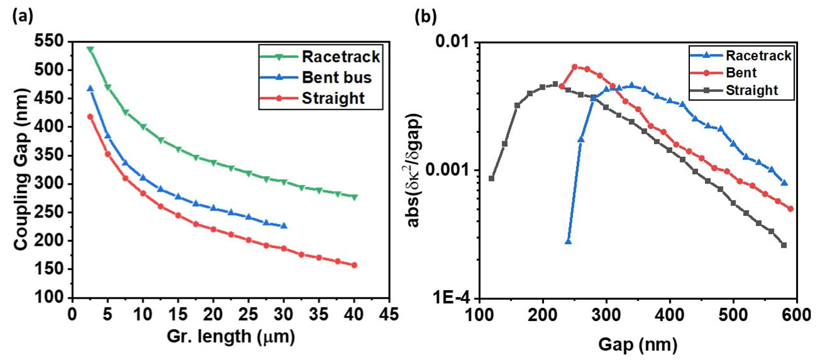
Figure 7a compares the required coupling gap to reach critical coupling for three different bus–ring configurations—straight, bent, and racetrack—as a function of graphene length.
The results reveal that for any given graphene length, the racetrack configuration consistently requires a larger coupling gap to achieve the same
value, followed by the bent bus, while the straight bus yields the smallest required gap. This behavior is attributed to the mode overlap efficiency of each geometry: racetrack couplers, due to their extended interaction length and geometry-induced mode mismatch, require larger physical gaps to reach a specific coupling strength as illustrated in
Figure 5d. Complementary to this,
Figure 7b shows the sensitivity of the coupling efficiency (∂
/∂gap) for all three configurations. For all structures, a peak in sensitivity is observed at intermediate gap values, with racetrack designs showing a delayed peak due to their broader coupling region. This indicates that racetrack-coupled modulators can maintain high coupling efficiency even at increased gap values, offering enhanced design flexibility. As a result, such designs are able to maintain operation near the critical coupling point even in the presence of minor variations in the coupling gap, thereby improving overall device robustness without sacrificing modulation performance. The results presented here reinforce that each structure imposes a unique coupling profile, which in turn affects the required graphene length and achievable modulation contrast. Therefore, design optimization must be co-dependent on both the coupler layout and absorption characteristics, ensuring that the structure operation near the desired critical point has sufficient tolerance and efficiency. To comprehensively assess the modulation behavior at a fixed coupling gap of 300 nm across different bus configurations, transmission spectra were simulated for straight, bent, and racetrack-coupled micro-ring modulators, with each design tuned to operate near its critical coupling point. For each configuration, a range of gate-tunable graphene chemical potentials μ was applied—from 0 to 0.57 eV—to modulate absorption and hence the effective loss
α. The performance was benchmarked using key figures of merit: modulation depth (MD), extinction ratio (ER), insertion loss (IL), resonance wavelength shifting between graphene on and off Δλ, full width at half maximum (FWHM), and the photon lifetime limited 3 dB bandwidth (BW), which is defined as follows:
where c is the light speed,
is the resonance wavelength, and Q is the loaded quality factor of the graphene ring modulators. Using these values, the overall figure of merit (FOM) is defined as follows:
In the straight bus configuration (
Figure 8a,b), the graphene length was set to 7.5 µm for optimal critical coupling. Sweeping μ resulted in a maximum modulation depth of 18.09 dB and a narrow FWHM of 0.22 nm, with a corresponding BW of 38.66 GHz. The resonance wavelength shifted by ~0.020 nm with gating, and the average insertion loss (
) between the ON and OFF states was ~19 dB. A 15% increase in graphene length caused a red shift in resonance (~2.85 nm), and slightly reduced ER, though the bandwidth remained comparable. In the bent bus configuration (
Figure 8c,d), a longer graphene length of 10 µm was needed due to lower the coupling efficiency. The transmission spectrum showed broader FWHM (0.32 nm), larger BW (~65.89 GHz), and MD of 16.53 dB, with
~19.7 dB. Upon a 15% length increase, a wavelength red shift of ~0.25 nm occurred, and modulation performance remained largely stable. The FOM stayed consistent around 1.5 × 10⁹, slightly higher than the straight bus design. In the racetrack configuration (
Figure 8e,f), a graphene length of 30 µm achieved deep modulation with MD ~28.50 dB,
~26 dB, and a wide BW of 162.09 GHz. The variation in photon life limited bandwidth coming from the quality factor of the resonator and at different chemical potentials of the graphene is plotted in
Figure 9. Thus, enhanced bandwidth is primarily attributed to the reduced quality factor of the resonator, owing to larger graphene section as shown in
Figure 9.
Notably, introducing a 15% increase in graphene length in the racetrack structure (
Figure 8f) did not degrade the modulation depth or significantly shift the resonance wavelength, demonstrating robustness in performance, which was observed. However, to maintain optimal contrast for slightly deviated graphene length, a different chemical potential μ had to be selected for the ON state. This observation suggests that minor adjustments in gate voltage can compensate for physical variations in the graphene length, effectively preserving key modulation parameters such as MD, bandwidth, and resonance alignment. Thus, racetrack geometries not only enable high-performance modulation but also present the potential for voltage-level compensation strategies to mitigate performance degradation arising from variations in physical parameters such as coupling gap and graphene length. Moreover, the FOM is overall larger in racetrack than the straight and bent bus designs and further improves from 5.25 × 10⁹ to 7.37 × 10⁹ when the graphene length is changed, reflecting unchanged performance with even a 15 percent deviation in graphene length.
Since no direct study on bus geometry’s dependence on critical coupling gaps and modulation depth has been reported to date, the performance of the proposed racetrack modulator can still be compared with previously published works. For instance, Lee et al. [
34] demonstrated a graphene–silicon nitride electro-absorption ring modulator with a 180 nm coupling gap where a modulation depth of 7 dB at 9 V was achieved. By contrast, the racetrack design proposed here, which features a much wider 300 nm coupling gap, achieves an approximately four times higher modulation depth (28 dB over 10 V). Furthermore, experimental data from Phare et al. [
19] indicate a 15 dB modulation depth at a 10 V drive voltage. In contrast, the device presented in this work demonstrates 30 dB modulation depth under the same drive conditions, effectively doubling Phare et al.’s result. In another study by Faneca et al. [
35], the modulator reached a modulation depth of 16.5 dB at a 10 V swing, with the values two times lower than the racetrack modulator.
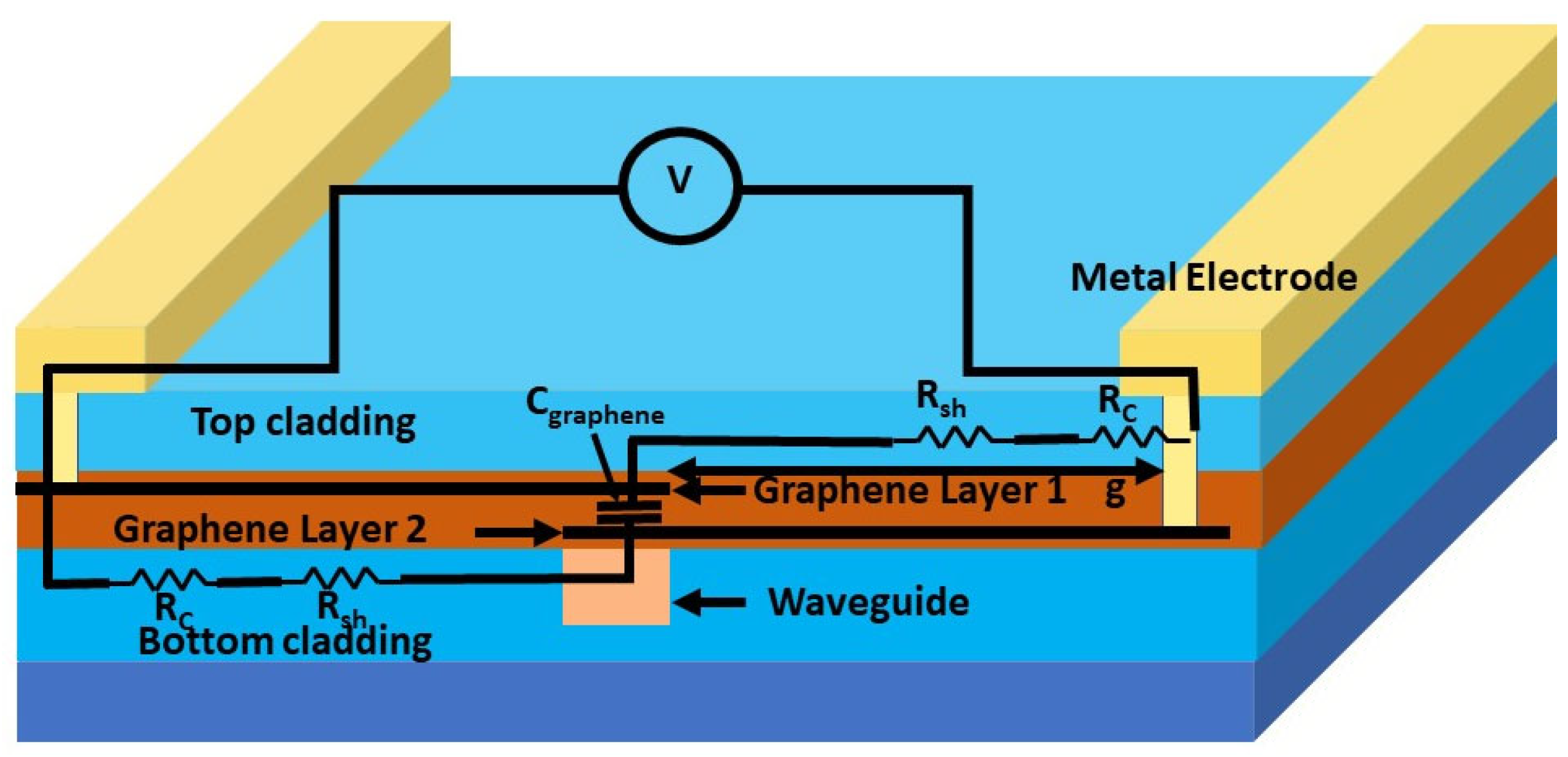
As voltage-dependent performance has been evaluated, the following key parameter has to be considered: the bandwidth of the modulator.
Figure 10 shows the cross-sectional view of the device overlaid with the various resistances and the capacitance used to estimate the bandwidth of the device. To fabricate the via contact to graphene, standard pilot-line-compatible processes involve etching vias through the dielectric using controlled wet or dry methods (e.g., hot phosphoric acid or low-power plasma), followed by metal deposition (e.g., Ni/TiN/W) to form low-resistance edge or surface contacts, as demonstrated in integrated graphene devices [
36,
37]. The RC time-limited 3 dB bandwidth of such configuration is obtained as follows:
where
is the contact resistance,
is the sheet resistance of the graphene, g = 0.8 μm is the distance between the metal electrode and the graphene capacitor, w is the graphene capacitor, d is the spacer layer thickness, and l = 30 μm is the graphene length. Nevertheless, it is clear from Equation (12) that the contribution of l coming from the sheet resistance and the graphene capacitance cancels out. Therefore, Equation (12) is reduced to the following:
Equation (13) is plotted in
Figure 11 as a function of contact resistance. With the parameters values
and
an RC-limited bandwidth of 91 GHz can be achieved. The bandwidth of the measured device remains below the photon-limited bandwidth of over 200 GHz for 30 µm long graphene (
Figure 9), indicating that the RC bandwidth currently imposes the main limitation. Nonetheless, there is potential for further improvement in the overall RC modulation bandwidth by enhancing graphene quality and reducing metal contact resistance.
Table 1 summarizes a comprehensive comparison of key performance metrics for dual-layer graphene ring modulators reported in the literature. To the best of our knowledge, no prior work has demonstrated a dual-layer graphene-based modulator with a bent bus coupling configuration operating on the principle of electro-absorption modulation.
Notably, the proposed racetrack modulator in this work achieves 90 GHz of overall modulation bandwidth—1.5 times the 60 GHz (without 50 Ω load resistor) demonstrated by Phare et al. [
19] and four times higher than the 14.7 GHz reported by Lee et al. [
34], both of which are experimental studies. This represents a significant improvement, even when compared to theoretical simulations: the racetrack modulator designed here surpasses the 42.6 GHz bandwidth of the straight bus modulator modeled by Neves et al. [
38] by 18 GHz. Furthermore, while Neves et al. employed a 25% graphene coverage and a 205 nm coupling gap, the racetrack graphene modulator presented here achieves 28 dB of modulation depth with 12% graphene coverage and a wider 300 nm coupling gap yet still delivers a theoretical bandwidth of 90 GHz. This choice of 300 nm gap was intentionally made to ensure a consistent baseline for performance comparison with the straight and bent bus modulator designs, all evaluated under similar coupling sensitivity conditions. Notably, even at this relatively large gap, the racetrack configuration maintains a high coupling efficiency of approximately 0.78—substantially higher than what is typically achievable with a bent or straight bus configuration at the same gap. Moreover, due to the extended interaction length inherent in the racetrack geometry, the coupling efficiency remains sufficiently strong even at gaps as large as 400 nm, offering significant flexibility in fabrication without compromising performance. Therefore, even with the reduced coverage/area of the graphene, the device can still achieve modulation depths as high as 18 dB, highlighting the strength of the racetrack-based design and its potential for further optimization in high-speed and high-modulation-efficiency photonic devices.


 ,
, 


