
Self-Calibrating TSEP for Junction Temperature and RUL Prediction in GaN HEMTs
 , , ,
, , , 
Abstract
1. Introduction
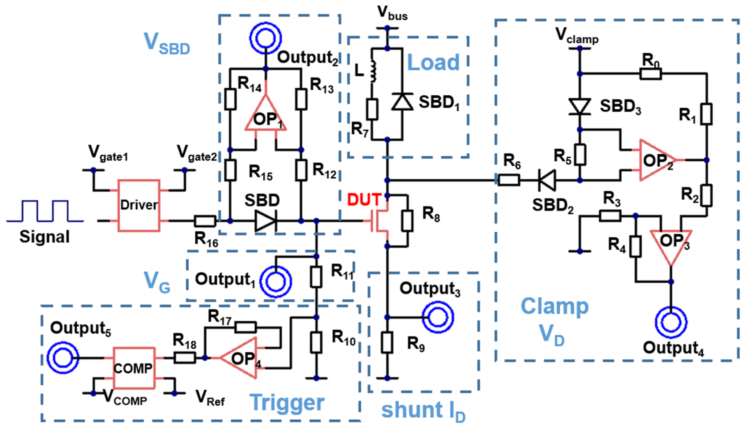
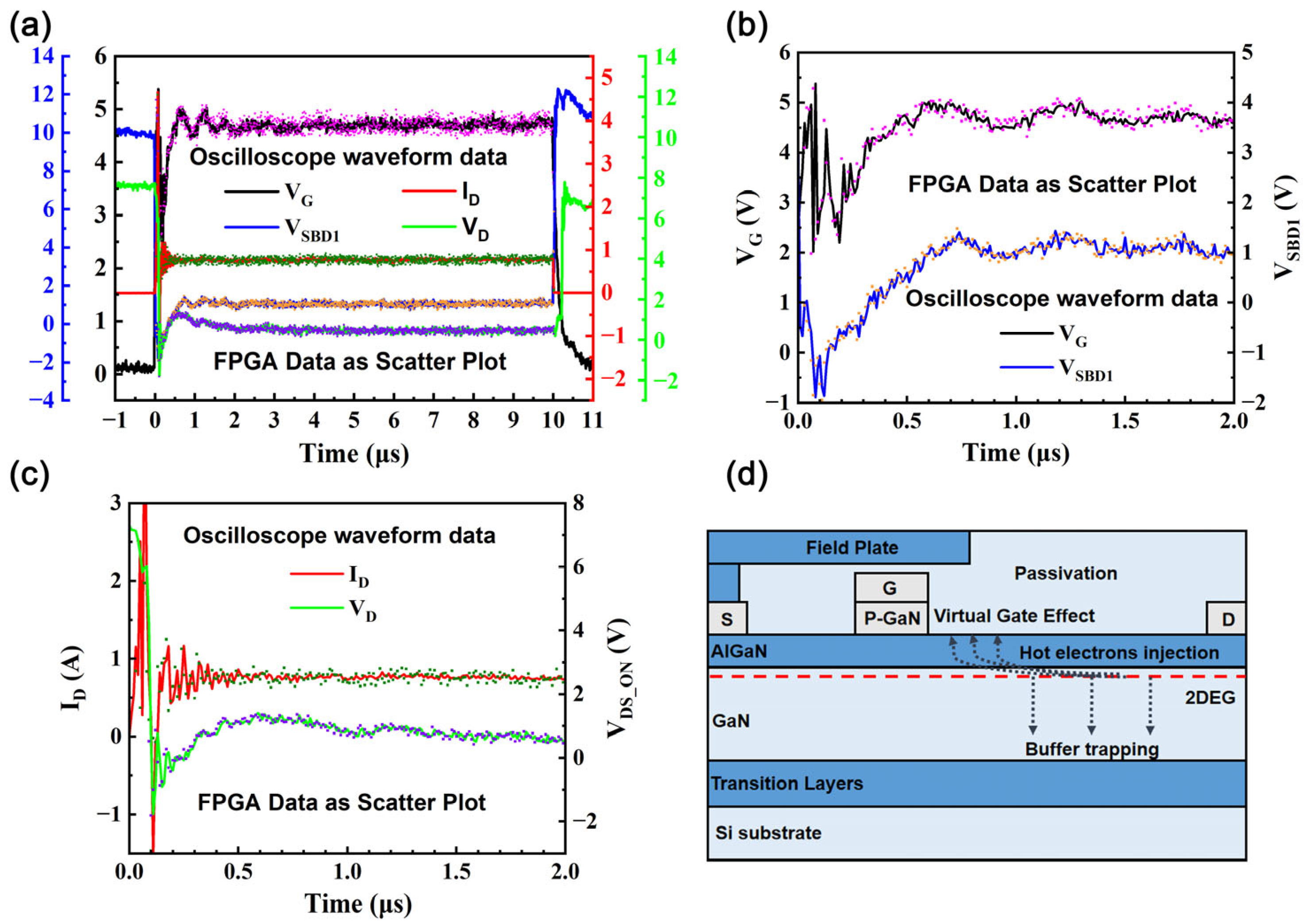
2. Experiment Setup
- A.
- Design of the Multiple-Pulse Tester board
- B.
- Extraction of RDS_ON and IG
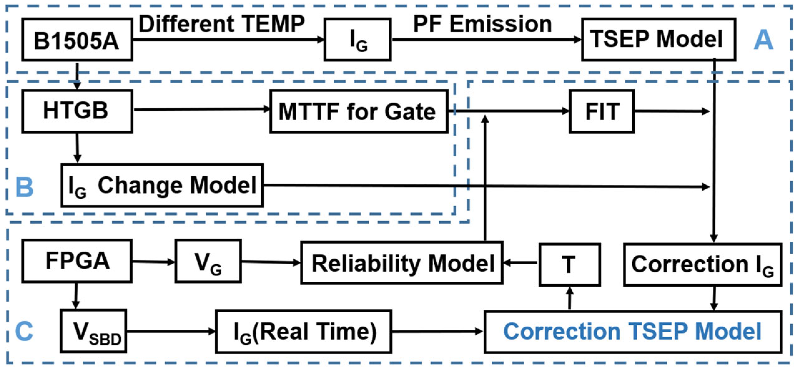
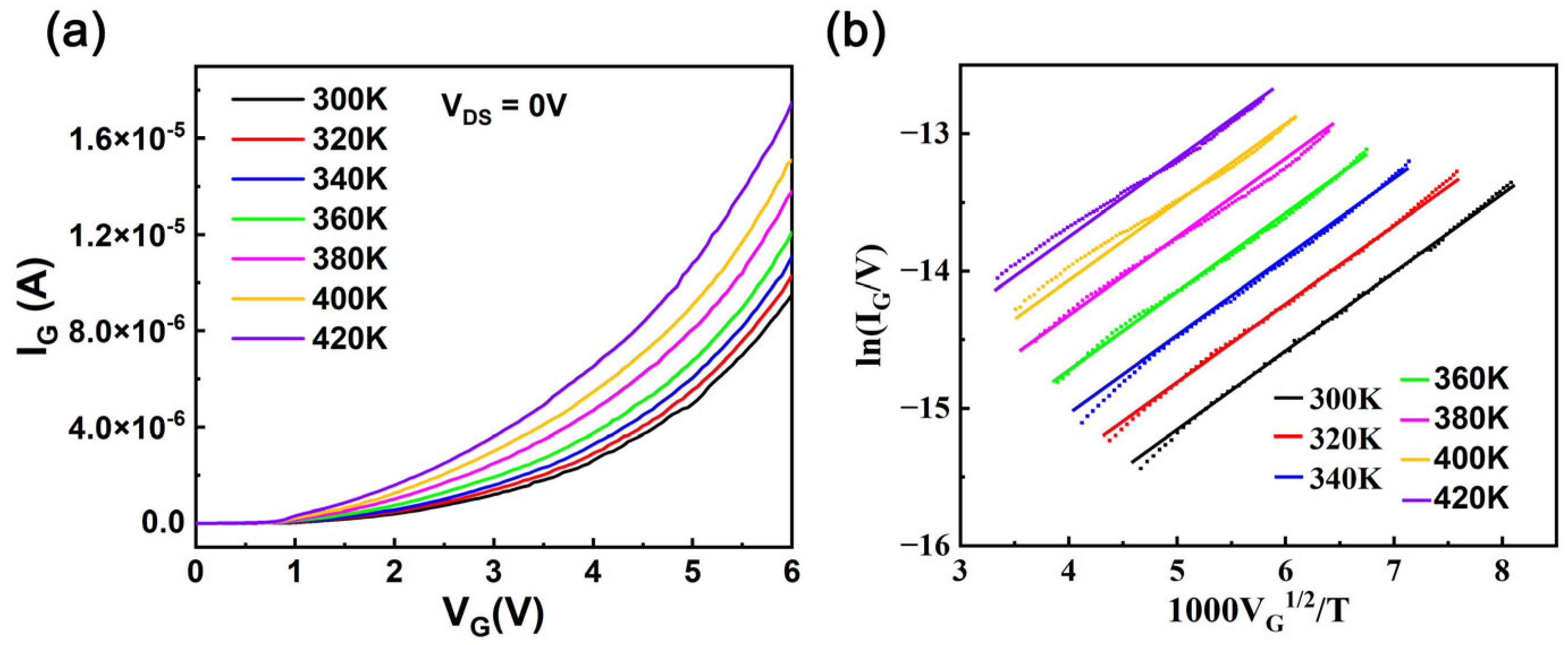
3. Modeling and Calibration of the Temperature-Sensitive Parameter (IG) for HEMTs
- A.
- Operating Principle and Modeling of TSEPs for HEMTs
- B.
- Modeling of IG Variations and Lifetime Assessment of HEMT
- C.
- TSEP Model Calibration Based on the Gate FIT and Aging-Dependent IG Change Model
- Utilize Equation (7) to calculate the MTTF required in (11) for the specific operating conditions.
- Utilize Equation (11) to calculate the equivalent stress time required in (4).
- Utilize Equation (4) to calculate the origin IG.
- Utilize Equation (3) to calculate the effect of junction temperature on IG.
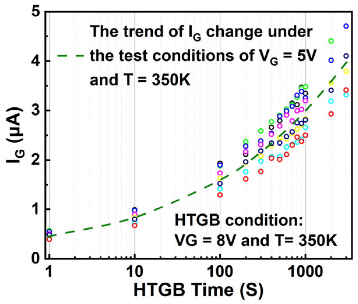
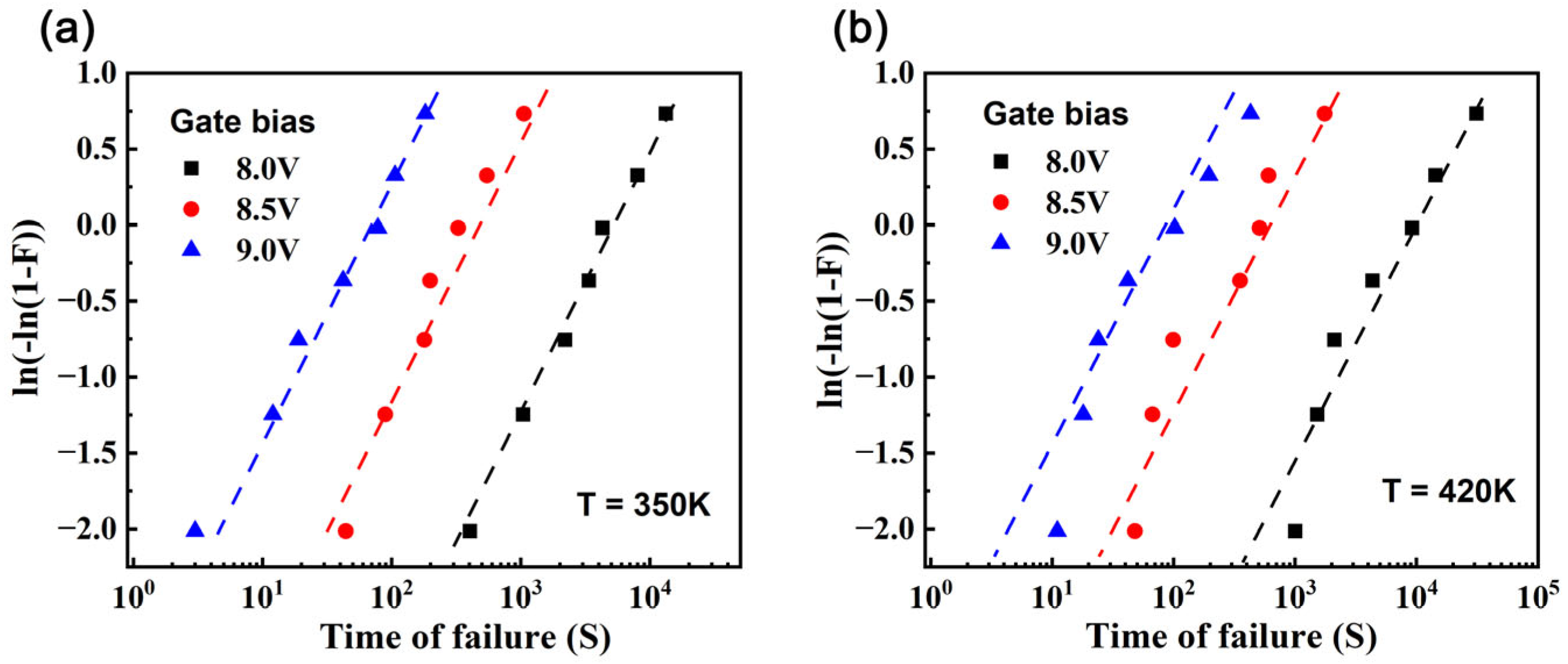
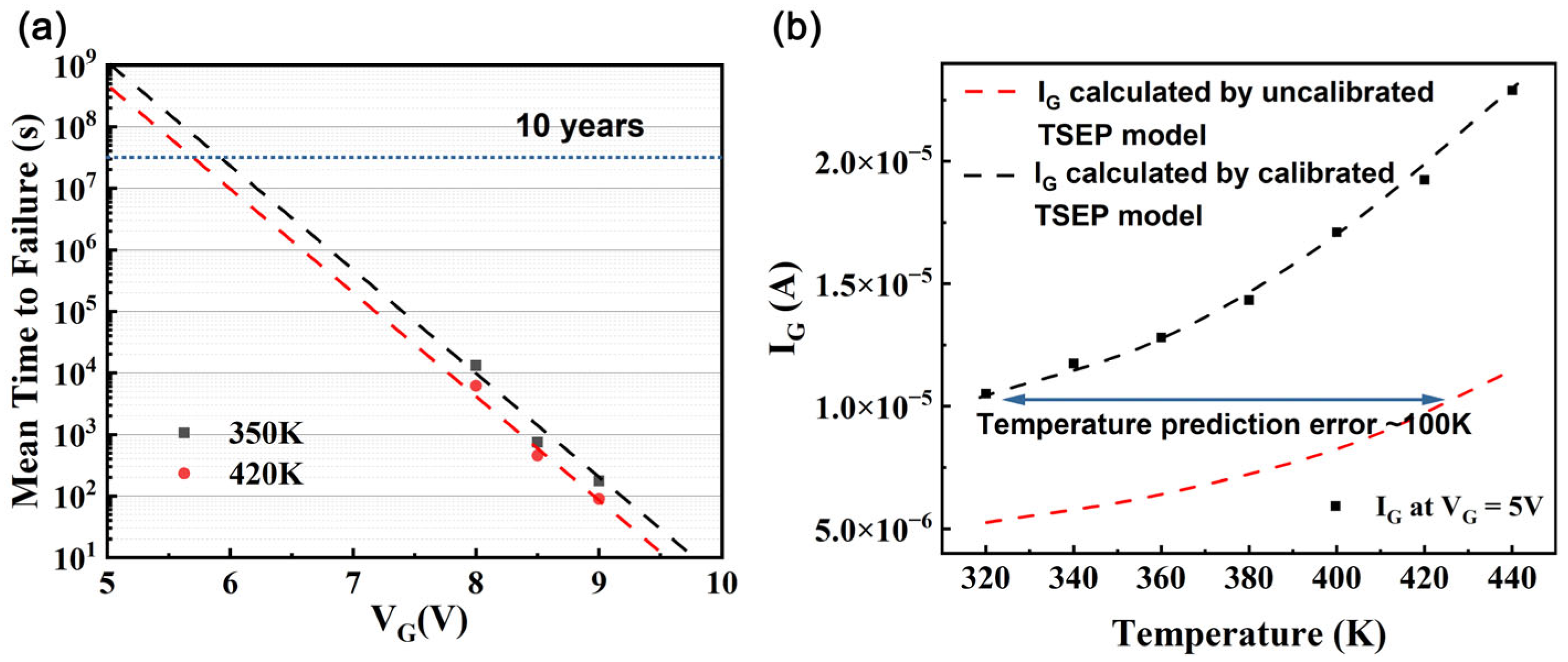
4. Long-Term Test Results and RUL Prediction
5. Conclusions
Author Contributions
Funding
Data Availability Statement
Acknowledgments
Conflicts of Interest
References
- Buffolo, M.; Favero, D.; Marcuzzi, A.; De Santi, C.; Meneghesso, G.; Zanoni, E.; Meneghini, M. Review and Outlook on GaN and SiC Power Devices: Industrial State-of-the-Art, Applications, and Perspectives. IEEE Trans. Electron Devices 2024, 71, 1344–1355. [Google Scholar] [CrossRef]
- Zhang, Y.; Udrea, F.; Wang, H. Multidimensional Device Architectures for Efficient Power Electronics. Nat. Electron. 2022, 5, 723–734. [Google Scholar] [CrossRef]
- Amano, H.; Baines, Y.; Beam, E.; Borga, M.; Bouchet, T.; Chalker, P.R.; Charles, M.; Chen, K.J.; Chowdhury, N.; Chu, R.; et al. The 2018 GaN power electronics roadmap. J. Phys. D Appl. Phys. 2018, 51, 163001. [Google Scholar] [CrossRef]
- Jain, S.K.; Low, M.X.; Vashishtha, P.; Nirantar, S.; Zhu, L.; Ton-That, C.; Ahmed, T.; Sriram, S.; Walia, S.; Gupta, G.; et al. Influence of Temperature on Photodetection Properties of Honeycomb-like GaN Nanostructures. Adv. Mater. Interfaces 2021, 8, 2100593. [Google Scholar] [CrossRef]
- Vashishtha, P.; Verma, A.K.; Walia, S.; Gupta, G. A Solar-Blind Ultraviolet Photodetector with Self-Biasing Capability Controlled by Surface Potential based on GaN Hexagonal Nano-Spikes. Mater. Lett. 2024, 368, 136708. [Google Scholar] [CrossRef]
- Vashishtha, P.; Jain, S.K.; Prajapat, P.; Verma, A.K.; Aggarwal, N.; Murdoch, B.J.; Walia, S.; Gupta, G. A Self-Driven Bidirectional Photocurrent Photodetector for Optically Controlled Logic Gates Utilizes a GaN-Nanowall Network. ACS Appl. Opt. Mater. 2024, 2, 1353–1359. [Google Scholar] [CrossRef]
- Bahl, S.R.; Ruiz, J.; Zehnder, D.; Faili, F. Application Reliability Validation of GaN Power Devices. In Proceedings of the IEEE International Electron Devices Meeting, San Francisco, CA, USA, 10–14 December 2016. [Google Scholar]
- Oh, H.; Han, B.; McCluskey, P.; Han, C.; Youn, B.D. Physics-of-Failure, Condition Monitoring, and Prognostics of Insulated Gate Bipolar Transistor Modules: A Review. IEEE Trans. Power Electron 2015, 30, 2413–2426. [Google Scholar] [CrossRef]
- Kozak, J.P.; Zhang, R.; Ngo, K.D.T.; Hudgins, J.L.; Vallin, O.; Sandvik, E.; Chow, T.P.; Eden, J.G. Stability, Reliability, and Robustness of GaN Power Devices: A Review. IEEE Trans. Power Electron 2023, 38, 8447–8464. [Google Scholar] [CrossRef]
- Meneghini, M.; Santi, C.D.; Abid, I.; Buffolo, M.; Cioni, M.; Khadar, R.A.; Nela, L.; Zagni, N.; Chini, A.; Medjdoub, F.; et al. GaN-Based Power Devices: Physics, Reliability, and Perspectives. J. Appl. Phys. 2021, 130, 181101. [Google Scholar] [CrossRef]
- Lin, M.; Bahl, S.R.; Zehnder, D. New Circuit Topology for System-Level Reliability of GaN. In Proceedings of the International Symposium on Power Semiconductor Devices and ICs, Shanghai, China, 19–23 May 2019. [Google Scholar]
- Yin, S.; Li, J.; Hua, M.; Tang, G.; Zhang, J.C.; Chen, K.J. Evaluation of Reliability and Lifetime of 650-V GaN-on-Si Power Devices Fabricated on 200-mm CMOS-Compatible Process Platform for High-Density Power Converter Application. In Proceedings of the 34th International Symposium on Power Semiconductor Devices and ICs (ISPSD), Vancouver, BC, Canada, 22–26 May 2022. [Google Scholar]
- Bahl, S.R.; Baltazar, F.; Xie, Y. A Generalized Approach to Determine the Switching Lifetime of a GaN FET. In Proceedings of the IEEE International Reliability Physics Symposium, Dallas, TX, USA, 28 April–30 May 2020. [Google Scholar]
- Huang, Y.; Tang, G.; Zhang, J.C.; Chen, K.J. Investigation of Saturated RON on GaN Power HEMTs by a Re-Configurable Continuous Switching Platform. IEEE Trans. Power Electron 2024, 71, 9876–9884. [Google Scholar] [CrossRef]
- Li, S.; Yang, S.; Han, S.; Sheng, K. Investigation of Temperature-Dependent Dynamic RON of GaN HEMT with Hybrid-Drain under Hard and Soft Switching. In Proceedings of the International Symposium on Power Semiconductor Devices and ICs, Vienna, Austria, 13–18 September 2020. [Google Scholar]
- Lu, X. Investigation and Comparison of Temperature-Sensitive Electrical Parameters of SiC MOSFET at Extremely High Temperatures. IEEE Trans. Power Electron 2023, 38, 9987–9995. [Google Scholar] [CrossRef]
- Yu, H.; Jiang, X.; Chen, J.; Wang, J.; Shen, Z.J. A Novel Real-Time Junction Temperature Monitoring Circuit for SiC MOSFET. In Proceedings of the IEEE Applied Power Electronics Conference and Exposition, New Orleans, LA, USA, 15–19 March 2020. [Google Scholar]
- Sun, P.; Guo, Y.; Wu, T.; Zhao, Z.; Lai, P.; Chen, Z.; Qi, L.; Cui, X. An Online Junction Temperature Monitoring Correction Method for SiC MOSFETs at Different Parasitic Parameters. IEEE J. Emerg. Sel. Top. Power Electron 2022, 10, 5007–5018. [Google Scholar] [CrossRef]
- Melkonyan, A.; Schulz, M. Advanced Gate Drive Unit for Junction Temperature Monitoring and Dynamic Current Balancing of GaN Transistors Operating in Parallel. In Proceedings of the IEEE Applied Power Electronics Conference and Exposition, New Orleans, LA, USA, 15–19 March 2020. [Google Scholar]
- Borghese, A.; Riccio, M.; Maresca, L.; Breglio, G.; Irace, A. Gate Driver for p-GaN HEMTs with Real-Time Monitoring Capability of Channel Temperature. In Proceedings of the 33rd International Symposium on Power Semiconductor Devices and ICs (ISPSD), Nagoya, Japan, 30 May–3 June 2021. [Google Scholar]
- Goller, M.; Franke, J.; Lentzsch, T.; Lutz, J.; Basler, T.; Mouhoubi, S. Determination of the Junction Temperature Under Load Current in GaN Power Devices with Schottky Gate Leakage Current as TSEP. In Proceedings of the 36th International Symposium on Power Semiconductor Devices and ICs (ISPSD), Tokyo, Japan, 2–6 June 2024. [Google Scholar]
- He, J.; Wei, J.; Chen, K.J. Frequency- and Temperature-Dependent Gate Reliability of Schottky-Type p-GaN Gate HEMTs. IEEE Trans. Electron Devices 2019, 66, 3456–3461. [Google Scholar] [CrossRef]
- Tallarico, A.N.; Stoffels, S.; Magnani, A.; Posthuma, N.; Saggio, M.; Decoutere, S.; Marcon, D. P-GaN Gate HEMTs: A Solution to Improve the High-Temperature Gate Lifetime. IEEE Electron Device Lett. 2024, 45, 1630–1633. [Google Scholar] [CrossRef]
- Chihani, O.; Borga, M.; Decoutere, S.; Meneghesso, G.; Meneghini, M. Temperature and Voltage Effects on HTRB and HTGB Stresses for AlGaN/GaN HEMTs. In Proceedings of the International Symposium on Power Semiconductor Devices and ICs, Chicago, IL, USA, 13–17 May 2018. [Google Scholar]
- JEP122H; JEDEC Standard. Failure Mechanisms and Models for Semiconductor Devices. JEDEC Solid State Technology Association: Arlington, VA, USA, 2016.
- Khandelwal, S.; Chauhan, Y.S.; Fjeldly, T.A.; Ghosh, S.; Pampori, A.; Mahajan, A.; Dutta, R.; Ahsan, S.A.; Gupta, S.; Sharan, S.; et al. ASM GaN: Industry Standard Model for GaN RF and Power Devices—Part 1: DC, CV, and RF Model. IEEE Trans. Electron Devices 2019, 66, 80–86. [Google Scholar] [CrossRef]
- Stockman, A.; Canato, E.; Tajalli, A.; Meneghini, M.; Meneghesso, G.; Moens, P.; Zanoni, E.; Bakeroot, B. Temperature Dependent Substrate Trapping in AlGaN/GaN Power Devices and the Impact on Dynamic Ron. In Proceedings of the 47th European Solid-State Device Research Conference, Leuven, Belgium, 11–14 September 2017. [Google Scholar]
- Modolo, N.; De Santi, C.; Minetto, A.; Sayadi, L.; Sicre, S.; Prechtl, G.; Meneghesso, G.; Zanoni, E.; Meneghini, M. A Physics-Based Approach to Model Hot-Electron Trapping Kinetics in p-GaN HEMTs. IEEE Electron Device Lett. 2021, 42, 673–676. [Google Scholar] [CrossRef]
- Hu, C. Lucky-Electron Model of Channel Hot Electron Emission. In Proceedings of the International Electron Devices Meeting, Washington, DC, USA, 3–5 December 1979. [Google Scholar]
- Xu, N.; Hao, R.; Ou, F.; Chen, P.; Zhang, W.; Zhang, B.; Chen, K.J. Gate Leakage Mechanisms in Normally Off p-GaN/AlGaN/GaN High Electron Mobility Transistors. Appl. Phys. Lett. 2018, 113, 152104. [Google Scholar] [CrossRef]
- Yeargan, J.R.; Taylor, H.L. The Poole–Frenkel Effect with Compensation Present. J. Appl. Phys. 1968, 39, 5600–5604. [Google Scholar] [CrossRef]
- Tang, S.-W.; Li, K.; Wei, J.; Yang, S.; Chen, K.J. Using Gate Leakage Conduction to Understand Positive Gate Bias Induced Threshold Voltage Shift in p-GaN Gate HEMTs. IEEE Trans. Electron Devices 2023, 70, 449–453. [Google Scholar] [CrossRef]
- He, J.; Wei, J.; Li, Y.; Zheng, Z.; Yang, S.; Huang, B.; Chen, K.J. Characterization and Analysis of Low-Temperature Time-to-Failure Behavior in Forward-Biased Schottky-Type p-GaN Gate HEMTs. Appl. Phys. Lett. 2020, 116, 223502. [Google Scholar] [CrossRef]
- Jiang, Z.; Wang, X.; Chen, J.; Zhao, J.; Wang, H.; Chen, H.; Ma, J.; Hua, M. Roles of Hole Trap on Gate Leakage of p-GaN HEMTs at Cryogenic Temperatures. IEEE Electron Device Lett. 2023, 44, 1602–1605. [Google Scholar] [CrossRef]
- Zhang, R. In-situ RDS(ON) Characterization and Lifetime Projection of GaN HEMTs under Repetitive Overvoltage Switching. IEEE Trans. Power Electron. 2023, 38, 10589–10594. [Google Scholar] [CrossRef]
- Vici, A. A Multi-Energy Level Agnostic Approach for Defect Generation during TDDB Stress. Solid-State Electron. 2022, 193, 108298. [Google Scholar] [CrossRef]
- Gajare, S.; Francis, D.; Faili, F.; Ejeckam, F.; Twitchen, D.; Babic, D. GaN Reliability and Lifetime Projections: Phase 16; EPC Corp. Reliability Report; EPC: El Segundo, CA, USA, February 2024. [Google Scholar]
- Zhang, S.; Espinoza, A.; Garcia, R.; Gao, H.; Gajare, S.; Gorgerino, A. Duty Cycle-Based Repetitive Transient Overvoltage Specification for GaN HEMTs. In Proceedings of the 36th International Symposium on Power Semiconductor Devices and ICs (ISPSD), Tokyo, Japan, 2–6 June 2024. [Google Scholar]
- JESD85A; JEDEC Standard, “Method for Calculating Failure Rates in Units of FITS”. JEDEC Solid State Technology Association: Arlington, VA, USA, 2014.
- Li, S.; Sheng, K.; Yang, S. Temperature-Dependent Dynamic RON of GaN E-HEMTs: The Impact of p-GaN Drain. IEEE Trans. Power Electron. 2023, 70, 6789–6795. [Google Scholar] [CrossRef]
- Yang, J.; Li, Y.; Wei, J.; Yang, S.; Chen, K.J. Suppression of Hot-Electron-Induced Dynamic RON Degradation in p-GaN Gate HEMT Using Active Passivation and Virtual Body. In Proceedings of the International Symposium on Power Semiconductor Devices and ICs, Tokyo, Japan, 2–6 June 2024. [Google Scholar]
- Pozo, A.; Zhang, S.; Stecklein, G.; Garcia, R.; Glaser, J.; Tang, Z.; Strittmatter, R. EPC eGaN® Device Reliability Testing: Phase 12, Reliability Report Phase 12.pdf. Copyright 2021. Available online: https://epc-co.com/epc/design-support/gan-fet-reliability (accessed on 11 July 2025).


| Component | Specification | Role |
|---|---|---|
| Gate Driver IC | LMG1025-Q1 | Reduces gate noise. |
| Small Signal Schottky Diode | 1N6263 | Monitors IG via VSBD. |
| Current Shunt Resistor | SSDN-414-10, 0.1Ω | Measures IDS_ON current. |
| Operational Amplifiers | LM6172IMX | High-speed test. |
Disclaimer/Publisher’s Note: The statements, opinions and data contained in all publications are solely those of the individual author(s) and contributor(s) and not of MDPI and/or the editor(s). MDPI and/or the editor(s) disclaim responsibility for any injury to people or property resulting from any ideas, methods, instructions or products referred to in the content. |
© 2025 by the authors. Licensee MDPI, Basel, Switzerland. This article is an open access article distributed under the terms and conditions of the Creative Commons Attribution (CC BY) license (https://creativecommons.org/licenses/by/4.0/).
Share and Cite
Cui, Y.; Gan, Y.; Wen, K.; Jiang, Y.; Chen, C.; Wang, Q.; Yu, H. Self-Calibrating TSEP for Junction Temperature and RUL Prediction in GaN HEMTs. Nanomaterials 2025, 15, 1102. https://doi.org/10.3390/nano15141102
Cui Y, Gan Y, Wen K, Jiang Y, Chen C, Wang Q, Yu H. Self-Calibrating TSEP for Junction Temperature and RUL Prediction in GaN HEMTs. Nanomaterials. 2025; 15(14):1102. https://doi.org/10.3390/nano15141102
Chicago/Turabian StyleCui, Yifan, Yutian Gan, Kangyao Wen, Yang Jiang, Chunzhang Chen, Qing Wang, and Hongyu Yu. 2025. "Self-Calibrating TSEP for Junction Temperature and RUL Prediction in GaN HEMTs" Nanomaterials 15, no. 14: 1102. https://doi.org/10.3390/nano15141102
APA StyleCui, Y., Gan, Y., Wen, K., Jiang, Y., Chen, C., Wang, Q., & Yu, H. (2025). Self-Calibrating TSEP for Junction Temperature and RUL Prediction in GaN HEMTs. Nanomaterials, 15(14), 1102. https://doi.org/10.3390/nano15141102