
High-Performance GaN-Based Green Flip-Chip Mini-LED with Lattice-Compatible AlN Passivation Layer

Abstract

1. Introduction
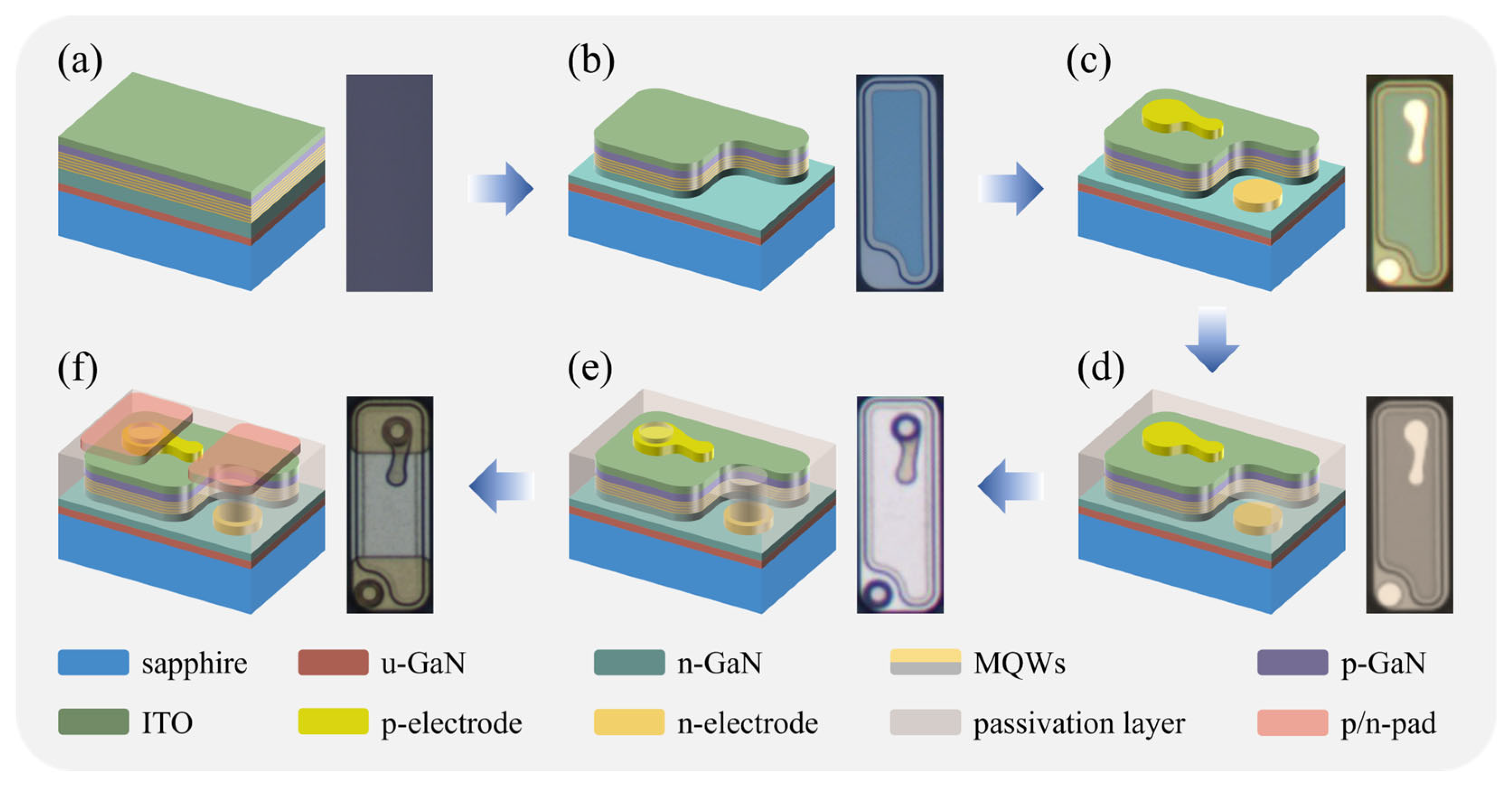
2. Experimental
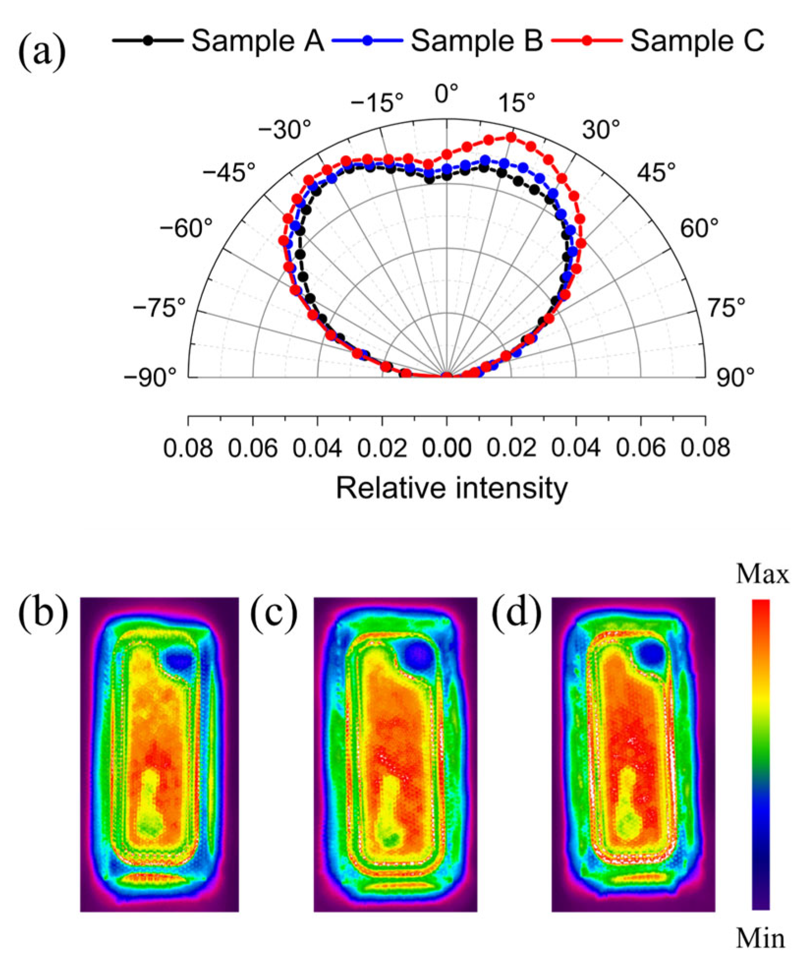
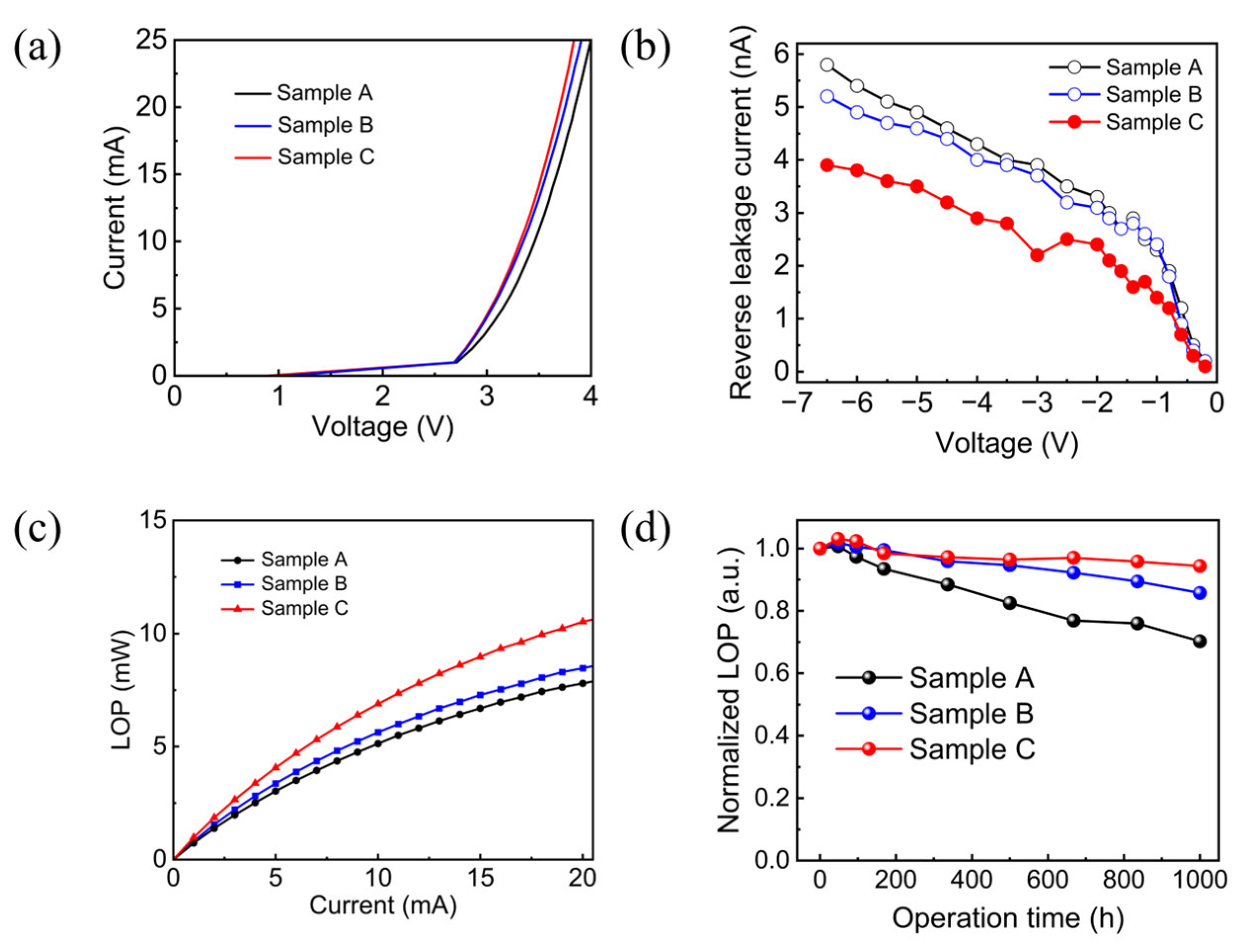
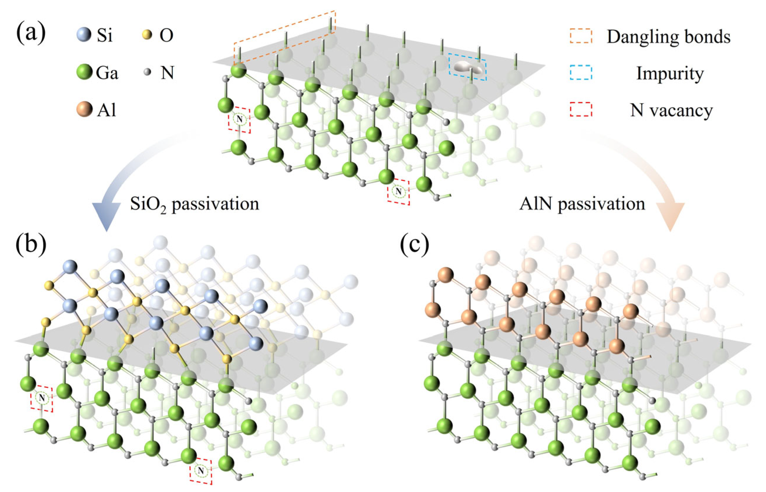
3. Results and Discussion
4. Conclusions
Author Contributions
Funding
Data Availability Statement
Conflicts of Interest
References
- Yang, G.; Chang, J.; Zhao, J.; Tong, Y.; Xie, F.; Wang, J.; Zhang, Q.; Huang, H.; Yan, D. Investigation of light output performance for gallium nitride-based light-emitting diodes grown on different shapes of patterned sapphire substrate. Mater. Sci. Semicond. Process. 2015, 33, 149–153. [Google Scholar] [CrossRef]
- Zhou, S.; Liu, X.; Yan, H.; Chen, Z.; Liu, Y.; Liu, S. Highly efficient GaN-based high-power flip-chip light-emitting diodes. Opt. Express 2019, 27, A669–A692. [Google Scholar] [CrossRef]
- Guo, W.; Chen, N.; Lu, H.; Su, C.; Lin, Y.; Chen, G.; Lu, Y.; Zheng, L.; Peng, Z.; Kuo, H.C. The Impact of Luminous Properties of Red, Green, and Blue Mini-LEDs on the Color Gamut. IEEE Trans. Electron. Devices 2019, 66, 2263–2268. [Google Scholar] [CrossRef]
- Fan, B.; Zhao, X.; Zhang, J.; Sun, Y.; Yang, H.; Guo, L.J.; Zhou, S. Monolithically Integrating Ⅲ-Nitride Quantum Structure for Full-Spectrum White LED via Bandgap Engineering Heteroepitaxial Growth. Laser Photonics Rev. 2023, 17, 2200455. [Google Scholar] [CrossRef]
- Shi, L.; Cui, S.; Zhang, Z.; Jiang, J.; Sun, Y.; Liu, S.; Zhou, S. Toward Wide-Angle Ⅲ-Nitride Miniaturized LEDs: Device Engineering and Photon Extraction Strategy. Laser Photonics Rev. 2025, 2401723. [Google Scholar] [CrossRef]
- Touré, A.; Halidou, I.; Benzarti, Z.; Fouzri, A.; Bchetnia, A.; El Jani, B. Characterization of low Al content AlXGa1-XN epitaxial films grown by atmospheric-pressure MOVPE. Phys. Status Solidi A 2012, 209, 977–983. [Google Scholar] [CrossRef]
- Olivier, F.; Daami, A.; Licitra, C.; Templier, F. Shockley-Read-Hall and Auger non-radiative recombination in GaN based LEDs: A size effect study. Appl. Phys. Lett. 2017, 111, 022104. [Google Scholar] [CrossRef]
- Ley, R.T.; Smith, J.M.; Wong, M.S.; Margalith, T.; Nakamura, S.; DenBaars, S.P.; Gordon, M.J. Revealing the importance of light extraction efficiency in InGaN/GaN microLEDs via chemical treatment and dielectric passivation. Appl. Phys. Lett. 2020, 116, 251104. [Google Scholar] [CrossRef]
- Dingemans, G.; Van de Sanden, M.C.M.; Kessels, W.M.M. Influence of the Deposition Temperature on the c-Si surface Passivation by Al2O3 Films Synthesized by ALD and PECVD. Electrochem. Solid-State Lett. 2009, 13, H76. [Google Scholar] [CrossRef]
- Cha, H.; Chang, H.S. Passivation performance improvement of ultrathin ALD-Al2O3 film by chemical oxidation. Vacuum 2018, 149, 180–184. [Google Scholar] [CrossRef]
- Tian, P.; McKendry, J.J.D.; Gong, Z.; Guilhabert, B.; Watson, I.M.; Gu, E.; Chen, Z.; Zhang, G.; Dawson, M.D. Size-dependent efficiency and efficiency droop of blue InGaN micro-light emitting diodes. Appl. Phys. Lett. 2012, 101, 231110. [Google Scholar] [CrossRef]
- Park, J.H.; Pristovsek, M.; Cai, W.; Cheong, H.; Tanaka, A.; Furusawa, Y.; Han, D.P.; Seong, T.Y.; Amano, H. Impact of Sidewall Conditions on Internal QuantumEfficiency and Light Extraction Efficiency of Micro-LEDs. Adv. Opt. Mater. 2023, 11, 2303128. [Google Scholar]
- Hang, S.; Zhang, M.; Zhang, Y.; Chu, C.; Zhang, Y.; Zheng, Q.; Li, Q.; Zhang, Z.H. Artificially formed resistive ITO/p-GaN junction to suppress the current spreading and decrease the surface recombination for GaN-based micro-light emitting diodes. Opt. Express 2021, 29, 31201–31211. [Google Scholar] [CrossRef]
- Zhuang, Z.; Iida, D.; Velazquez-Rizo, M.; Ohkawa, K. Ultra-small InGaN green micro-light-emitting diodes fabricated by selective passivation of p-GaN. Opt. Lett. 2021, 46, 5092–5095. [Google Scholar] [CrossRef]
- Hsu, Y.H.; Lin, X.D.; Lin, Y.H.; Wuu, D.S.; Horng, R.H. Performance comparison of flip-chip blue-light microLEDs with various passivation. Discov. Nano 2024, 19, 129. [Google Scholar] [CrossRef]
- Wong, M.S.; Lee, C.; Myers, D.J.; Hwang, D.; Kearns, J.A.; Li, T.; Speck, J.S.; Nakamura, S.; DenBaars, S.P. Size-independent peak efficiency of Ⅲ-nitride micro-light-emitting-diodes using chemical treatment and sidewall passivation. Appl. Phys. Express 2019, 12, 097004. [Google Scholar] [CrossRef]
- Lai, S.; Lin, W.; Chen, J.; Lu, T.; Liu, S.; Lin, Y.; Lu, Y.; Lin, Y.; Chen, Z.; Kuo, H.C.; et al. The impacts of sidewall passivation via atomic layer deposition on GaN-based flip-chip blue mini-LEDs. J. Phys. D Appl. Phys. 2022, 55, 374001. [Google Scholar] [CrossRef]
- Yeh, Y.W.; Lin, S.H.; Hsu, T.C.; Lai, S.; Lee, P.T.; Lien, S.Y.; Wuu, D.S.; Li, G.; Chen, Z.; Wu, T.; et al. Advanced Atomic Layer Deposition Technologies for Micro-LEDs and VCSELs. Nanoscale Res. Lett. 2021, 16, 164. [Google Scholar] [CrossRef]
- Huang Chen, S.W.; Shen, C.C.; Wu, T.; Liao, Z.Y.; Chen, L.F.; Zhou, J.R.; Lee, C.F.; Lin, C.H.; Lin, C.C.; Sher, C.W.; et al. Full-color monolithic hybrid quantum dot nanoring micro light-emitting diodes with improved efficiency using atomic layer deposition and nonradiative resonant energy transfer. Photonics Res. 2019, 7, 416–422. [Google Scholar] [CrossRef]
- Deng, Y.; Chen, J.; Li, S.; Huang, H.; Liu, Z.; Yan, Z.; Lai, S.; Zheng, L.; Yang, T.; Chen, Z.; et al. The impacts of SiO2 atomic-layer-deposited passivation layer thickness on GaN-based green micro-LEDs. Semicond. Sci. Technol. 2024, 39, 045004. [Google Scholar] [CrossRef]
- Wong, M.S.; Hwang, D.; Alhassan, A.I.; Lee, C.; Ley, R.; Nakamura, S.; DenBaars, S.P. High efficiency of Ⅲ-nitride micro-light-emitting diodes by sidewall passivation using atomic layer deposition. Opt. Express 2018, 26, 21324–21331. [Google Scholar] [CrossRef] [PubMed]
- Lee, D.H.; Lee, J.H.; Park, J.S.; Seong, T.Y.; Amano, H. Improving the Leakage Characteristics and Efficiency of GaN-based Micro-Light-Emitting Diode with Optimized Passivation. ECS J. Solid State Sci. Technol. 2020, 9, 055001. [Google Scholar] [CrossRef]
- Prechatavanich, N.; Wu, M.J.; Yee, C.K.; Sutheebanjerd, T.; Tseng, Y.T.; Yang, Y.C.; Lee, C.A.; Lin, K.H.; Wu, C.H. Sidewall defect suppression of 620 nm AlGaInP-based red µLED devices using HfO2 ALD passivation. Opt. Lett. 2025, 50, 313–316. [Google Scholar] [CrossRef]
- Chen, D.; Wang, Z.; Hu, F.C.; Shen, C.; Chi, N.; Liu, W.; Zhang, D.V.; Lu, H.L. Improved electro-optical and photoelectric performance of GaN-based micro-LEDs with an atomic layer deposited AlN passivation layer. Opt. Express 2021, 29, 36559–36566. [Google Scholar] [CrossRef]
- Zhou, S.; Liao, Z.; Sun, K.; Zhang, Z.; Qian, Y.; Liu, P.; Du, P.; Jiang, J.; Lv, Z.; Qi, S. High-Power AlGaN-Based Ultrathin Tunneling Junction Deep Ultraviolet Light-Emitting Diodes. Laser Photonics Rev. 2023, 18, 2300464. [Google Scholar] [CrossRef]
- Lee, T.Y.; Huang, Y.M.; Chiang, H.; Chao, C.L.; Hung, C.Y.; Kuo, W.H.; Fang, Y.H.; Chu, M.T.; Wu, C.I.; Lin, C.C.; et al. Increase in the efficiency of Ⅲ-nitride micro LEDs by atomic layer deposition. Opt. Express 2022, 30, 18552–18561. [Google Scholar] [CrossRef]
- Deng, Y.; Li, D.; Dai, Y.; Lin, Z.; Lin, Y.; Liu, Z.; Chen, X.; Kuo, H.C.; Chen, Z.; Lai, S.; et al. Competitive mechanism between light extraction efficiency and sidewall passivated effect in the green micro-LEDs with varied thickness of Al2O3 layer. Nanotechnology 2025, 36, 155201. [Google Scholar] [CrossRef]
- Liu, Z.; Cao, H.; Tang, X.; Liu, T.; Lu, Y.; Jiang, Z.; Xiao, N.; Li, X. Advanced technologies in InGaN micro-LED fabrication to mitigate the sidewall effect. Light: Sci. Appl. 2025, 14, 64. [Google Scholar] [CrossRef]
- Son, K.R.; Murugadoss, V.; Kim, K.H.; Kim, T.G. Investigation of sidewall passivation mechanism of InGaN-based blue microscale light-emitting diodes. Appl. Surf. Sci. 2022, 584, 152612. [Google Scholar] [CrossRef]
- Zhu, J.; Takahashi, T.; Ohori, D.; Endo, K.; Samukawa, S.; Shimizu, M.; Wang, X.L. Near-Complete Elimination of Size-Dependent Efficiency Decrease in GaN Micro-Light-Emitting Diodes. Phys. Status Solidi A 2019, 216, 1900380. [Google Scholar] [CrossRef]
- Yan, J.; Lu, W.; Li, J.; Huang, K.; Kang, J.; Zhang, R. Enhancing the Performance of Micro LEDs via Lightweight Atomic Charge-Matching Passivation. Adv. Opt. Mater. 2025, 2500796. [Google Scholar] [CrossRef]
- Kim, P.H.; Jeon, S.H.; Jang, J.H.; Han, S.; Kang, Y. Impact of Ga and N Vacancies at the GaN m-Plane on the Carrier Dynamics of Micro-Light-Emitting Diodes. Phys. Rev. Appl. 2023, 19, 014018. [Google Scholar] [CrossRef]
- Cao, D.; Cheng, X.; Xie, Y.H.; Zheng, L.; Wang, Z.; Yu, X.; Wang, J.; Shen, D.; Yu, Y. Effects of rapid thermal annealing on the properties of AlN films deposited by PEALD on AlGaN/GaN heterostructures. RSC Adv. 2015, 5, 37881–37886. [Google Scholar] [CrossRef]

Disclaimer/Publisher’s Note: The statements, opinions and data contained in all publications are solely those of the individual author(s) and contributor(s) and not of MDPI and/or the editor(s). MDPI and/or the editor(s) disclaim responsibility for any injury to people or property resulting from any ideas, methods, instructions or products referred to in the content. |
© 2025 by the authors. Licensee MDPI, Basel, Switzerland. This article is an open access article distributed under the terms and conditions of the Creative Commons Attribution (CC BY) license (https://creativecommons.org/licenses/by/4.0/).
Share and Cite
Song, J.; Shi, L.; Cui, S.; Meng, L.; Zhou, Q.; Jiang, J.; Jin, C.; Hu, J.; Wen, K.; Zhou, S. High-Performance GaN-Based Green Flip-Chip Mini-LED with Lattice-Compatible AlN Passivation Layer. Nanomaterials 2025, 15, 1048. https://doi.org/10.3390/nano15131048
Song J, Shi L, Cui S, Meng L, Zhou Q, Jiang J, Jin C, Hu J, Wen K, Zhou S. High-Performance GaN-Based Green Flip-Chip Mini-LED with Lattice-Compatible AlN Passivation Layer. Nanomaterials. 2025; 15(13):1048. https://doi.org/10.3390/nano15131048
Chicago/Turabian StyleSong, Jiahao, Lang Shi, Siyuan Cui, Lingyue Meng, Qianxi Zhou, Jingjing Jiang, Conglong Jin, Jiahui Hu, Kuosheng Wen, and Shengjun Zhou. 2025. "High-Performance GaN-Based Green Flip-Chip Mini-LED with Lattice-Compatible AlN Passivation Layer" Nanomaterials 15, no. 13: 1048. https://doi.org/10.3390/nano15131048
APA StyleSong, J., Shi, L., Cui, S., Meng, L., Zhou, Q., Jiang, J., Jin, C., Hu, J., Wen, K., & Zhou, S. (2025). High-Performance GaN-Based Green Flip-Chip Mini-LED with Lattice-Compatible AlN Passivation Layer. Nanomaterials, 15(13), 1048. https://doi.org/10.3390/nano15131048