
Excellent Room-Temperature NO2 Gas-Sensing Properties of TiO2-SnO2 Composite Thin Films Under Light Activation
 , , , , and
Abstract
1. Introduction
2. Materials and Methods
2.1. Chemicals and Substrates
2.2. Gas Sensor Design
2.3. Characterization of Thin Films
3. Results and Discussion
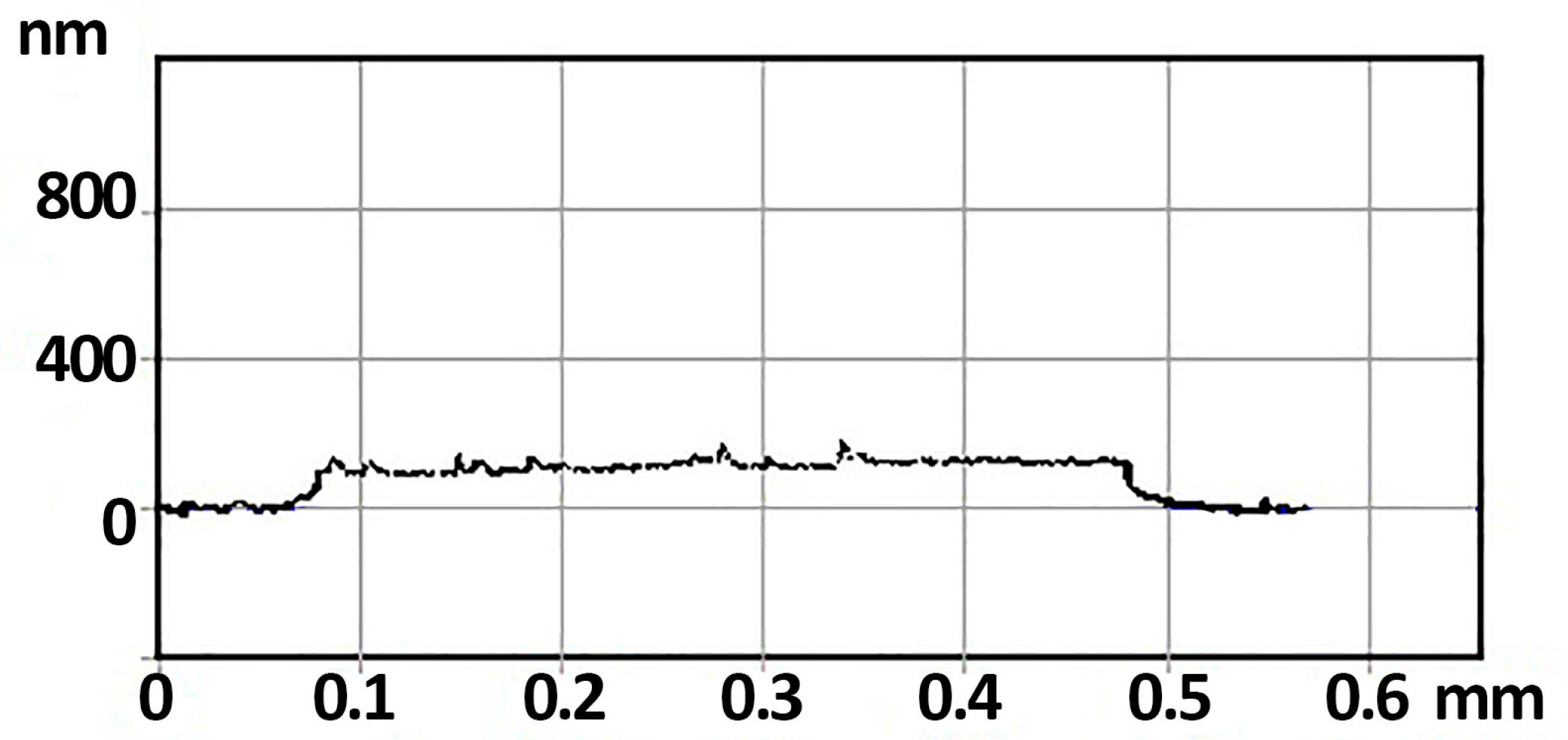
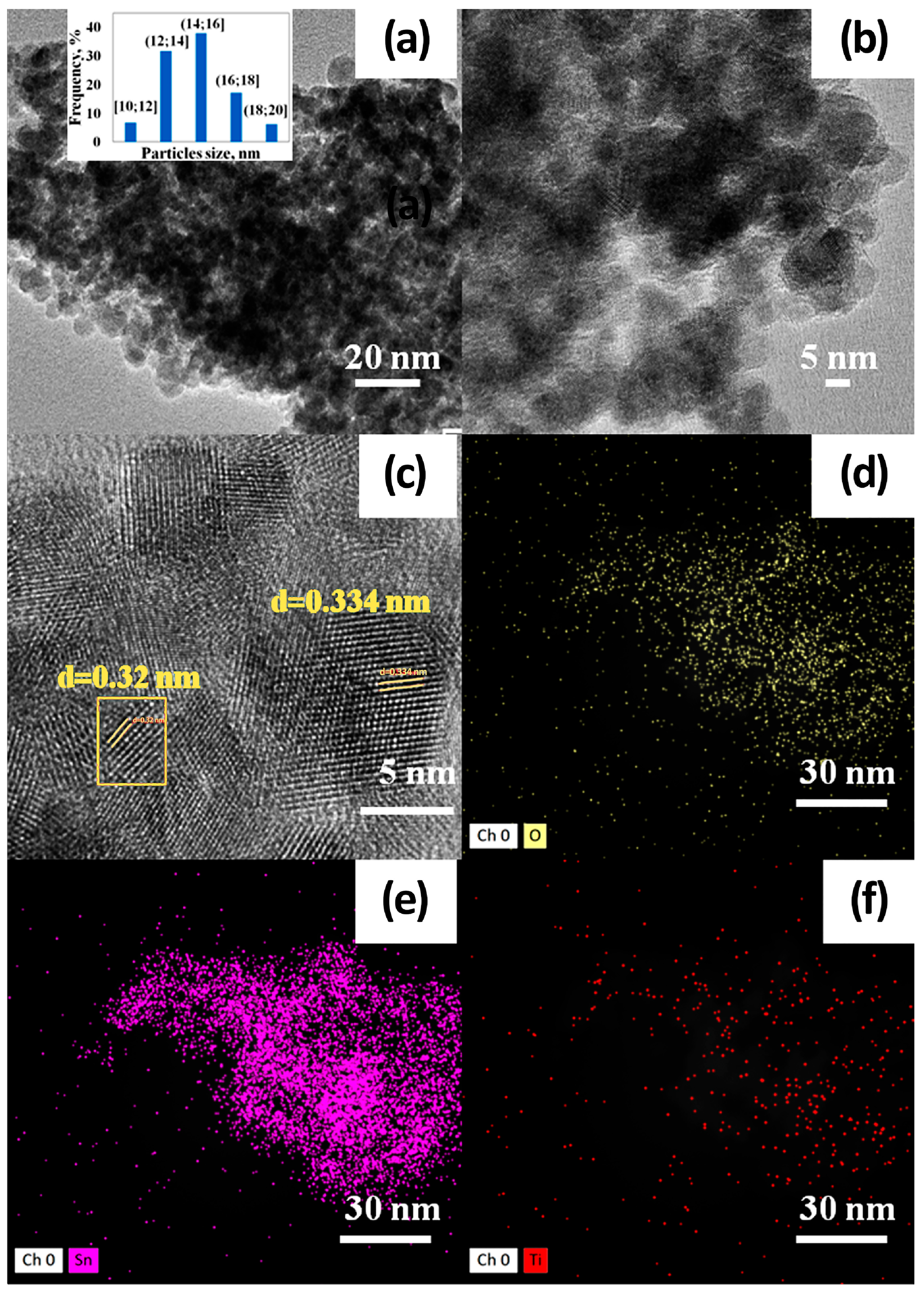
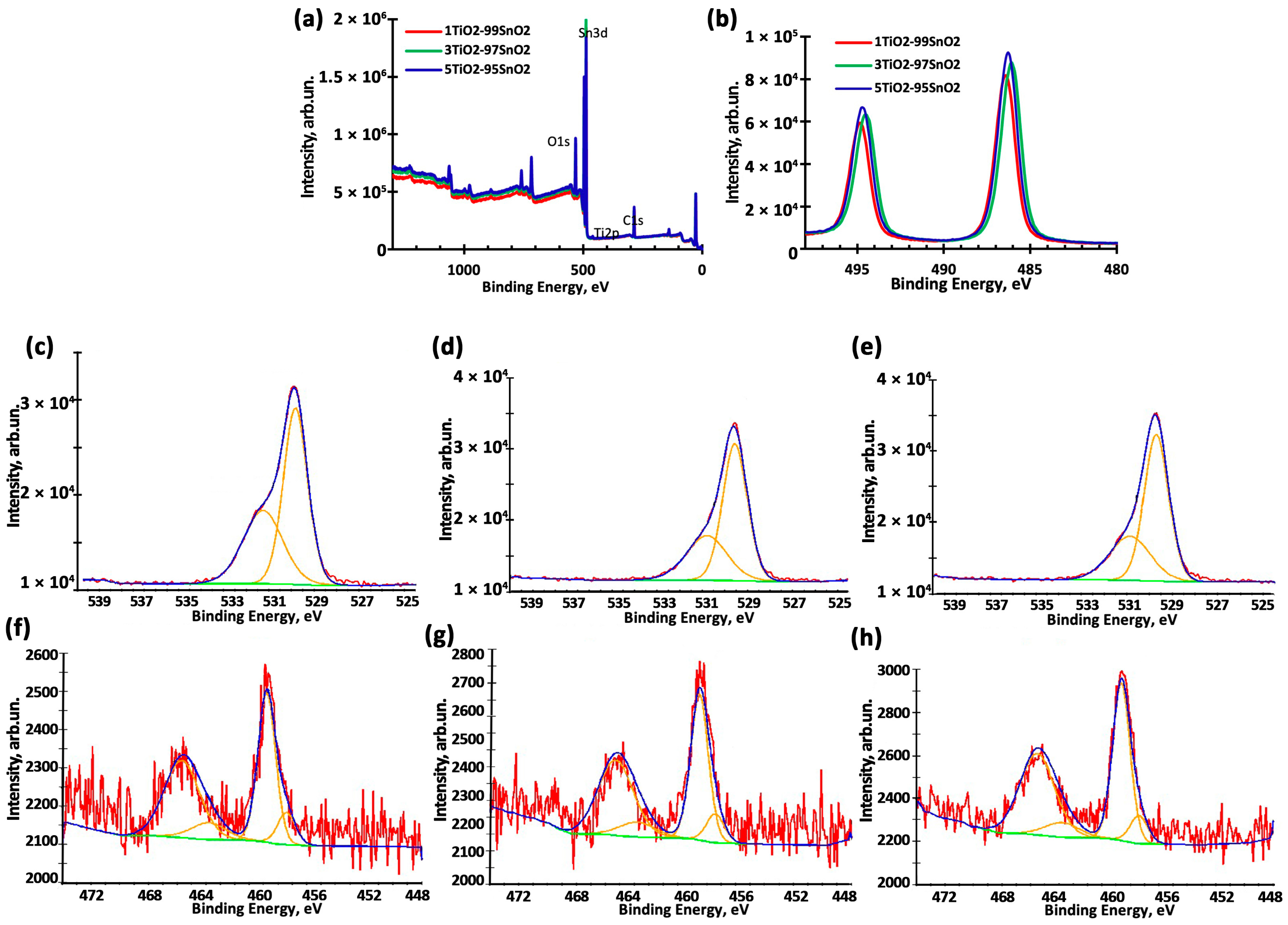
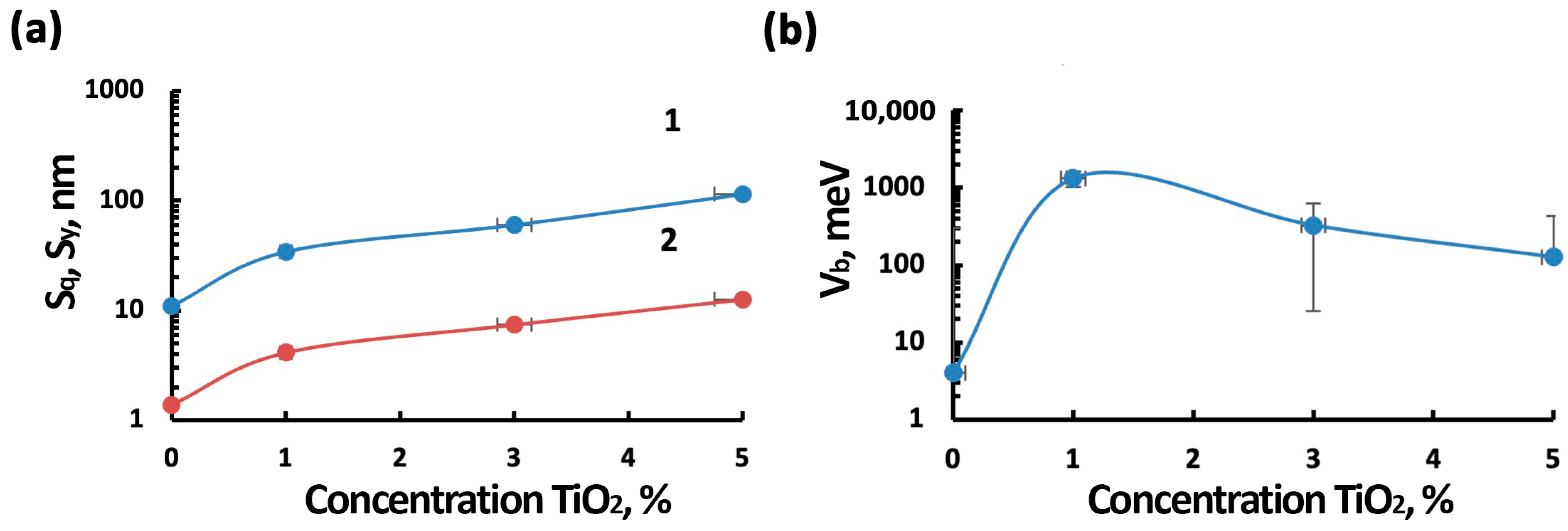
3.1. Morphology, Structure, and Elemental Composition Analysis
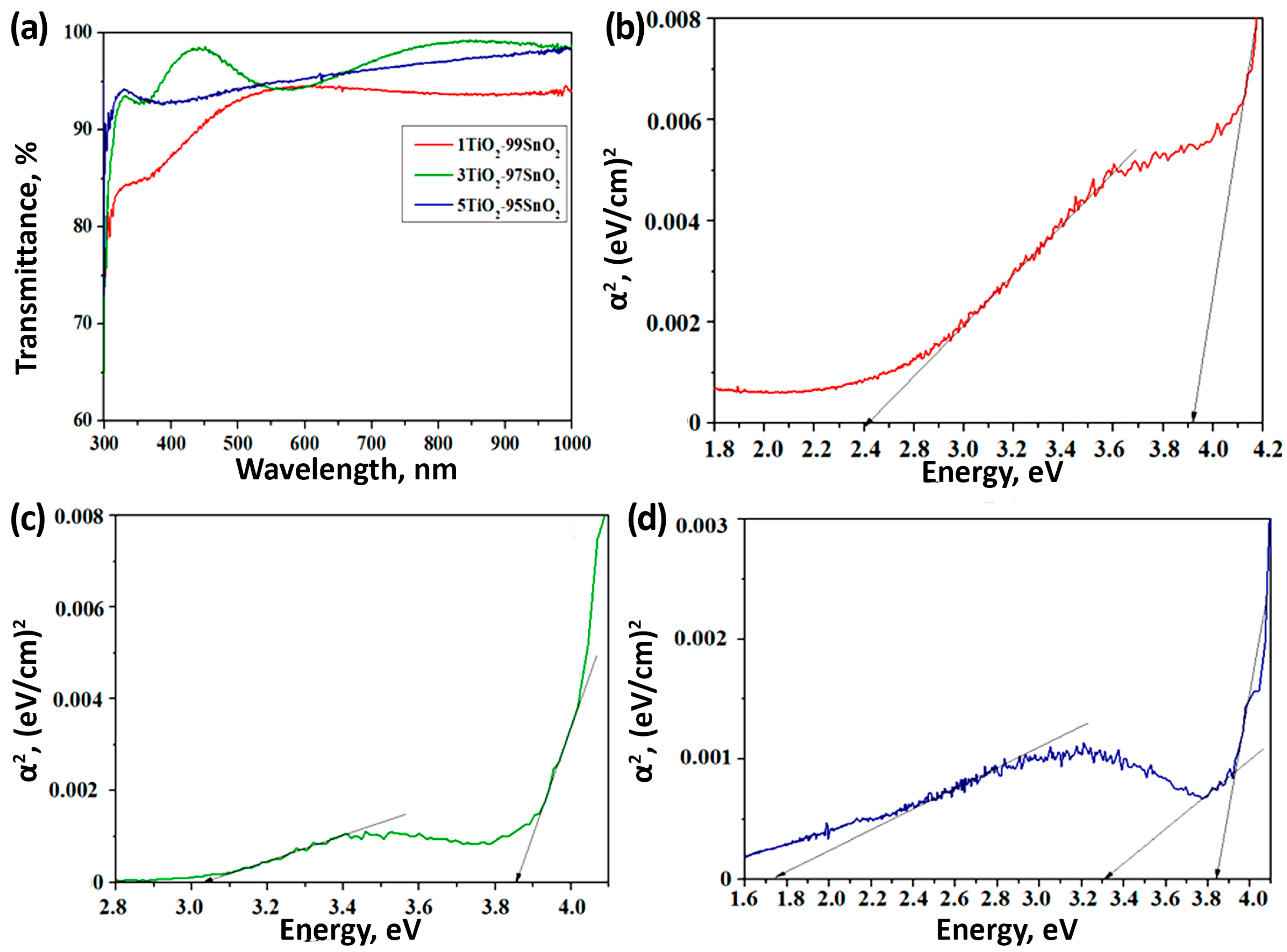
3.2. Optical Properties
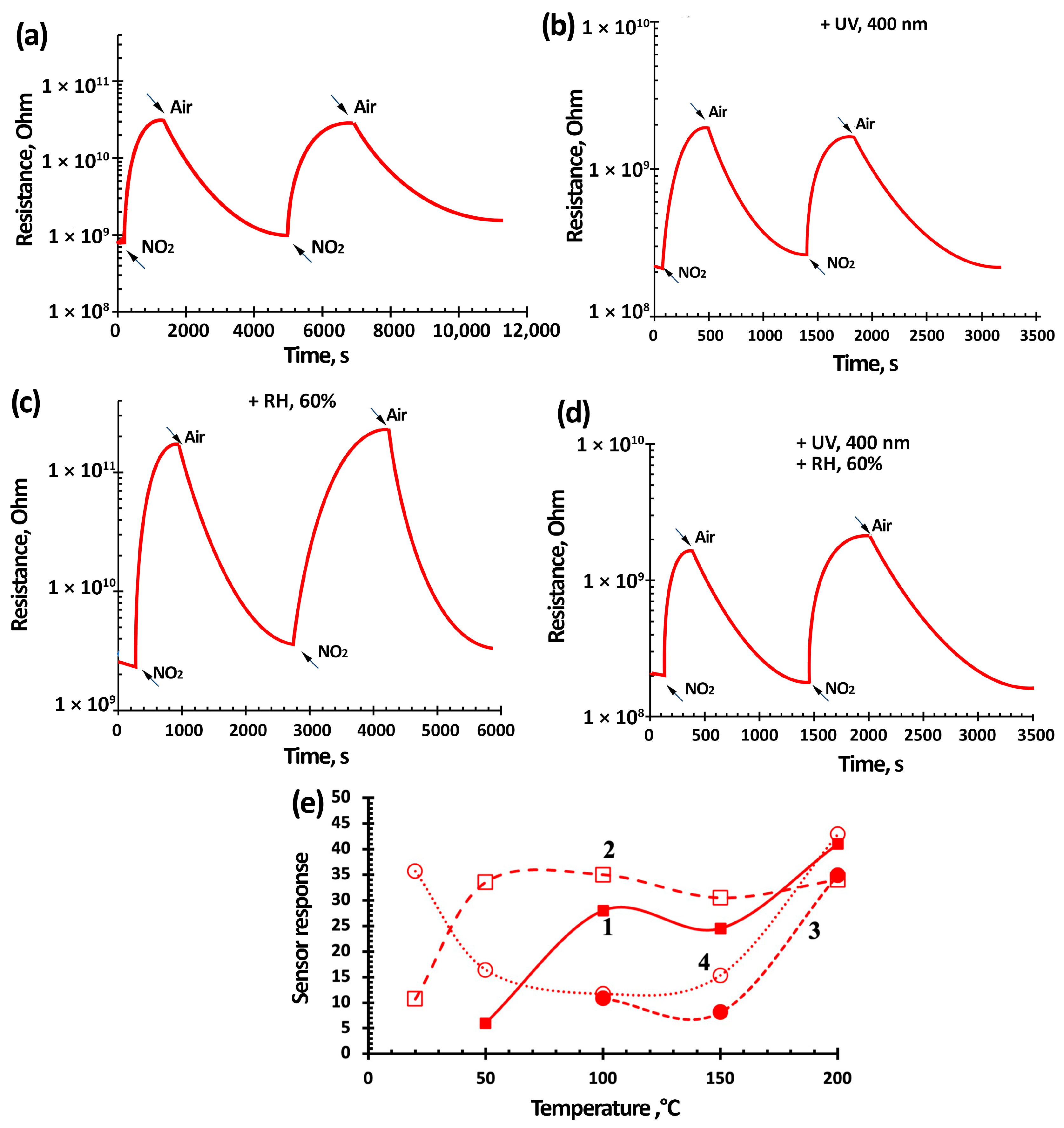
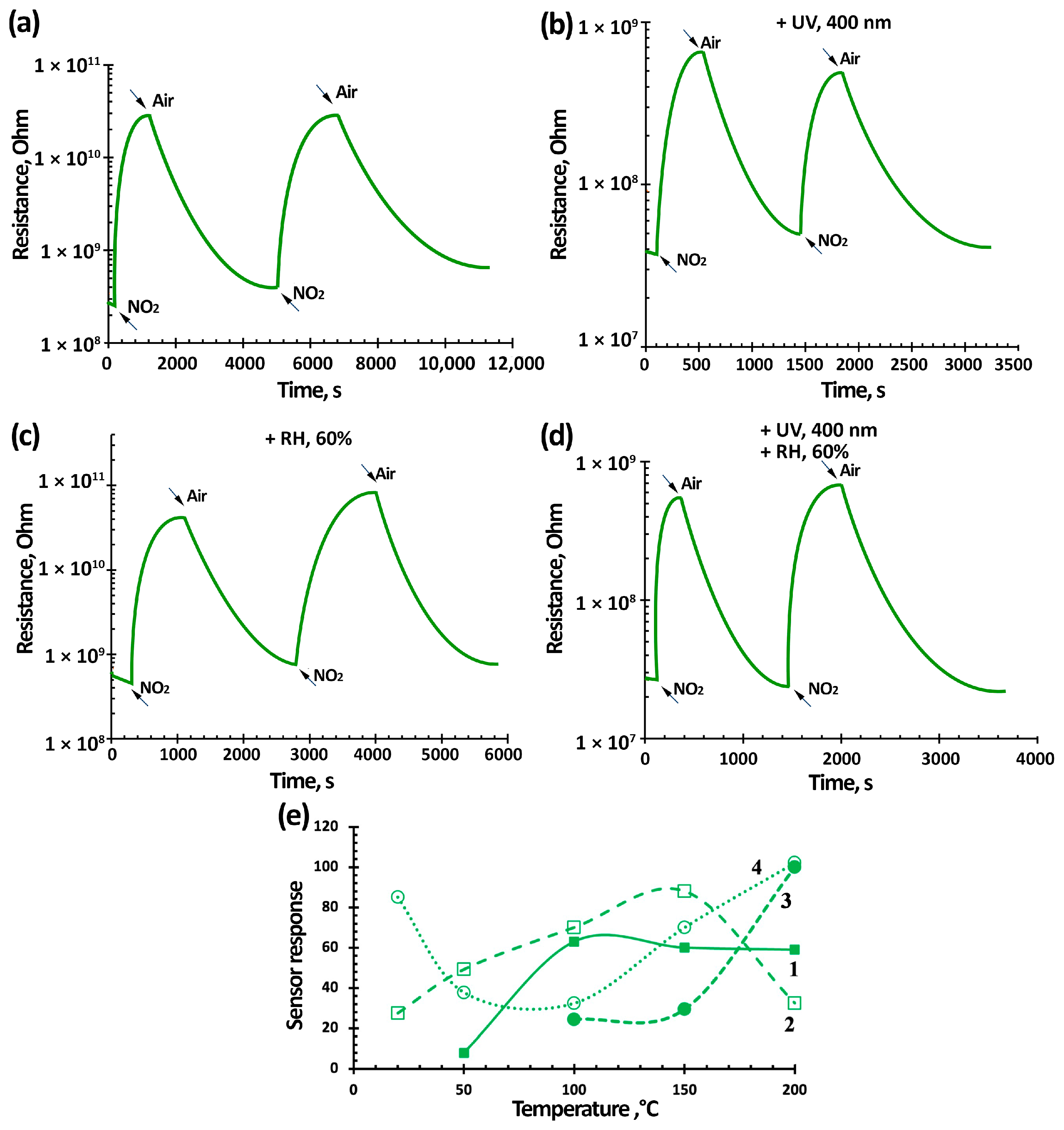
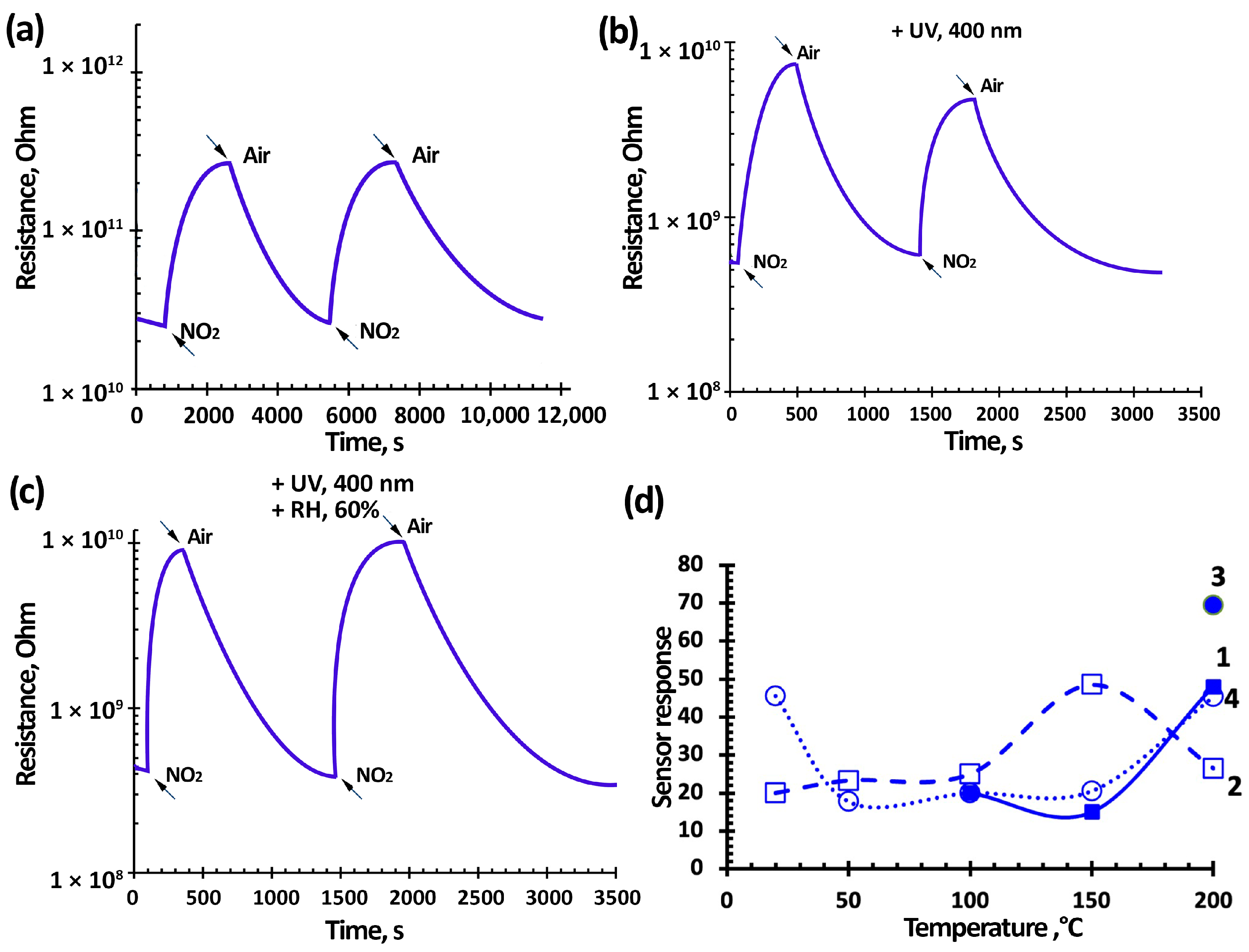
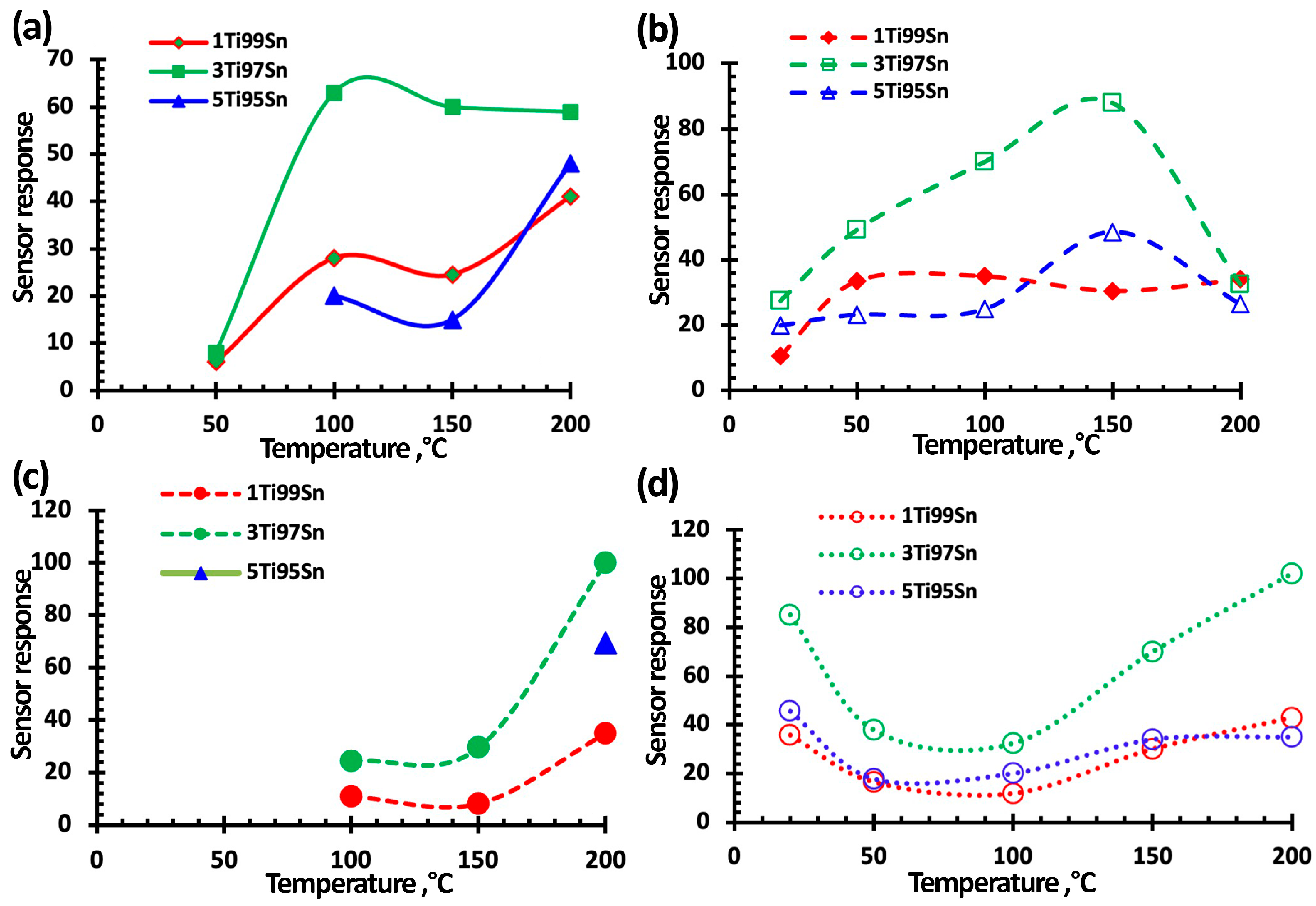
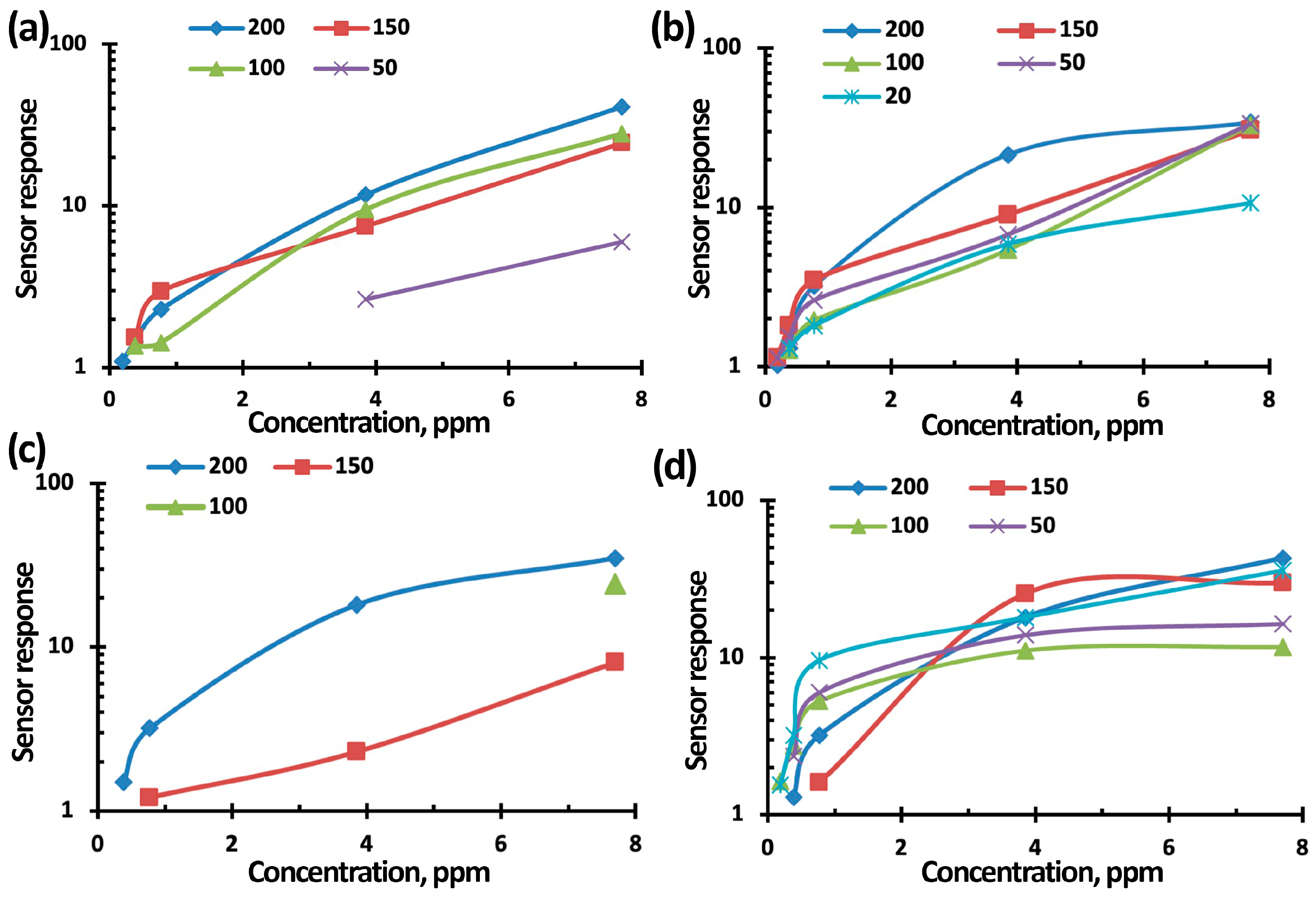
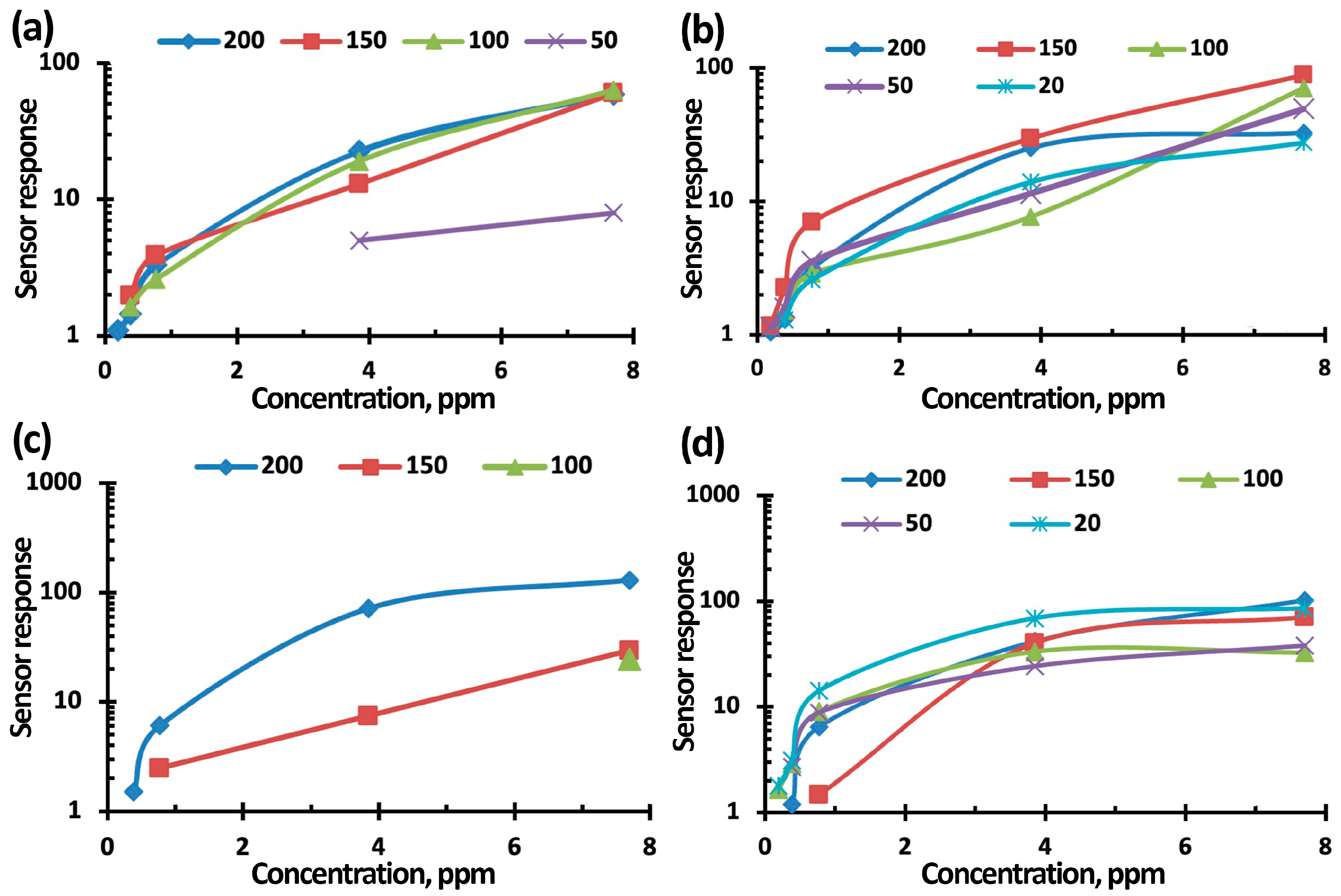
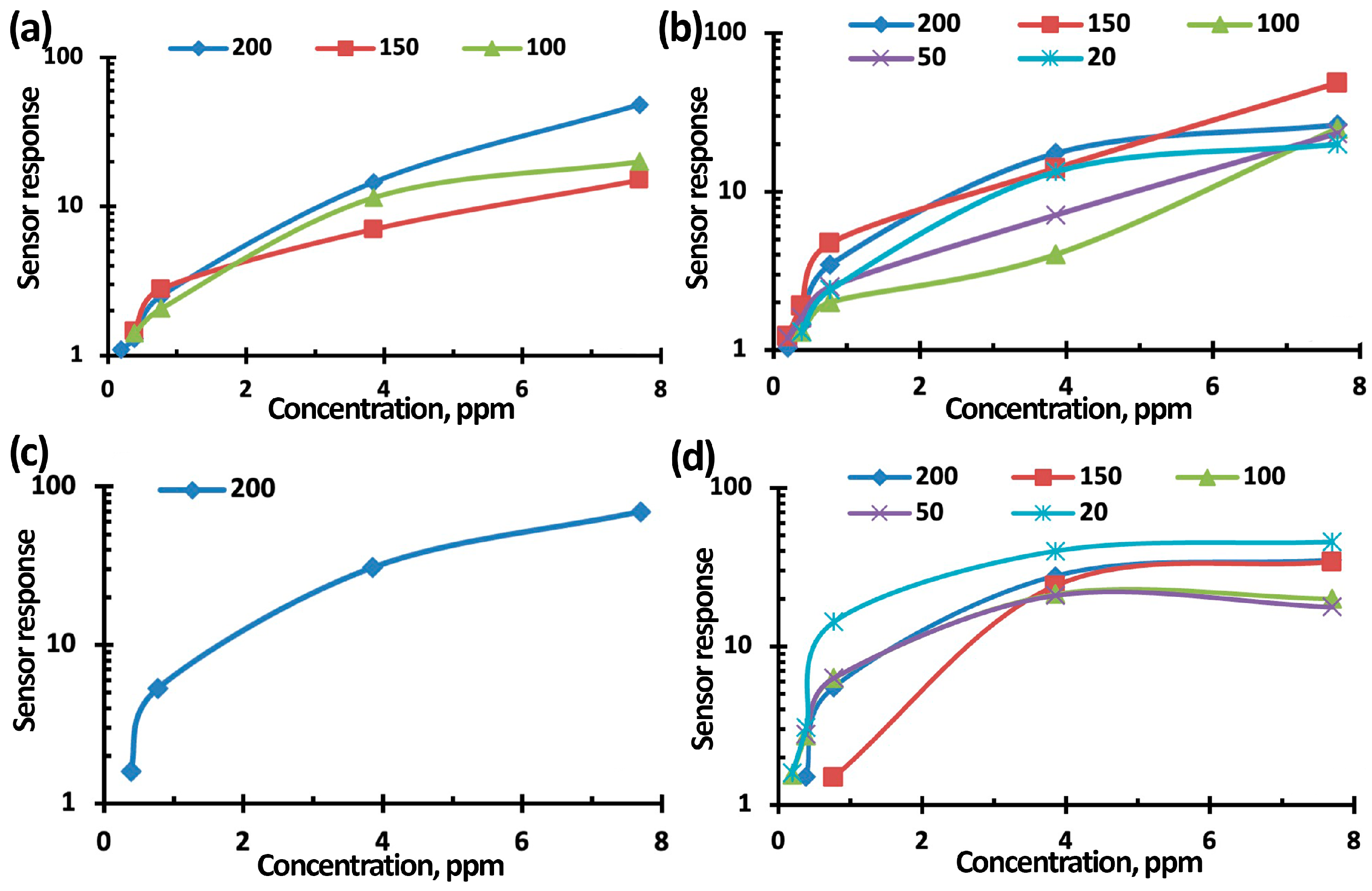
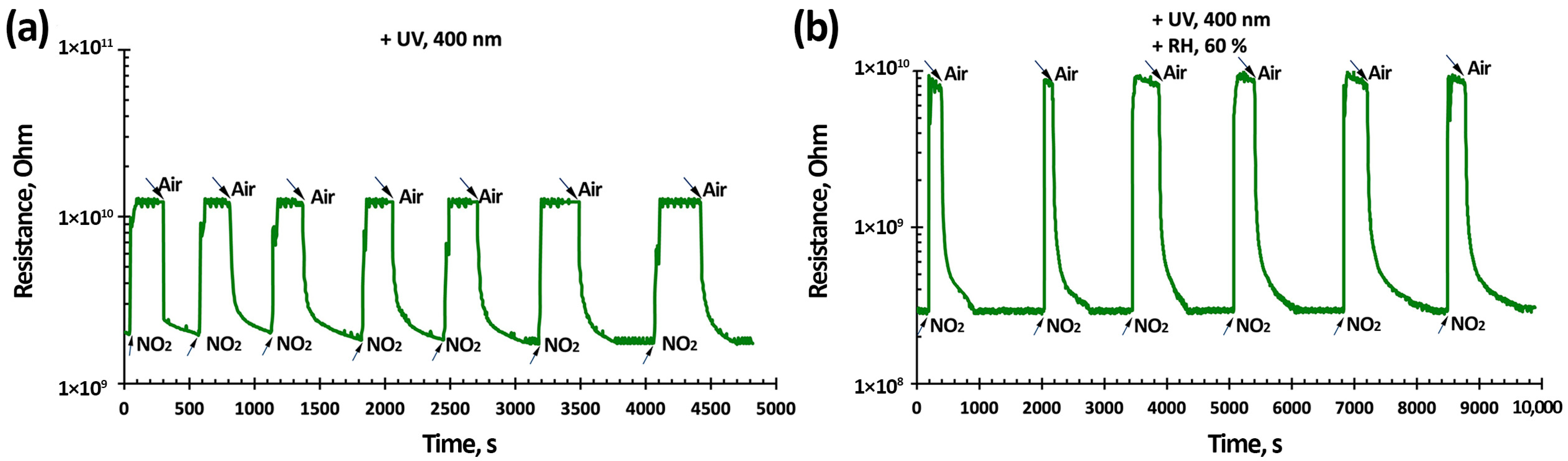
3.3. NO2 Gas-Sensing Performance of TiO2-SnO2-Based Gas Sensors
4. Conclusions
Supplementary Materials
Author Contributions
Funding
Data Availability Statement
Acknowledgments
Conflicts of Interest
References
- Xu, J.; He, X.; Xu, K.; Liao, H.; Zhang, C. Synthesis and Optimization Strategies of Nanostructured Metal Oxides for Chemiresistive Methanol Sensors. Ceram. Int. 2023, 49, 21113–21132. [Google Scholar] [CrossRef]
- Moon, Y.K.; Jeong, S.Y.; Jo, Y.M.; Jo, Y.K.; Kang, Y.C.; Lee, J.H. Highly Selective Detection of Benzene and Discrimination of Volatile Aromatic Compounds Using Oxide Chemiresistors with Tunable Rh-TiO2 Catalytic Overlayers. Adv. Sci. 2021, 8, 2004078. [Google Scholar] [CrossRef] [PubMed]
- Krishna, K.G.; Parne, S.; Pothukanuri, N.; Kathirvelu, V.; Gandi, S.; Joshi, D. Nanostructured Metal Oxide Semiconductor-Based Gas Sensors: A Comprehensive Review. Sens. Actuators Phys. 2022, 341, 113578. [Google Scholar] [CrossRef]
- Zhang, C.; Liu, G.; Geng, X.; Wu, K.; Debliquy, M. Metal Oxide Semiconductors with Highly Concentrated Oxygen Vacancies for Gas Sensing Materials: A Review. Sens. Actuators Phys. 2020, 309, 112026. [Google Scholar] [CrossRef]
- Wang, M.; Zhu, Y.; Luo, Q.; Ge, C.; Liu, G.; Qiao, G.; Kim, E.J. Below-Room-Temperature Solution-Grown ZnO Porous Nanosheet Arrays with Ppb-Level NO2 Sensitivity under Intermittent UV Irradiation. Appl. Surf. Sci. 2021, 566, 150750. [Google Scholar] [CrossRef]
- Chizhov, A.; Rumyantseva, M.; Gaskov, A. Light activation of nanocrystalline metal oxides for gas sensing: Principles, achievements, challenges. Nanomaterials. 2021, 11, 892. [Google Scholar] [CrossRef]
- Wang, J.; Shen, H.; Xia, Y.; Komarneni, S. Light-activated room-temperature gas sensors based on metal oxide nanostructures: A review on recent advances. Ceram. Int. 2021, 47, 7353–7368. [Google Scholar] [CrossRef]
- Das, S.; Mojumder, S.; Saha, D.; Pal, M. Influence of major parameters on the sensing mechanism of semiconductor metal oxide based chemiresistive gas sensors: A review focused on personalized healthcare. Sens. Actuators Chem. 2022, 352, 131066. [Google Scholar] [CrossRef]
- Xu, F.; Ho, H.P. Light-activated metal oxide gas sensors: A review. Micromachines 2017, 8, 333. [Google Scholar] [CrossRef]
- Li, Z.; Zeng, W.; Li, Q. SnO2 as a gas sensor in detection of volatile organic compounds: A review. Sens. Actuators Phys. 2022, 346, 113845. [Google Scholar] [CrossRef]
- Masuda, Y. Recent Advances in SnO2 Nanostructure Based Gas Sensors. Sens. Actuators B Chem. 2022, 364, 131876. [Google Scholar] [CrossRef]
- Gerasimov, G.N.; Gromov, V.F.; Ikim, M.I.; Ilegbusi, O.J.; Ozerin, S.A.; Trakhtenberg, L.I. Structure and Gas-Sensing Properties of SnO2-In2O3 Nanocomposites Synthesized by Impregnation Method. Sens. Actuators B Chem. 2020, 320, 128406. [Google Scholar] [CrossRef]
- Petrov, V.V.; Ivanishcheva, A.P.; Volkova, M.G.; Storozhenko, V.Y.; Gulyaeva, I.A.; Pankov, I.V.; Volochaev, V.A.; Khubezhov, S.A.; Bayan, E.M. High Gas Sensitivity to Nitrogen Dioxide of Nanocomposite ZnO-SnO2 Films Activated by a Surface Electric Field. Nanomaterials 2022, 12, 2025. [Google Scholar] [CrossRef] [PubMed]
- Li, A.; Zhao, S.; Bai, J.; Gao, S.; Wei, D.; Shen, Y.; Yuan, Z.; Meng, F. Optimal construction and gas sensing properties of SnO2@TiO2 heterostructured nanorods. Sens. Actuators B Chem. 2022, 355, 131261. [Google Scholar] [CrossRef]
- Yang, H. A Short Review on Heterojunction Photocatalysts: Carrier Transfer Behavior and Photocatalytic Mechanisms. Mater. Res. Bull. 2021, 142, 111406. [Google Scholar] [CrossRef]
- Kumar, R.; Liu, X.; Zhang, J.; Kumar, M. Room-Temperature Gas Sensors Under Photoactivation: From Metal Oxides to 2D Materials. Nano-Micro Lett. 2020, 12, 164. [Google Scholar] [CrossRef]
- Maziarz, W. TiO2/SnO2 and TiO2/CuO thin film nano-heterostructures as gas sensors. Appl. Surf. Sci. 2019, 480, 361–370. [Google Scholar] [CrossRef]
- Xu, H.; Ju, J.; Li, W.; Zhang, J.; Wang, J.; Cao, B. Superior Triethylamine-Sensing Properties Based on TiO2/SnO2 n–n Heterojunction Nanosheets Directly Grown on Ceramic Tubes. Sens. Actuators B Chem. 2016, 228, 634–642. [Google Scholar] [CrossRef]
- Jin, C.; Park, S.; Kim, H.; Ko, T.; Lee, C.; Jeong, B.-Y. Enhanced NO2 gas-sensing properties of SnO2 nanorods with a TiO2 capping. J. Korean Chem. Soc. 2012, 61, 1370–1375. [Google Scholar] [CrossRef]
- Sharma, S.; Kumar, N.; Makgwane, P.R.; Chauhan, N.S.; Kumari, K.; Rani, M.; Maken, S. TiO2/SnO2 Nano-Composite: New Insights in Synthetic, Structural, Optical and Photocatalytic Aspects. Inorganica Chim. Acta 2022, 529, 120640. [Google Scholar] [CrossRef]
- Zakrzewska, K.; Radecka, M.; Przewoźnik, J.; Kowalski, K.; Czuba, P. Microstructure and photoelectrochemical characterization of the TiO2–SnO2 system. Thin Solid Film. 2005, 490, 101–107. [Google Scholar] [CrossRef]
- Radecka, M.; Przewoźnik, J.; Zakrzewska, K. Microstructure and gas-sensing properties of (Sn,Ti)O2 thin films deposited by RGTO technique. Thin Solid Film. 2001, 391, 247–254. [Google Scholar] [CrossRef]
- Medjaldi, F.; Bouabellou, A.; Bouachiba, Y.; Taabouche, A.; Bouatia, K.; Serrar, H. Study of TiO2, SnO2 and Nanocomposites TiO2:SnO2 Thin Films Prepared by Sol-Gel Method: Successful Elaboration of Variable–Refractive Index Systems. Mater. Res. Express 2020, 7, 016439. [Google Scholar] [CrossRef]
- Sabri, Y.M.; Kandjani, A.E.; Rashid, S.S.A.A.H.; Harrison, C.J.; Ippolito, S.J.; Bhargava, S.K. Soot template TiO2 fractals as a photoactive gas sensor for acetone detection. Sens. Actuators B Chem. 2018, 275, 215–222. [Google Scholar] [CrossRef]
- Li, G.; Sun, Z.; Zhang, D.; Xu, Q.; Meng, L.; Qin, Y. Mechanism of Sensitivity Enhancement of a ZnO Nanofilm Gas Sensor by UV Light Illumination. ACS Sens. 2019, 4, 1577–1585. [Google Scholar] [CrossRef]
- Ganesh Moorthy, S.; Bouvet, M. Effects of Visible Light on Gas Sensors: From Inorganic Resistors to Molecular Material-Based Heterojunctions. Sensors 2024, 24, 1571. [Google Scholar] [CrossRef]
- Zhang, S.; Zhao, L.; Huang, B.; Li, X. UV-Activated Formaldehyde Sensing Properties of Hollow TiO2@SnO2 Heterojunctions at Room Temperature. Sens. Actuators B Chem. 2020, 319, 128264. [Google Scholar] [CrossRef]
- Shang, R.; Huang, H.; Liu, C.; Wang, M. UV-Activated TiO2/SnO2 Oxygen Sensor with Improved Response Speed for Low Temperature and Air-Atmospheric Operation. Sens. Actuators B Chem. 2025, 425, 136947. [Google Scholar] [CrossRef]
- Krylov, O.V. Heterogeneous Catalysis; ICTS “Akademkniga”: Moscow, Russia, 2004. [Google Scholar]
- Wang, Y.-D.; Wu, X.-H.; Su, Q.; Li, Y.-F.; Zhou, Z.-L. Ammonia-Sensing Characteristics of Pt and SiO2 Doped SnO2 Materials. Solid-State Electron. 2001, 45, 347–350. [Google Scholar] [CrossRef]
- Comini, E. Electrical Properties of Tin Dioxide Two-Dimensional Nanostructures. J. Phys. Chem. B 2004, 108, 1882–1887. [Google Scholar] [CrossRef]
- Herrmann, J.M.; Disdier, J.; Fernandez, A.; Jimenez, V.M.; Sanchez-Lopez, J.C. Oxygen gas sensing behavior of nanocrystalline tin oxide prepared by the gas phase condensation method. Nanostruct. Mater. 1997, 8, 675–686. [Google Scholar] [CrossRef]
- Fan, S.W.; Srivastava, A.K.; Dravid, V.P. UV-activated room-temperature gas sensing mechanism of polycrystalline ZnO. Appl. Phys. Lett. 2009, 95, 142106. [Google Scholar] [CrossRef]
- Wang, J.; Deng, H.; Li, X.; Yang, C.; Xia, Y. Visible-Light Photocatalysis Enhanced Room-Temperature Formaldehyde Gas Sensing by MoS2/rGO Hybrids. Sens. Actuators B Chem. 2020, 304, 127317. [Google Scholar] [CrossRef]
- Kim, S.; Cho, D.-H.; Chang, H.-K.; Lee, H.-N.; Kim, H.-J.; Park, T.J.; Park, Y.M. Selective Photoactive Gas Detection of CO and HCHO Using Highly Porous SnO2 and SnO2@TiO2 Heterostructure. Sens. Actuators B Chem. 2022, 358, 131486. [Google Scholar] [CrossRef]
- Gaskov, A.M.; Rumyantseva, M.N. Selection Of Materials For Solid-State Gas Sensors. Inorg. Mater. 2000, 36, 369–378. [Google Scholar]
- Emiroglu, S.; Barsan, N.; Weimar, U.; Hoffmann, V. In situ diffuse reflectance infrared spectroscopy study of CO adsorption on SnO2. Thin Solid Film. 2001, 391, 176–185. [Google Scholar] [CrossRef]
- Platonov, V.; Malinin, N.; Vasiliev, R.; Rumyantseva, M. Room Temperature UV-Activated NO2 and NO Detection by ZnO/rGO Composites. Chemosensors 2023, 11, 227. [Google Scholar] [CrossRef]
- Starnikova, A.; Petrov, V. Electrical Properties of ZnO/Au and ZnO/SnO2 Nanorod Arrays When Exposed to UV Irradiation with Controlled Intensity. Phys. Math. 2024, 17, 373. [Google Scholar] [CrossRef]
- Petrov, V.V.; Sysoev, V.V.; Ignatieva, I.O.; Gulyaeva, I.A.; Volkova, M.G.; Ivanishcheva, A.P.; Khubezhov, S.A.; Varzarev, Y.N.; Bayan, E.M. Nanocomposite Co3O4-ZnO Thin Films for Photoconductivity Sensors. Sensors 2023, 23, 5617. [Google Scholar] [CrossRef]
- Petrov, V.V.; Ignatieva, I.O.; Volkova, M.G.; Gulyaeva, I.A.; Pankov, I.V.; Bayan, E.M. Polycrystalline Transparent Al-Doped ZnO Thin Films for Photosensitivity and Optoelectronic Applications. Nanomaterials 2023, 13, 2348. [Google Scholar] [CrossRef]
- Li, Q.; Zeng, W.; Li, Y. Metal Oxide Gas Sensors for Detecting NO2 in Industrial Exhaust Gas: Recent Developments. Sens. Actuators B Chem. 2022, 359, 131579. [Google Scholar] [CrossRef]
- Deb, M.; Ghossoub, Y.; Noel, L.; Li, P.-H.; Tsai, H.-Y.; Soppera, O.; Zan, H.-W. Highly Efficient UV-Activated TiO2 /SnO2 Surface Nano-Matrix Gas Sensor: Enhancing Stability for Ppb-Level NO x Detection at Room Temperature. ACS Appl. Mater. Interfaces 2025, 17, 14670–14681. [Google Scholar] [CrossRef] [PubMed]
- Volkova, M.G.; Storozhenko, V.Y.; Gulyaeva, I.A.; Starnikova, A.P.; Petrov, V.V.; Bayan, E.M. TiO2-SnO2 Films: Synthesis by Low-Temperature Pyrolysis and Electrophysical Properties. Mater. Today Proc. 2022, 52, 187–190. [Google Scholar] [CrossRef]
- Shalimova, K.V. Physics of Semiconductors; Energiya: Korolyov, Russia, 1976. [Google Scholar]
- Volkova, M.G.; Storozhenko, V.Y.; Petrov, V.V.; Bayan, E.M. Structural properties of TiO2-SnO2 thin films prepared by new pyrolysis solid-phase method. J. Phys. Conf. Ser. 2021, 2086, 012042. [Google Scholar] [CrossRef]
- Liu, Q.; Zhan, H.; Huang, X.; Song, Y.; He, S.; Li, X.; Wang, C.; Xie, Z. High Visible Light Photocatalytic Activity of SnO2-x Nanocrystals with Rich Oxygen Vacancy. Eur. J. Inorg. Chem. 2021, 2021, 4370. [Google Scholar] [CrossRef]
- Mantilla, Á.; Guerrero-Araque, D.; Sierra-Uribe, J.H.; Lartundo-Rojas, L.; Gómez, R.; Calderon, H.A.; Zanella, R.; Ramírez-Ortega, D. Highly Efficient Mobility, Separation and Charge Transfer in Black SnO2–TiO2 Structures with Co-Catalysts: The Key Step for the Photocatalytic Hydrogen Evolution. RSC Adv. 2024, 14, 26259–26271. [Google Scholar] [CrossRef]
- Gulyaeva, I.; Ivanishcheva, A.; Volkova, M.; Bayan, E. Surface and Electrophysical Properties Study of Thin TiO2 -SnO2 Nanocomposite Films. Phys. Math. 2022, 15, 386. [Google Scholar] [CrossRef]
- Kohl, D. Surface processes in the detection of reducing gases with SnO2-based devices. Sens. Actuators. 1989, 18, 71–113. [Google Scholar] [CrossRef]
- Kuznetsov, V.N.; Serpone, N. On the Origin of the Spectral Bands in the Visible Absorption Spectra of Visible-Light-Active TiO2 Specimens Analysis and Assignments. J. Phys. Chem. C 2009, 113, 15110–15123. [Google Scholar] [CrossRef]
- Rembeza, S.I.; Svistova, T.V.; Rembeza, E.S.; Borsyakova, O.I. The microstructure and physical properties of thin SnO2 films. Semiconductors 2001, 35, 762–765. [Google Scholar] [CrossRef]
- Yang, Z.; Homewood, K.; Finney, M.; Harry, M.; Reeson, K. Optical Absorption Study of Ion Beam Synthesized Polycrystalline Semiconducting FeSi2. J. Appl. Phys. 1995, 78, 1958–1963. [Google Scholar] [CrossRef]
- McAleer, J.F.; Moseley, P.T.; Norris, J.O.W.; Williams, D.E. Tin dioxide gas sensors. Part 1.—Aspects of the surface chemistry revealed by electrical conductance variations. J. Chem. Soc. Faraday Trans. 1 1987, 83, 1323–1346. [Google Scholar] [CrossRef]
- Egashira, M.; Nakashima, M.; Kawasumi, S.; Selyama, T. Temperature Programmed Desorption Study of Water Adsorbed on Metal Oxides. 2. Tin Oxide Surfaces. J. Phys. Chem. 1981, 85, 4125–4130. [Google Scholar] [CrossRef]
- Barsan, N.; Schweizer-Berberich, M.; Göpel, W. Fundamental and practical aspects in the design of nanoscaled SnO2 gas sensors: A status report. Fresenius J. Anal. Chem. 1999, 365, 287–304. [Google Scholar] [CrossRef]
- Orlandi, M.O. (Ed.) Tin Oxide Materials: Synthesis, Properties, and Applications; Elsevier: Amsterdam, The Netherlands, 2019. [Google Scholar]
- Bandura, A.V.; Sofo, J.O.; Kubicki, J.D. Derivation of Force Field Parameters for SnO2 −H2O Surface Systems from Plane-Wave Density Functional Theory Calculations. J. Phys. Chem. B 2006, 110, 8386–8397. [Google Scholar] [CrossRef]
- Petrov, V.V. Investigation of the interaction features of gas molecules with the surface of oxide gas-sensitive materials. Nano- Microsyst. Eng. 2007, 1, 24–27. [Google Scholar]
- Miyauchi, M.; Nakajima, A.; Watanabe, T.; Hashimoto, K. Photocatalysis and Photoinduced Hydrophilicity of Various Metal Oxide Thin Films. Chem. Mater. 2002, 14, 2812–2816. [Google Scholar] [CrossRef]
- Borodin, A.; Reichling, M. Characterizing TiO2(110) Surface States by Their Work Function. Phys. Chem. Chem. Phys. 2011, 13, 15442. [Google Scholar] [CrossRef]
- Anothainart, K.; Burgmair, M.; Karthigeyan, A.; Zimmer, M.; Eisele, I. Light Enhanced NO2 Gas Sensing with Tin Oxide at Room Temperature: Conductance and Work Function Measurements. Sens. Actuators B Chem. 2003, 93, 580–584. [Google Scholar] [CrossRef]
- Liu, B.; Luo, Y.; Li, K.; Wang, H.; Gao, L.; Duan, G. Room-Temperature NO2 Gas Sensing with Ultra-Sensitivity Activated by Ultraviolet Light Based on SnO2 Monolayer Array Film. Adv. Mater. Interfaces 2019, 6, 1900376. [Google Scholar] [CrossRef]
- Comini, E.; Faglia, G.; Sberveglieri, G. UV Light Activation of Tin Oxide Thin Films for NO2 Sensing at Low Temperatures. Sens. Actuators B Chem. 2001, 78, 73–77. [Google Scholar] [CrossRef]
- Shao, M.; Liu, J.; Ding, W.; Wang, J.; Dong, F.; Zhang, J. Oxygen vacancy engineering of self-doped SnO2−x nanocrystals for ultrasensitive NO2 detection. J. Mater. Chem. C 2020, 8, 487–494. [Google Scholar] [CrossRef]
- Duoc, V.T.; Hung, C.M.; Nguyen, H.; Duy, N.V.; Hieu, N.V.; Hoa, N.D. Room Temperature Highly Toxic NO2 Gas Sensors Based on Rootstock/Scion Nanowires of SnO2/ZnO, ZnO/SnO2, SnO2/SnO2 and, ZnO/ZnO. Sens. Actuators B Chem. 2021, 348, 130652. [Google Scholar] [CrossRef]
- Çorlu, T.; Tekin, S.; Karaduman Er, I.; Acar, S. Room-Temperature Gas Sensing Properties of Zn, Sn and Cu-Doped TiO2 Films. J. Mater. Sci. Mater. Electron. 2023, 34, 2224. [Google Scholar] [CrossRef]
- Hyodo, T.; Urata, K.; Kamada, K.; Ueda, T.; Shimizu, Y. Semiconductor-Type SnO2-Based NO2 Sensors Operated at Room Temperature under UV-Light Irradiation. Sens. Actuators B Chem. 2017, 253, 630–640. [Google Scholar] [CrossRef]
- Liaqat, M.J.; Hussain, S.; Shahid, A.; Amu-Darko, J.N.O.; Ibrahim, T.K.; Ibrahim, S.M.; Manavalan, R.K.; Zhang, X.; Qiao, G.; Liu, G. Hydrothermally Grown WO3-SnO2 Nanocomposites for Efficient NO2 Detection at Low Concentration. Sens. Actuators B Chem. 2025, 436, 137711. [Google Scholar] [CrossRef]
- Nowak, P.; Maziarz, W.; Rydosz, A.; Kowalski, K.; Ziąbka, M.; Zakrzewska, K. SnO2/TiO2 Thin Film n-n Heterostructures of Improved Sensitivity to NO2. Sensors 2020, 20, 6830. [Google Scholar] [CrossRef]

| Sample | O1s | Sn 3d | Ti2p3 (Ti3+) | Ti2p3 (Ti4+) | Concentration of Atoms/Ions | |||||||
|---|---|---|---|---|---|---|---|---|---|---|---|---|
| Ov | Oxide | 3d3\2 | 3d5\2 | 2p3/2 | 2p1/2 | 2p3/2 | 2p1/2 | Sn | Ti | Ti3+ | Ti4+ | |
| 1TiO2–99SnO2 | 531.78 | 530.28 | 494.98 | 486.58 | 457.48 | 462.88 | 457.78 | 464.78 | 98.17 | 1.83 | 17.7 | 82.3 |
| 3TiO2–97SnO2 | 531.20 | 530.08 | 494.48 | 486.18 | 457.38 | 462.88 | 458.48 | 464.28 | 96.44 | 3.56 | 16.5 | 83.5 |
| 5TiO2–95SnO2 | 531.38 | 530.18 | 494.68 | 486.28 | 457.38 | 462.88 | 458.58 | 464.58 | 95.28 | 4.72 | 15.0 | 85.0 |
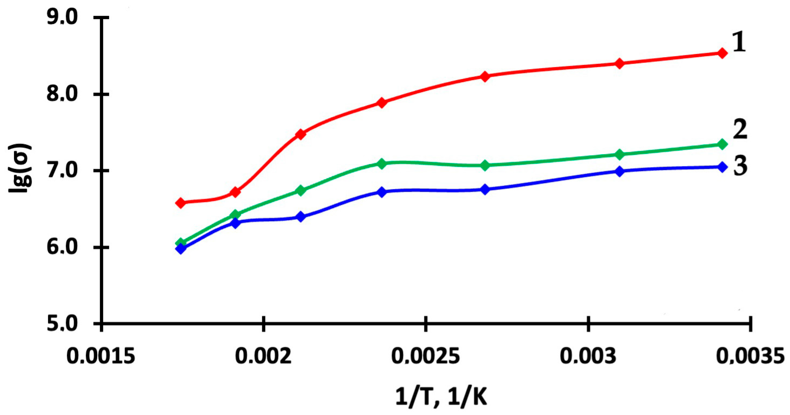
| Thin Film | Ea, eV | Ea, eV (with Light Activation) | |||
|---|---|---|---|---|---|
| 30–120 °C | 120–230 °C | 230–300 °C | 20–150 °C | 150–300 °C | |
| 1TiO2–99SnO2 | 0.33 | 0.56 | 0.51 | 0.12 | 0.42 |
| 3TiO2–97SnO2 | 0.33 | 0.68 | 0.57 | 0.05 | 0.33 |
| 5TiO2–95SnO2 | 0.33 | 0.76 | 0.63 | 0.06 | 0.24 |
| Materials | Synthesis Method | Sensitivity or Response (NO2 Concentration) | Response/Recovery Time, s | Measurement Conditions | References | |
|---|---|---|---|---|---|---|
| Light Source | Temperature, Humidity | |||||
| SnO2 mono-layer array, particle size 20 nm | Hydrothermal | 10 (10 ppm) | - | 365 nm | RT 62% RH | [63] |
| SnO2 nanoparticles | Rheotaxial growth and its thermal oxidation | 20% (1 ppm) | 900/240 | 365 nm | RT, 30% RH | [64] |
| SnO2−x nanocrystals, grain size 10 nm | Hydrothermal | 70 (500 ppb) | 230/88 | - | 100 °C, 26% RH | [65] |
| SnO2/ZnO heterostructure, ZnO nanowires 30–50 nm diameter, SnO2 rootstock 100–110 nm diameter | Thermal evaporation technique | 390 (1 ppm) | - | - | 30 °C | [66] |
| Sn–doped TIO2, nanoparticle size 8 nm | Successive Ionic Layer Adsorption and Reaction Method | 12% (10 ppm) | - | - | RT | [67] |
| 0.05Pd/SnO2 | Chemical method and ultrasonic exposure | 3000 (5 ppm) | 168/108 | 365 nm | [68] | |
| WO3–SnO2 nanocomposites | Hydrothermal method | NO2, 10 ppm, 1167 | 39.51/98.07 | - | 150 °C | [69] |
| Bi-layers SnO2/TiO2 n-n heterostructures | Magnetron sputtering/L–B technique | NO2, 0.2 ppm, 847 | 26/58 | - | 123 °C | [70] |
| NO2, 12 ppm, 881 | - | 150 °C, 50% RH | ||||
| Nanoporous two-layer TiO2/SnO2 | two-step sol–gel process | NO, 4 ppb, 0.6% | 35/85 s | 365 nm, 3 μW/cm2 | RT, 30% RH | [43] |
| NO2, 500 ppb, 21.9% | 100 /320 s | |||||
| 3TiO2–97SnO2 | Oxidative pyrolysis | NO2, 7.7 ppm, 85 | 245/460 s | 400 nm 0.2 mW/cm2 | RT, 60% RH | This work |
| NO2, 0.2 ppm, 1.8 | 144/180 s | |||||
Disclaimer/Publisher’s Note: The statements, opinions and data contained in all publications are solely those of the individual author(s) and contributor(s) and not of MDPI and/or the editor(s). MDPI and/or the editor(s) disclaim responsibility for any injury to people or property resulting from any ideas, methods, instructions or products referred to in the content. |
© 2025 by the authors. Licensee MDPI, Basel, Switzerland. This article is an open access article distributed under the terms and conditions of the Creative Commons Attribution (CC BY) license (https://creativecommons.org/licenses/by/4.0/).
Share and Cite
Petrov, V.V.; Starnikova, A.P.; Volkova, M.G.; Khubezhov, S.A.; Pankov, I.V.; Bayan, E.M. Excellent Room-Temperature NO2 Gas-Sensing Properties of TiO2-SnO2 Composite Thin Films Under Light Activation. Nanomaterials 2025, 15, 871. https://doi.org/10.3390/nano15110871
Petrov VV, Starnikova AP, Volkova MG, Khubezhov SA, Pankov IV, Bayan EM. Excellent Room-Temperature NO2 Gas-Sensing Properties of TiO2-SnO2 Composite Thin Films Under Light Activation. Nanomaterials. 2025; 15(11):871. https://doi.org/10.3390/nano15110871
Chicago/Turabian StylePetrov, Victor V., Aleksandra P. Starnikova, Maria G. Volkova, Soslan A. Khubezhov, Ilya V. Pankov, and Ekaterina M. Bayan. 2025. "Excellent Room-Temperature NO2 Gas-Sensing Properties of TiO2-SnO2 Composite Thin Films Under Light Activation" Nanomaterials 15, no. 11: 871. https://doi.org/10.3390/nano15110871
APA StylePetrov, V. V., Starnikova, A. P., Volkova, M. G., Khubezhov, S. A., Pankov, I. V., & Bayan, E. M. (2025). Excellent Room-Temperature NO2 Gas-Sensing Properties of TiO2-SnO2 Composite Thin Films Under Light Activation. Nanomaterials, 15(11), 871. https://doi.org/10.3390/nano15110871