
Design and Analysis of the Dual-Band Far-Field Super-Resolution Metalens with Large Aperture


Abstract
1. Introduction
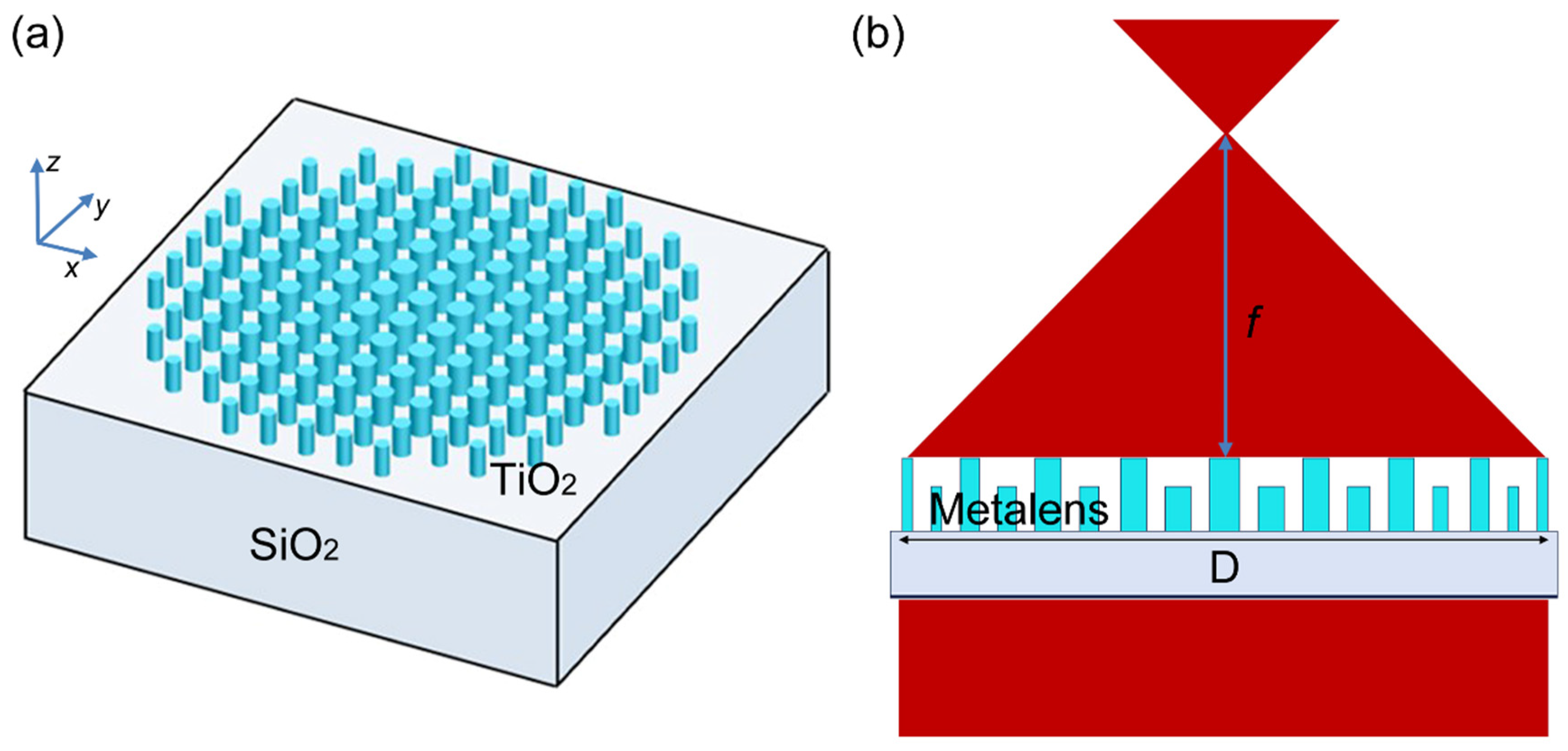
2. Device Design
2.1. The Principle of Device Design
2.2. Confocal Imaging Model of the Dual-Band Metalens with Long Focal Length
3. Result and Discussion
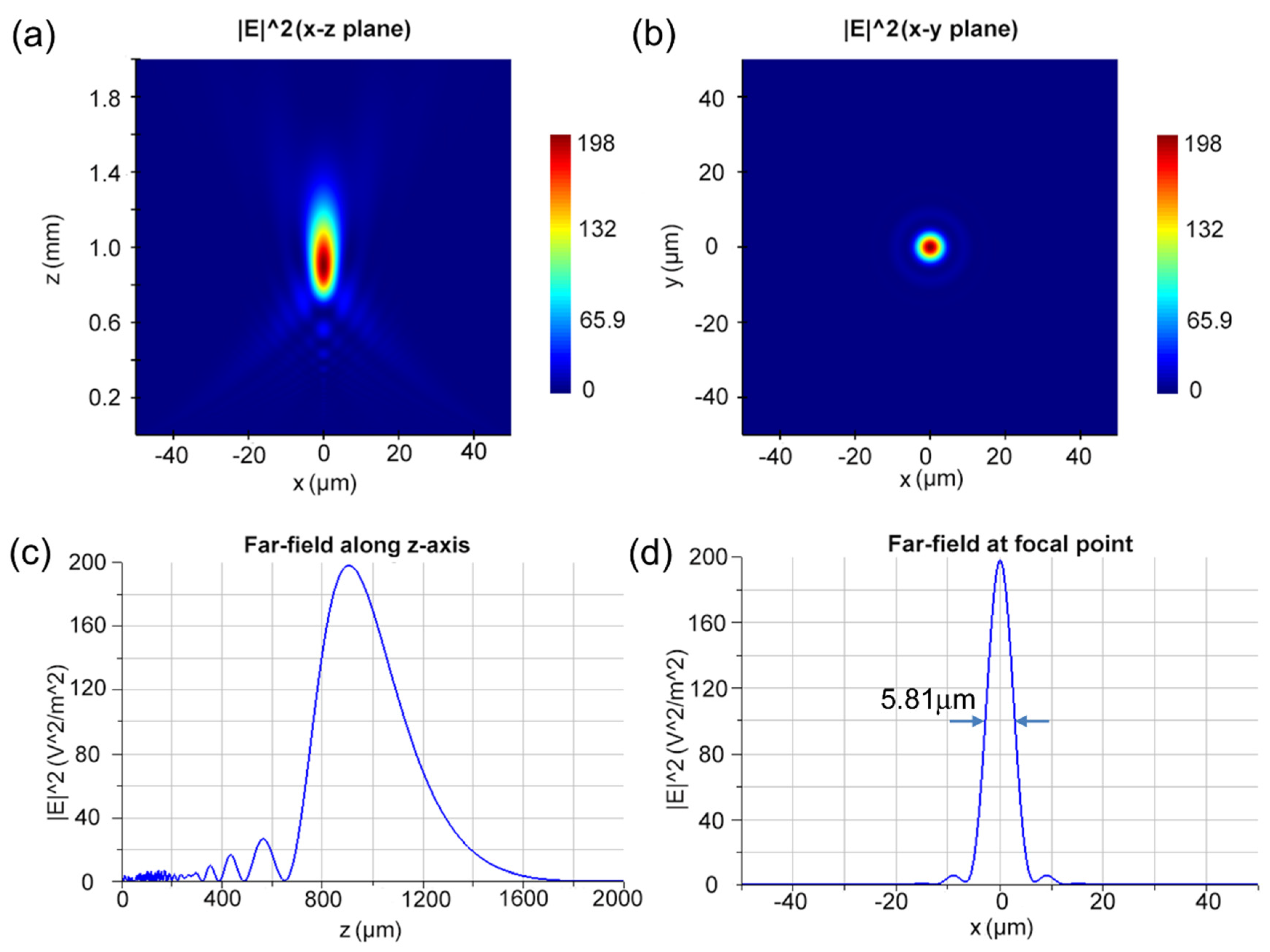
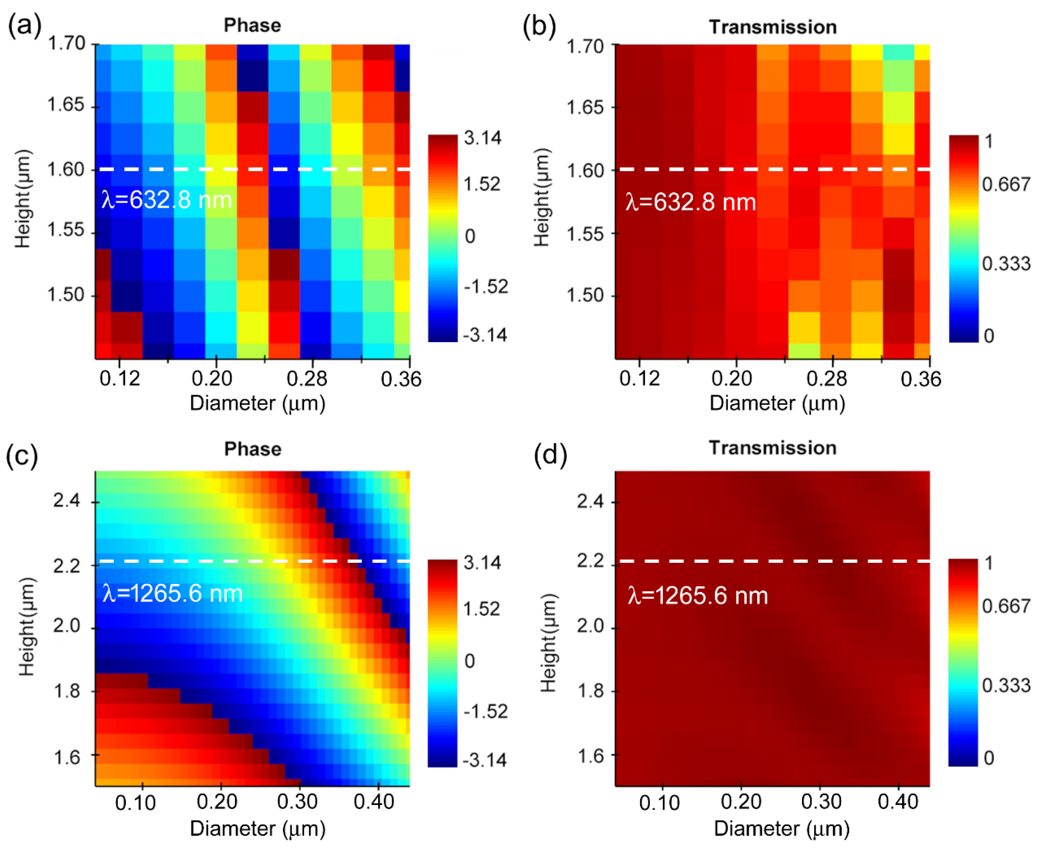
3.1. Dual-Wavelength Metalens with Small Aperture
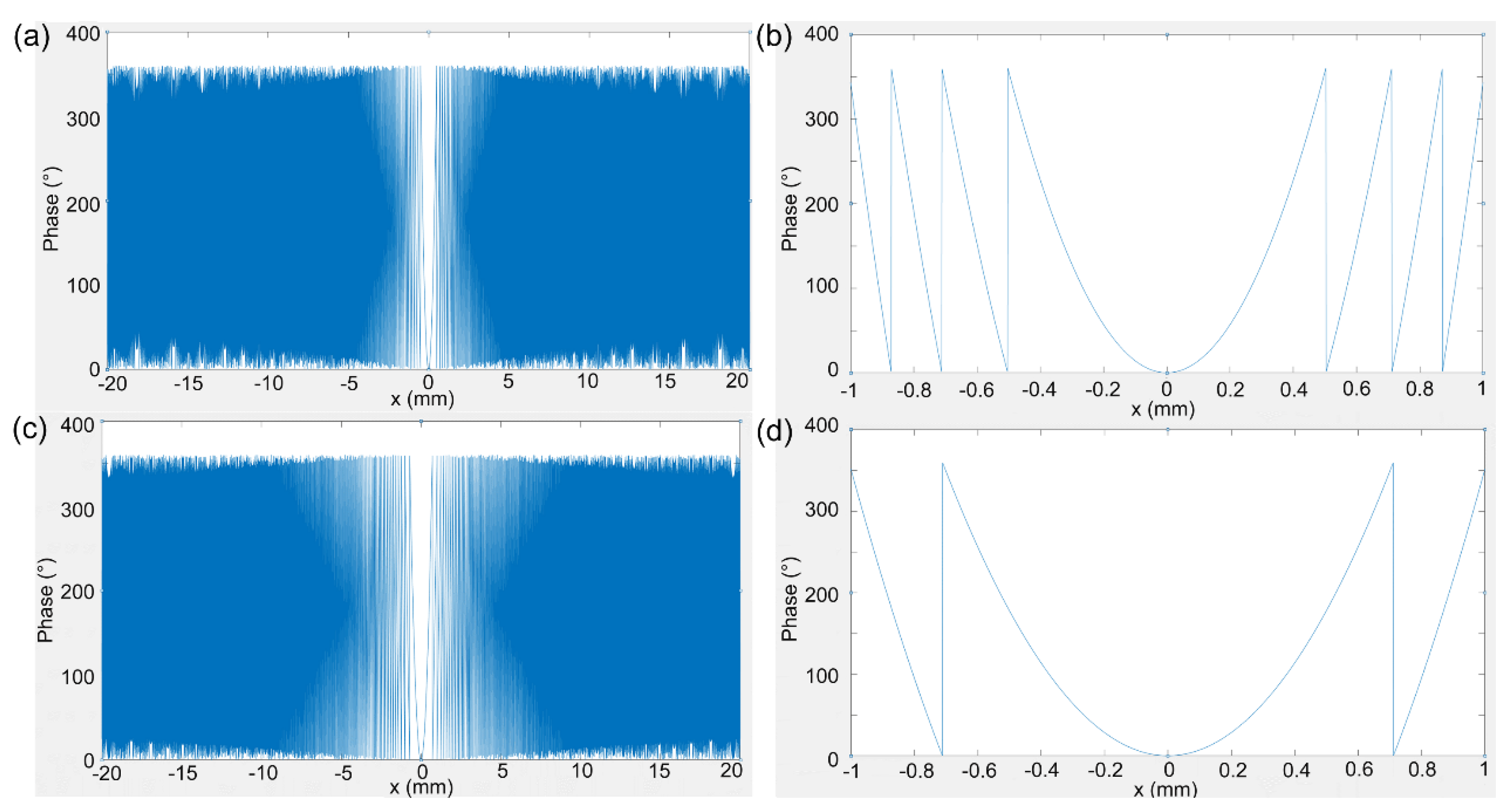
3.2. Dual-Wavelength Metalens with Large Aperture and Long Focal Length
4. Conclusions
Author Contributions
Funding
Data Availability Statement
Conflicts of Interest
References
- Luo, X.G.; Zhang, F.; Pu, M.B.; Guo, Y.H.; Li, X.; Ma, X.L. Recent advances of wide-angle metalenses: Principle, design, and applications. Nanophotonics 2021, 11, 1–20. [Google Scholar] [CrossRef]
- Zhang, L.D.; Chang, S.Y.; Chen, X.; Ding, Y.M.; Rahman, M.T.; Duan, Y.; Stephen, M.; Ni, X.J. High-Efficiency, 80 mm Aperture Metalens Telescope. Nano Lett. 2022, 23, 51–57. [Google Scholar] [CrossRef] [PubMed]
- Najarian, A.M.; Vafaie, M.; Johnston, A.; Zhu, T.; Wei, M.; Saidaminov, M.I.; Hou, Y.; Hoogland, S.; Arquer, F.P.G.; Sargent, E.H. Sub-millimetre light detection and ranging using perovskites. Nat. Electron. 2022, 5, 511–518. [Google Scholar] [CrossRef]
- Arbabi, A.; Faraon, A. Advances in optical metalenses. Nat. Photon. 2022, 17, 16–25. [Google Scholar] [CrossRef]
- Yu, N.; Genevet, P.; Kats, M.A.; Aieta, F.; Tetienne, J.; Capasso, F.; Gaburro, A.Z. Light propagation with phase discontinuities: Generalized laws of reflection and refraction. Science 2011, 334, 333–337. [Google Scholar] [CrossRef] [PubMed]
- Monticone, F.; Estakhri, N.; Alù, A. Full control of nanoscale optical transmission with a composite metascreen. Phys. Rev. Lett. 2013, 110, 203903. [Google Scholar] [CrossRef] [PubMed]
- Khorasaninejad, M.; Chen, W.T.; Devlin, R.C.; Oh, J.; Zhu, A.Y.; Capasso, F. Metalenses at visible wavelengths: Diffraction-limited focusing and subwavelength resolution imaging. Science 2016, 352, 1190–1194. [Google Scholar] [CrossRef] [PubMed]
- Decker, M.; Staude, I.; Falkner, M.; Dominguez, J.; Neshev, D.N.; Brener, I.; Pertsch, T.; Kivshar, Y.S. High-efficiency dielectric Huygens’ surfaces. Adv. Opt. Mater. 2015, 3, 813–820. [Google Scholar] [CrossRef]
- Khorasaninejad, M.; Capasso, F. Metalenses: Versatile multifunctional photonic components. Science 2017, 358, eaam8100. [Google Scholar] [CrossRef]
- Lu, D.; Liu, Z. Hyperlenses and metalenses for far-field super-resolution imaging. Nat. Commun. 2012, 3, 1205. [Google Scholar] [CrossRef]
- Zou, X.J.; Zheng, G.; Yuan, Q.; Zang, W.B.; Chen, R.; Li, T.Y.; Li, L.; Wang, S.M.; Wang, Z.L.; Zhu, S.N. Imaging based on metalenses. PhotoniX 2020, 1, 2. [Google Scholar] [CrossRef]
- Zhou, Y.; Zheng, H.; Kravchenko, I.I.; Valentine, J. Flat optics for image differentiation. Nat. Photon. 2020, 14, 316–323. [Google Scholar] [CrossRef]
- Yuan, Y.; Yan, Z.L.; Zhang, P.F.; Chang, Z.; Peng, F.J.; Chen, R.T.; Yang, Z.Y.; Chen, S.Z.; Zhao, Q.; Huang, X.P. A broadband achromatic dielectric planar metalens in mid-IR range. Photon. Sens. 2022, 13, 230126. [Google Scholar] [CrossRef]
- Tseng, M.L.; Hsiao, H.H.; Chu, C.H.; Chen, M.K.; Sun, G.; Liu, A.Q.; Tsai, D.P. Metalenses: Advances and applications. Adv. Opt. Mater. 2018, 6, 1800554. [Google Scholar] [CrossRef]
- Arbabi, A.; Horie, Y.; Bagheri, M.; Faraon, A. Dielectric metasurfaces for complete control of phase and polarization with subwavelength spatial resolution and high transmission. Nat. Nanotechnol. 2015, 10, 937–943. [Google Scholar] [CrossRef]
- Kamali, S.M.; Arbabi, E.; Arbabi, A.; Faraon, A. A review of dielectric optical metasurfaces for wavefront control. Nanophotonics 2018, 7, 1041–1068. [Google Scholar] [CrossRef]
- Pan, M.; Fu, Y.F.; Zheng, M.J.; Chen, H.; Zang, Y.J.; Duan, H.G.; Li, Q.; Qiu, M.; Hu, Y.Q. Dielectric metalens for miniaturized imaging systems: Progress and challenges. Light Sci. Appl. 2022, 11, 195. [Google Scholar] [CrossRef] [PubMed]
- Kim, S.J.; Kim, C.Y.; Kim, Y.J.; Jeong, J.; Choi, S.; Han, W.; Kim, J.; Lee, B. Dielectric metalens: Properties and three-dimensional imaging applications. Sensors 2021, 21, 4584. [Google Scholar] [CrossRef]
- Gigli, C.; Li, Q.T.; Chavel, P.; Leo, G.; Brongersma, M.L.; Lalanne, P. Fundamental limitations of Huygens’ metasurfaces for optical beam shaping. Laser Photon. Rev. 2021, 15, 2000448. [Google Scholar] [CrossRef]
- Arbabi, A.; Faraon, A. Fundamental limits of ultrathin metasurfaces. Sci. Rep. 2017, 7, srep43722. [Google Scholar] [CrossRef]
- Fu, B.Y.; Li, T.Y.; Zou, X.J.; Ren, J.Z.; Yuan, Q.; Wang, S.M.; Cao, X.; Wang, Z.L.; Zhu, S.N. Steerable chromatic dispersive metalenses in dual bands. J. Phys. D 2022, 55, 25510. [Google Scholar] [CrossRef]
- Fan, Y.B.; Yao, J.; Tsai, D.P. Advance of large-area achromatic flat lenses. Light Sci. Appl. 2023, 12, 51. [Google Scholar] [CrossRef] [PubMed]
- Wang, S.; Wu, P.C.; Su, V.C.; Lai, Y.C.; Chen, M.K.; Kuo, H.Y.; Chen, B.H.; Chen, Y.H.; Huang, T.T.; Wang, J.H.; et al. A broadband achromatic metalens in the visible. Nat. Nanotechnol. 2018, 13, 227–232. [Google Scholar] [CrossRef]
- Wang, Y.J.; Chen, Q.M.; Yang, W.H.; Ji, Z.H.; Jin, L.M.; Ma, X.; Song, Q.H.; Boltasseva, A.; Han, J.; Shalaev, V.M.; et al. High-efficiency broadband achromatic metalens for near-IR biological imaging window. Nat. Commun. 2021, 12, 5560. [Google Scholar] [CrossRef] [PubMed]
- Aieta, F.; Kats, M.A.; Genevet, P.; Capasso, F. Multiwavelength achromatic metasurfaces by dispersive phase compensation. Science 2015, 347, 1342–1345. [Google Scholar] [CrossRef]
- Arbabi, E.; Arbabi, A.; Kamali, S.M.; Horie, Y.; Faraon, A. Multiwavelength metasurfaces through spatial multiplexing. Sci. Rep. 2016, 6, 32803. [Google Scholar] [CrossRef]
- Avayu, O.; Almeida, E.; Prior, Y.; Ellenbogen, T. Composite functional metasurfaces for multispectral achromatic optics. Nat. Commun. 2017, 8, 14992. [Google Scholar] [CrossRef] [PubMed]
- Shrestha, S.; Overvig, A.C.; Lu, M.; Stein, A.; Yu, N. Broadband achromatic dielectric metalenses. Light Sci. Appl. 2018, 7, 85. [Google Scholar] [CrossRef]
- Chen, W.T.; Zhu, A.Y.; Sanjeev, V.; Khorasaninejad, M.; Shi, Z.J.; Lee, E.; Chen, F.C. A broadband achromatic metalens for focusing and imaging in the visible. Nat. Nanotechnol. 2018, 13, 220–226. [Google Scholar] [CrossRef]
- Chen, W.T.; Zhu, A.Y.; Capasso, F. Flat optics with dispersion-engineered metasurfaces. Nat. Rev. Mater. 2020, 5, 604–620. [Google Scholar] [CrossRef]
- Presutti, F.; Monticone, F. Focusing on bandwidth: Achromatic metalens limits. Optica 2020, 7, 624–631. [Google Scholar] [CrossRef]
- Zhang, H.B.; Du, J.S.; Chi, Z.T.; Cong, H.L.; Wang, B. Numerical design of a dual-wavelength confocal metalens with photonic crystal filter based on filter-substrate-metasurface structure. Opt. Commun. 2024, 554, 130157. [Google Scholar] [CrossRef]
- Wang, S.; Wu, P.C.; Su, V.-C.; Lai, Y.-C.; Chu, C.H.; Chen, J.-W.; Lu, S.-H.; Chen, J.; Xu, B.; Kuan, C.-H.; et al. Broadband achromatic optical metasurface devices. Nat. Commun. 2017, 8, 187. [Google Scholar] [CrossRef] [PubMed]
- Xiao, X.J.; Zhao, Y.W.; Ye, X.; Chen, C.; Lu, X.M.; Rong, Y.S.; Deng, J.H.; Li, G.X.; Zhu, S.N.; Li, T. Large-scale achromatic flat lens by light frequency-domain coherence optimization. Light Sci. Appl. 2022, 11, 323. [Google Scholar] [CrossRef] [PubMed]
- Liu, X.; Deng, J.H.; Li, K.F.; Jin, M.K.; Tang, Y.; Zhang, X.C.; Cheng, X.; Wang, H.; Liu, W.; Li, G.X. Optical telescope with Cassegrain metasurfaces. Nanophotonics 2020, 9, 3263–3269. [Google Scholar] [CrossRef]
- Cunningham, C. Future optical technologies for telescopes. Nat. Photon. 2009, 3, 239–241. [Google Scholar] [CrossRef]
- She, A.; Zhang, S.Y.; Shian, S.; Clarke, D.R.; Capasso, F. Large area metalenses: Design, characterization, and mass manufacturing. Opt. Express 2018, 26, 1573–1585. [Google Scholar] [CrossRef]
- Hamed, A.M. Improvement of Point Spread Function (PSF) using linear-quadratic aperture. Optik 2017, 131, 838–849. [Google Scholar] [CrossRef]


Disclaimer/Publisher’s Note: The statements, opinions and data contained in all publications are solely those of the individual author(s) and contributor(s) and not of MDPI and/or the editor(s). MDPI and/or the editor(s) disclaim responsibility for any injury to people or property resulting from any ideas, methods, instructions or products referred to in the content. |
© 2024 by the authors. Licensee MDPI, Basel, Switzerland. This article is an open access article distributed under the terms and conditions of the Creative Commons Attribution (CC BY) license (https://creativecommons.org/licenses/by/4.0/).
Share and Cite
Guo, C.; Zheng, Z.; Liu, Z.; Yan, Z.; Wang, Y.; Chen, R.; Liu, Z.; Yu, P.; Wan, W.; Zhao, Q.; et al. Design and Analysis of the Dual-Band Far-Field Super-Resolution Metalens with Large Aperture. Nanomaterials 2024, 14, 513. https://doi.org/10.3390/nano14060513
Guo C, Zheng Z, Liu Z, Yan Z, Wang Y, Chen R, Liu Z, Yu P, Wan W, Zhao Q, et al. Design and Analysis of the Dual-Band Far-Field Super-Resolution Metalens with Large Aperture. Nanomaterials. 2024; 14(6):513. https://doi.org/10.3390/nano14060513
Chicago/Turabian StyleGuo, Cheng, Zhishuai Zheng, Ziang Liu, Zilong Yan, Yucheng Wang, Ruotong Chen, Zhuonan Liu, Peiquan Yu, Weihao Wan, Qing Zhao, and et al. 2024. "Design and Analysis of the Dual-Band Far-Field Super-Resolution Metalens with Large Aperture" Nanomaterials 14, no. 6: 513. https://doi.org/10.3390/nano14060513
APA StyleGuo, C., Zheng, Z., Liu, Z., Yan, Z., Wang, Y., Chen, R., Liu, Z., Yu, P., Wan, W., Zhao, Q., & Huang, X. (2024). Design and Analysis of the Dual-Band Far-Field Super-Resolution Metalens with Large Aperture. Nanomaterials, 14(6), 513. https://doi.org/10.3390/nano14060513