
Study of Electrical and Dielectric Behaviors of Copper-Doped Zinc Oxide Ceramic Prepared by Spark Plasma Sintering for Electronic Device Applications

 ,
,  ,
,  ,
,  ,
,  and
and 
Abstract
1. Introduction
2. Materials and Methods
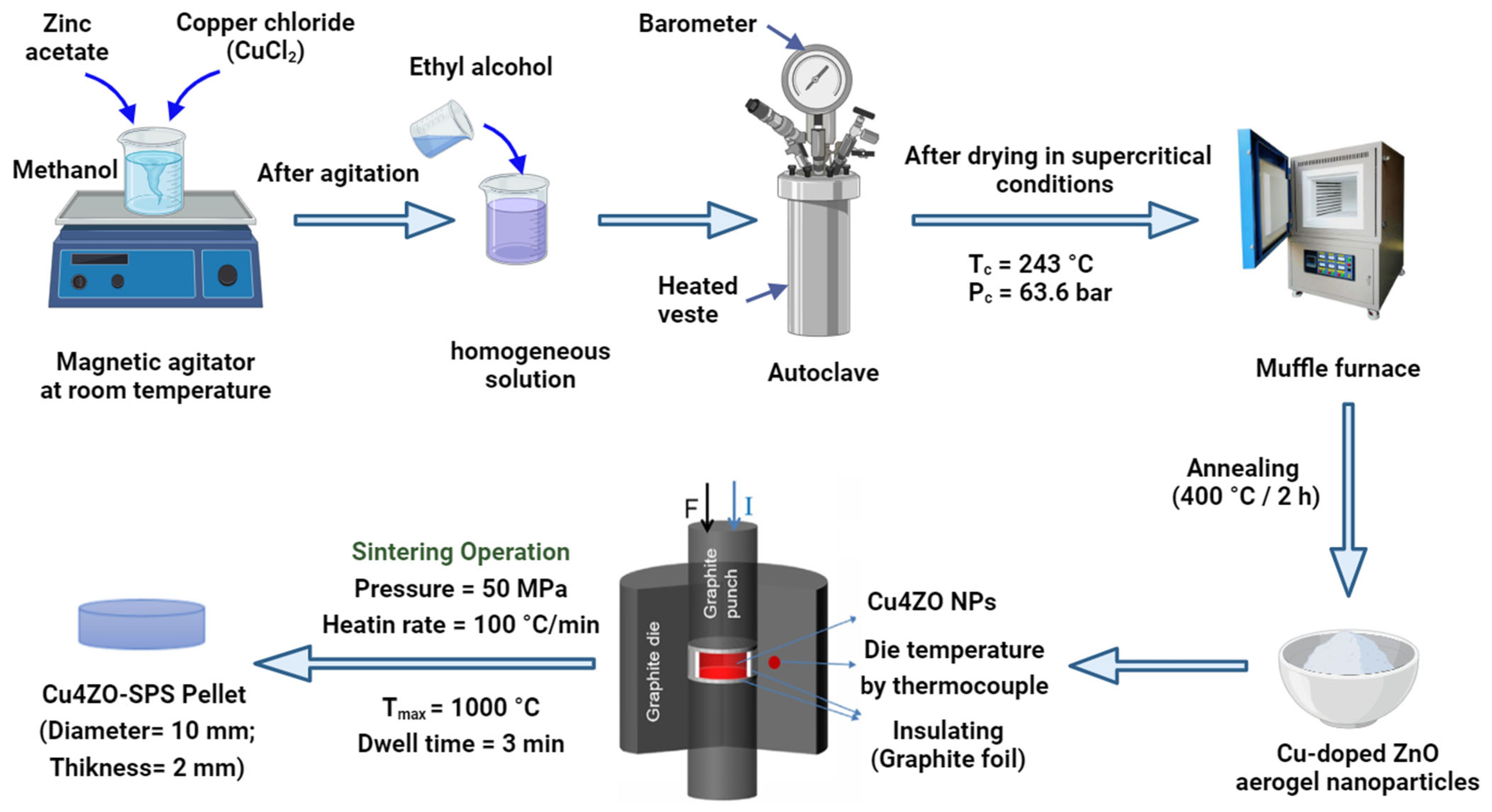
2.1. Cu-Doped ZnO Nanoparticle Preparation
2.2. Cu-Doped ZnO Ceramic Preparation by Spark Plasma Sintering
2.3. Characterizations
3. Results and Discussion
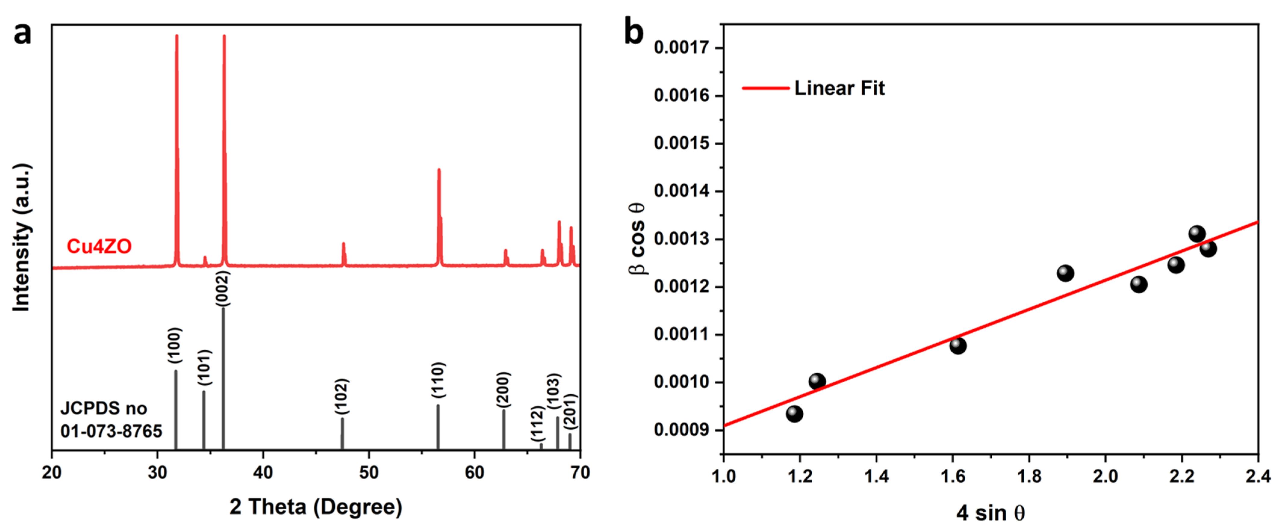
3.1. Structural Properties
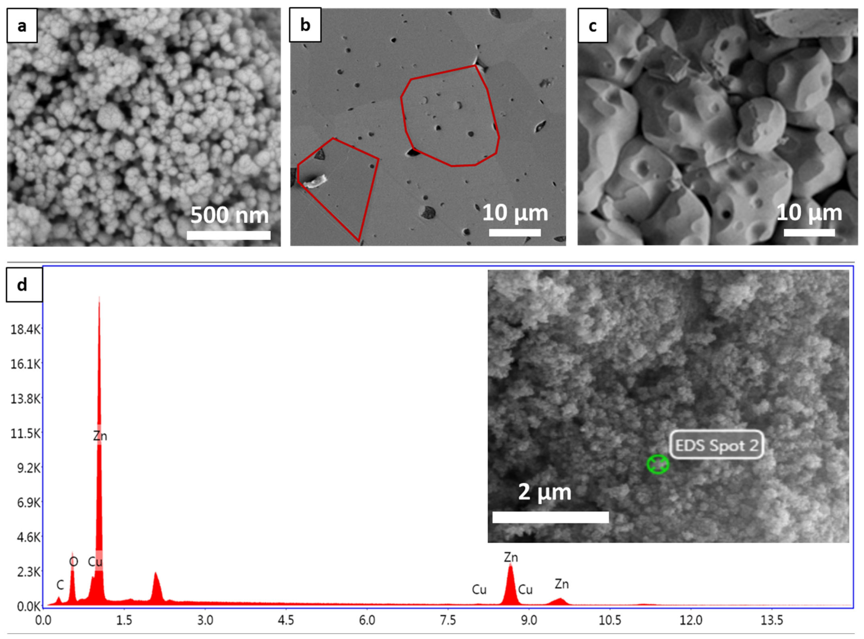
3.2. Morphological and Chemical Composition Properties
3.3. Electrical Behaviors
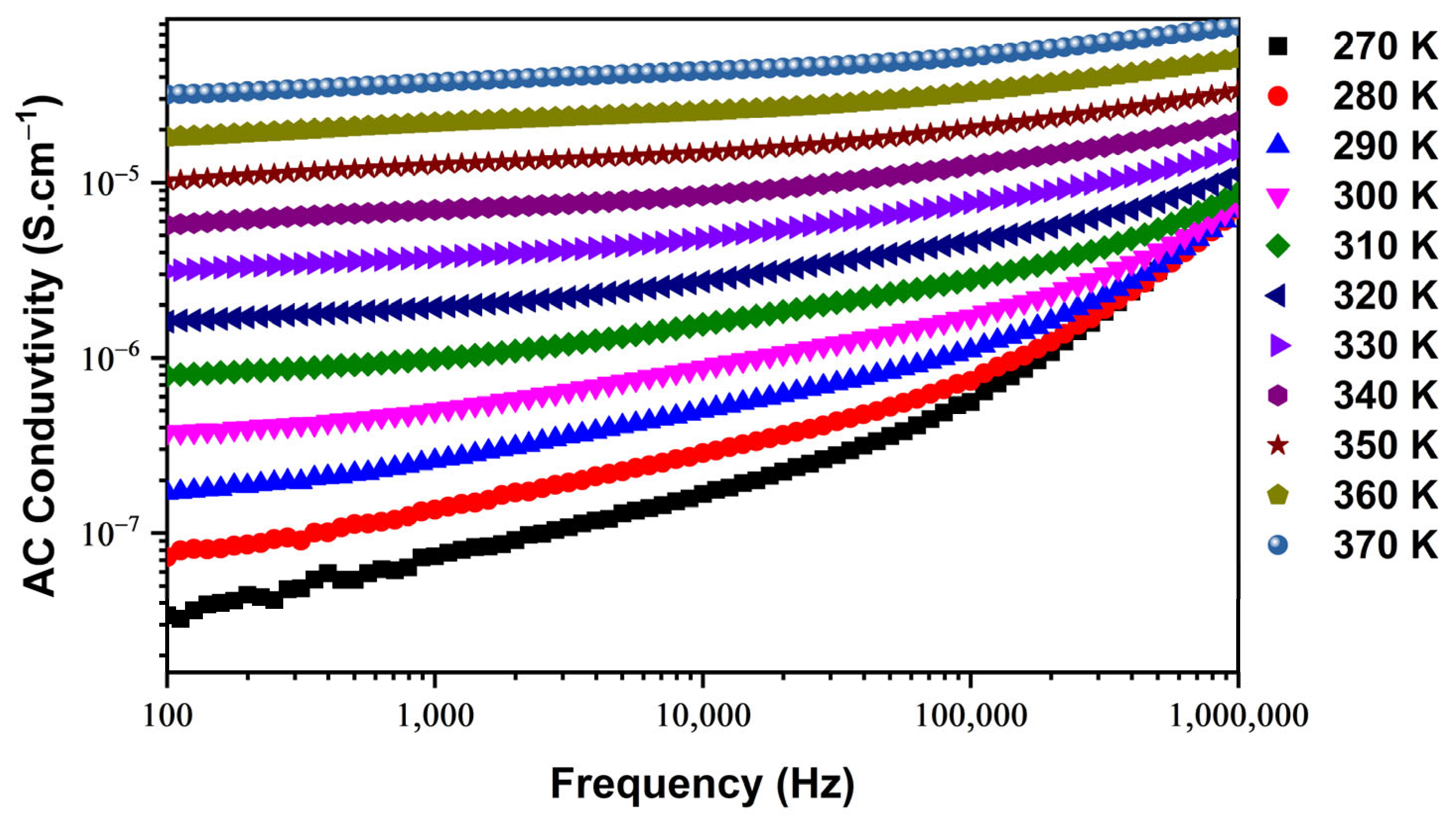
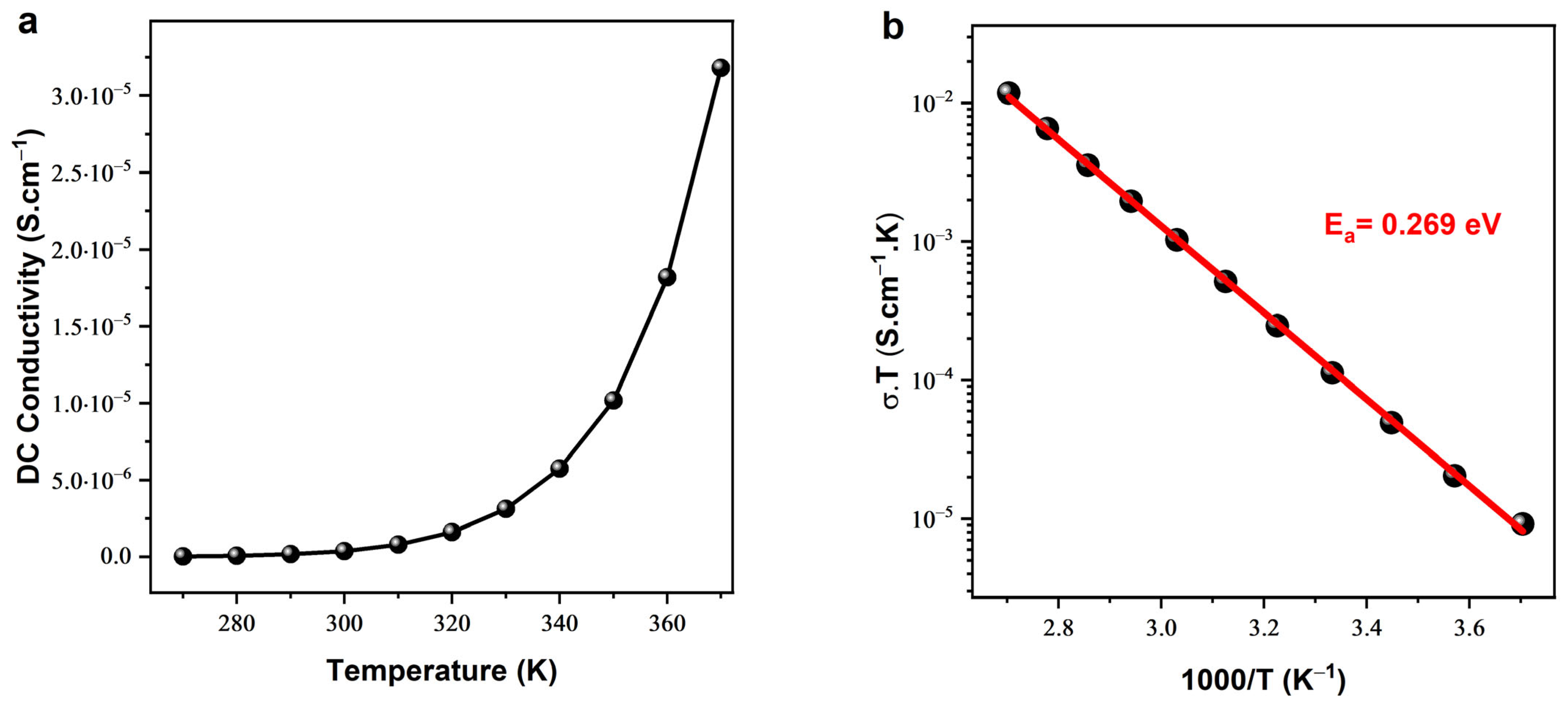
3.3.1. Electrical Conductivity
3.3.2. Electrical Impedance
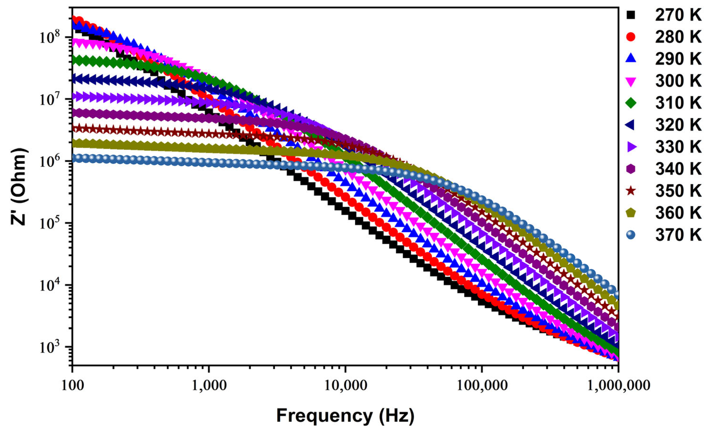
Real Part of Impedance
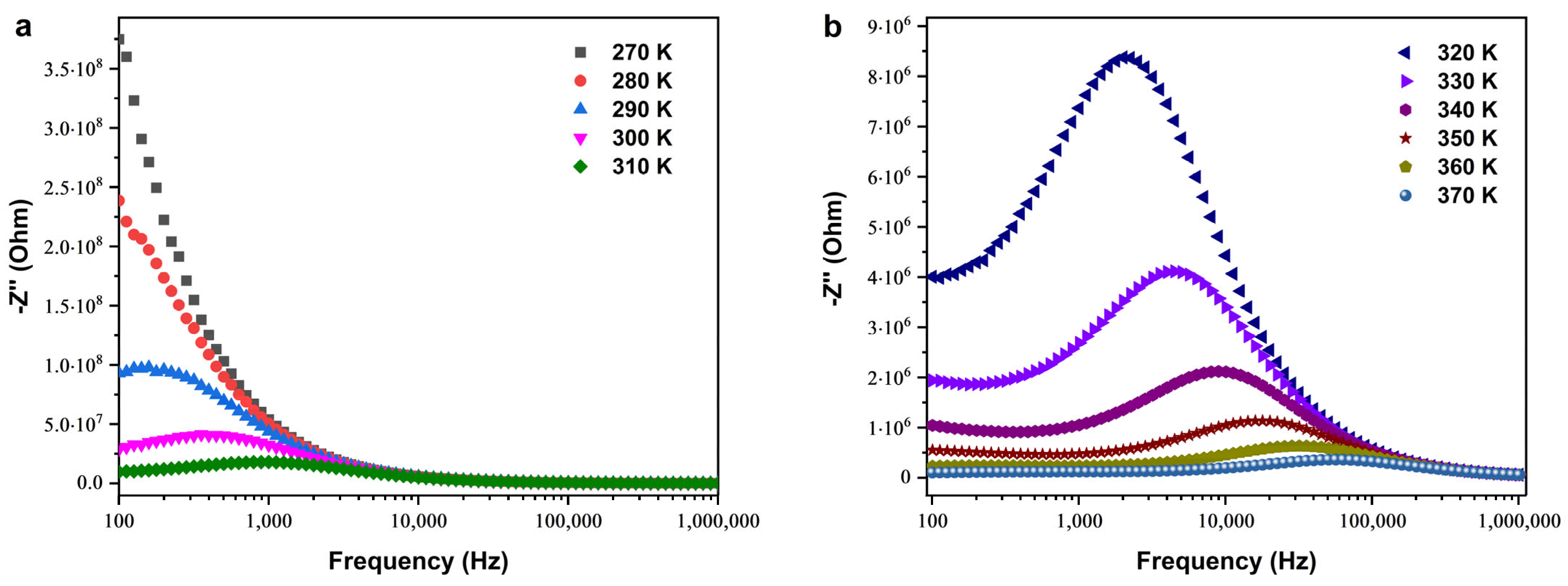
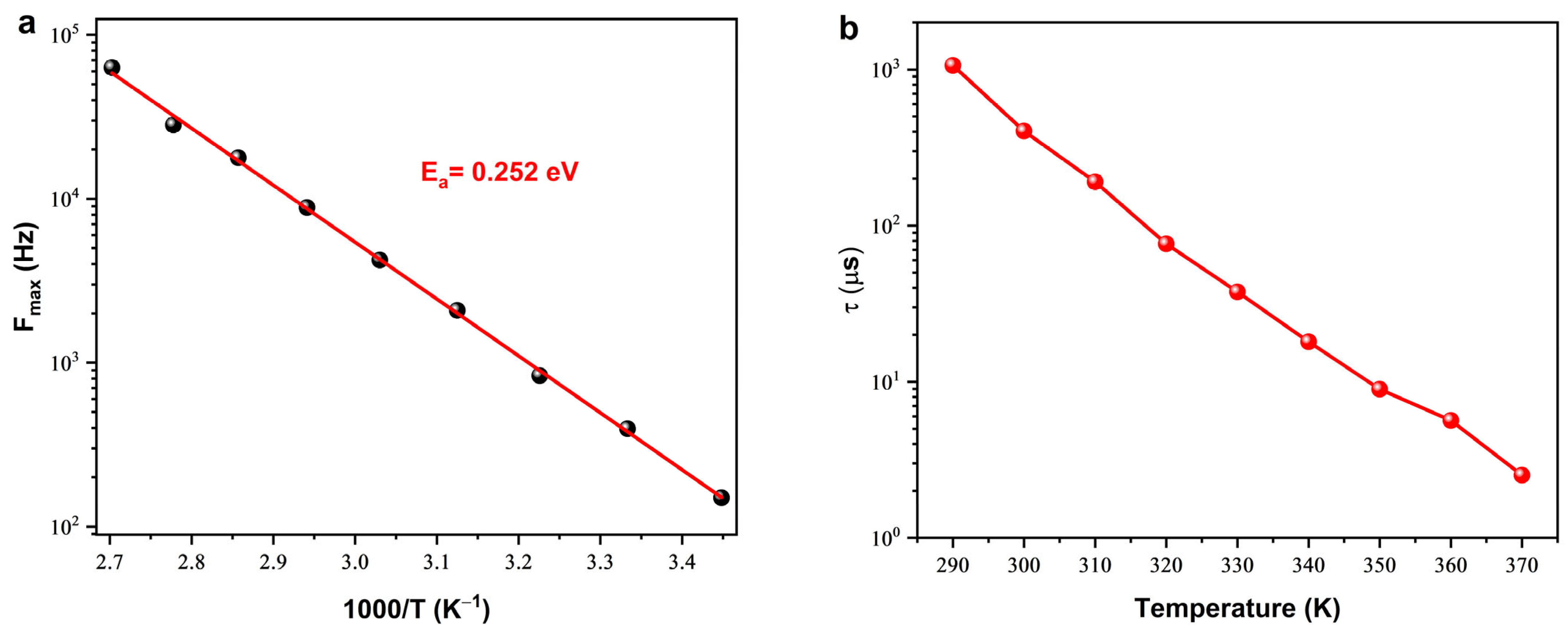
Imaginary Part of Impedance
Nyquist Diagrams
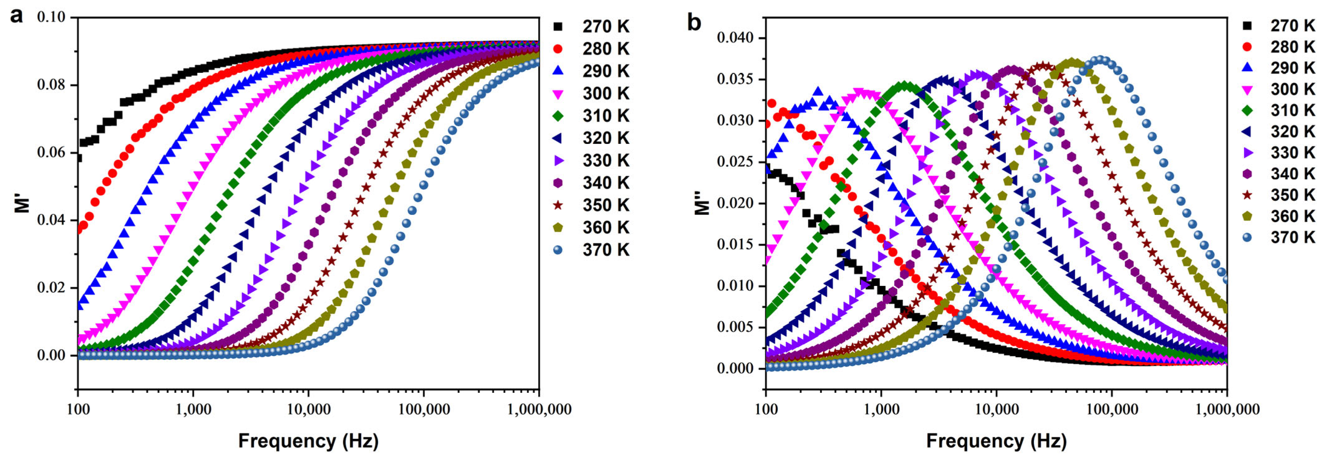
Electrical Modulus
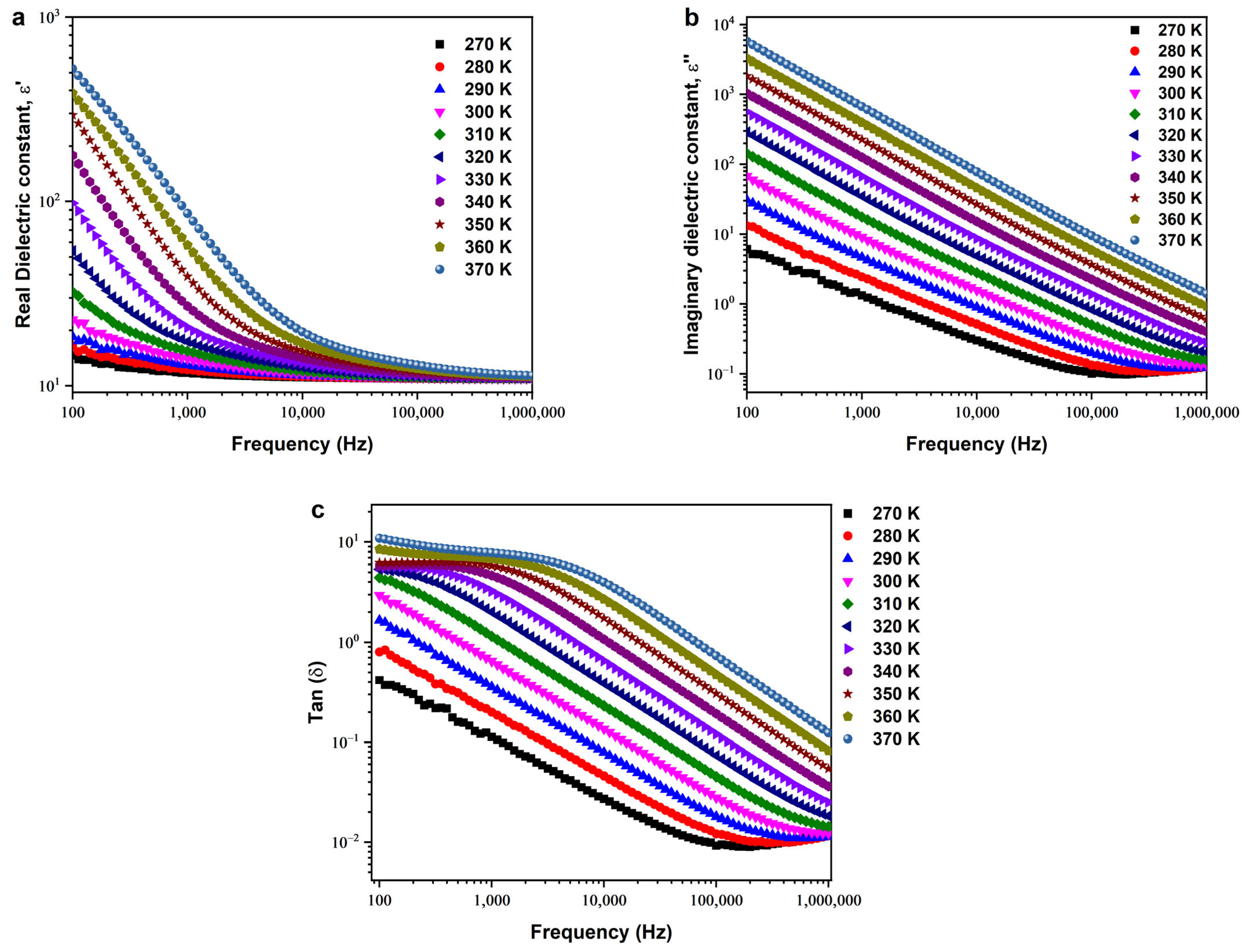
3.4. Dielectric Behaviors
4. Conclusions
Author Contributions
Funding
Data Availability Statement
Acknowledgments
Conflicts of Interest
References
- Viet Vu, D.; Hai Le, D.; Xuan Nguyen, C.; Quang Trinh, T. Comparison of structural and electric properties of ZnO-based n-type thin films with different dopants for thermoelectric applications. J. Sol-Gel Sci. Technol. 2019, 91, 146–153. [Google Scholar] [CrossRef]
- Mohammed, M.A.; Sudin, I.; Noor, A.M.; Rajoo, S.; Uday, M.B.; Obayes, N.H.; Omar, M.F. A review of thermoelectric ZnO nanostructured ceramics for energy recovery. Int. J. Eng. Technol. 2018, 7, 27–30. [Google Scholar] [CrossRef]
- Pascariu, P.; Homocianu, M. ZnO-based ceramic nanofibers: Preparation, properties and applications. Ceram. Int. 2019, 45, 11158–11173. [Google Scholar] [CrossRef]
- Singhal, S.; Kaur, J.; Namgyal, T.; Sharma, R. Cu-doped ZnO nanoparticles: Synthesis, structural and electrical properties. Phys. B Condens. Matter 2012, 407, 1223–1226. [Google Scholar] [CrossRef]
- Maldonado, F.; Stashans, A. Al-doped ZnO: Electronic, electrical and structural properties. J. Phys. Chem. Solids 2010, 71, 784–787. [Google Scholar] [CrossRef]
- Bhosle, V.; Tiwari, A.; Narayan, J. Electrical properties of transparent and conducting Ga doped ZnO. J. Appl. Phys. 2006, 100, 033713. [Google Scholar] [CrossRef]
- Chen, K.J.; Hung, F.Y.; Chang, S.J.; Hu, Z.S. Microstructures, optical and electrical properties of In-doped ZnO thin films prepared by sol–gel method. Appl. Surf. Sci. 2009, 255, 6308–6312. [Google Scholar] [CrossRef]
- Omri, K.; Bettaibi, A.; Khirouni, K.; El Mir, L. The optoelectronic properties and role of Cu concentration on the structural and electrical properties of Cu doped ZnO nanoparticles. Phys. B Condens. Matter 2018, 537, 167–175. [Google Scholar] [CrossRef]
- Elilarassi, R.; Chandrasekaran, G. Structural, optical and magnetic characterization of Cu-doped ZnO nanoparticles synthesized using solid state reaction method. J. Mater. Sci. Mater. Electron. 2009, 21, 1168–1173. [Google Scholar] [CrossRef]
- Palmero, P. Structural ceramic nanocomposites: A review of properties and powders’ synthesis methods. Nanomaterials 2015, 5, 656–696. [Google Scholar] [CrossRef]
- Radingoana, P.M.; Guillemet-Fritsch, S.; Noudem, J.; Olubambi, P.A.; Chevallier, G.; Estournès, C. Microstructure and thermoelectric properties of Al-doped ZnO ceramic prepared by spark plasma sintering. J. Eur. Ceram. Soc. 2023, 43, 1009–1016. [Google Scholar] [CrossRef]
- Sulaiman, S.; Izman, S.; Uday, M.B.; Omar, M.F. Review on grain size effects on thermal conductivity in ZnO thermoelectric materials. RSC Adv. 2022, 12, 5428–5438. [Google Scholar] [CrossRef] [PubMed]
- Zhao, X.; Xiao, Y.; Kang, S.; Li, Y.; Cheng, L.; Ren, C.; Guo, J.; Wang, X.; Yang, L.; Liao, R. Comparative study on energy efficiency and densification of ZnO ceramics using various sintering processes. J. Mater. Sci. Mater. Electron. 2023, 34, 1798. [Google Scholar] [CrossRef]
- Liang, J.; Zhao, X.; Kang, S.; Guo, J.; Chen, Z.; Long, Y.; Zeng, Q.; Sun, J.; Yang, L.; Liao, R.; et al. Microstructural evolution of ZnO via hybrid cold sintering/spark plasma sintering. J. Eur. Ceram. Soc. 2022, 42, 5738–5746. [Google Scholar] [CrossRef]
- Bandyopadhyay, P.; Dey, A.; Basu, R.; Das, S.; Nandy, P. Synthesis and characterization of copper doped zinc oxide nanoparticles and its application in energy conversion. Curr. Appl. Phys. 2014, 14, 1149–1155. [Google Scholar] [CrossRef]
- Hadia, N.M.A.; Aljudai, M.; Alzaid, M.; Mohamed, S.H.; Mohamed, W.S. Synthesis and characterization of undoped and copper-doped zinc oxide nanowires for optoelectronic and solar cells applications. Appl. Phys. A 2021, 128, 17. [Google Scholar] [CrossRef]
- Kharchouche, F.; Belkhiat, S. Effect of spark plasma sintering on microstructure and electrical properties of ZnO-based varistors. J. Mater. Sci. Mater. Electron. 2018, 29, 16238–16247. [Google Scholar] [CrossRef]
- Kougo, T.; Yoshikawa, A. Fabrication and characterization of polycrystalline bulk ZnO with large grain size of ~100 μm by the spark plasma sintering. Phys. Status Solidi C 2006, 3, 785–788. [Google Scholar] [CrossRef]
- Arias-Serrano, B.I.; Mikhalev, S.M.; Ferro, M.C.; Tobaldi, D.M.; Frade, J.R.; Kovalevsky, A.V. On the high-temperature degradation mechanism of ZnO-based thermoelectrics. J. Eur. Ceram. Soc. 2021, 41, 1730–1734. [Google Scholar] [CrossRef]
- Liu, B.; Abbas, A.; Zhou, C. Two-dimensional semiconductors: From materials preparation to electronic applications. Adv. Electron. Mater. 2017, 3, 1700045. [Google Scholar] [CrossRef]
- Hassan, K.; Chung, G.-S. Catalytically activated quantum-size Pt/Pd bimetallic core–shell nanoparticles decorated on ZnO nanorod clusters for accelerated hydrogen gas detection. Sens. Actuators B Chem. 2017, 239, 824–833. [Google Scholar] [CrossRef]
- Williamson, G.K.; Hall, W.H. X-ray Line Broadening from Filed Aluminium and Wolfram. Acta Metall. 1953, 1, 22–31. [Google Scholar] [CrossRef]
- Chen, Z.; Shan, Z.; Cao, M.S.; Lu, L.; Mao, S.X. Zinc oxide nanotetrapods. Nanotechnology 2004, 15, 365–369. [Google Scholar] [CrossRef]
- Khassaf, H.; Yadavalli, S.K.; Zhou, Y.; Padture, N.P.; Kingon, A.I. Effect of grain boundaries on charge transport in methylammonium lead iodide perovskite thin films. J. Phys. Chem. C 2019, 123, 5321–5325. [Google Scholar] [CrossRef]
- Moreira, R.; dos Santos, L.P.; Salomão, C.; Barros, E.B.; Vasconcelos, I.F. Influence of Grain Boundaries on Nanoscale Charge Transport Properties of Transparent Conductive ZnO-Based Electrodes. ACS Appl. Electron. Mater. 2023, 6, 415–425. [Google Scholar] [CrossRef]
- Benamara, M.; Bouzidi, S.; Zahmouli, N.; Teixeira, S.S.; Graça, M.P.F.; El Mir, L.; Valente, M.A. Electrical transport of Mg-doped maghemite (γ-Fe2O3) nanoparticles. Appl. Phys. A 2022, 128, 624. [Google Scholar] [CrossRef]
- Belkhaoui, C.; Lefi, R.; Mzabi, N.; Smaoui, H. Synthesis, optical and electrical properties of Mn doped ZnO nanoparticles. J. Mater. Sci. Mater. Electron. 2018, 29, 7020–7031. [Google Scholar] [CrossRef]
- Tayari, F.; Nassar, K.I.; Benamara, M.; Essid, M.; Teixeira, S.S.; Graça, M.F. Sol–gel synthesized (Bi0.5Ba0.5Ag)0.5(NiMn)0.5O3 perovskite ceramic: An exploration of its structural characteristics, dielectric properties and electrical conductivity. Ceram. Int. 2024, in press. [Google Scholar] [CrossRef]
- Kim, C.O.; Kim, S.; Oh, H.T.; Choi, S.-H.; Shon, Y.; Lee, S.; Na Hwang, H.; Hwang, C.-C. Effect of electrical conduction properties on magnetic behaviors of Cu-doped ZnO thin films. Phys. B Condens. Matter 2010, 405, 4678–4681. [Google Scholar] [CrossRef]
- Wei, J.; Zhang, Q.; Zhao, L.; Hao, L.; Yang, C. Enhanced thermoelectric properties of carbon fiber reinforced cement composites. Ceram. Int. 2016, 42, 11568–11573. [Google Scholar] [CrossRef]
- Pradhan, S.S.; Unnikrishnan, L.; Mohanty, S.; Nayak, S.K. Thermally conducting polymer composites with EMI shielding: A review. J. Electron. Mater. 2020, 49, 1749–1764. [Google Scholar] [CrossRef]
- Kaner, R.B.; MacDiarmid, A.G. Plastics that Conduct Electricity. Sci. Am. 1988, 258, 106–111. [Google Scholar] [CrossRef]
- Nassar, K.I.; Tayari, F.; Benamara, M.; Teixeira, S.S.; Graça, M.P.F. Exploring bismuth-doped polycrystalline ceramic Ba0.75Bi0.25Ni0.7Mn0.3O3: Synthesis, structure, and electrical properties for advanced electronic applications. RSC Adv. 2023, 13, 24023–24030. [Google Scholar] [CrossRef] [PubMed]
- Sekrafi, H.E.; Kharrat, A.B.J.; Wederni, M.A.; Chniba-Boudjada, N.; Khirouni, K.; Boujelben, W. Impact of low titanium concentration on the structural, electrical and dielectric properties of Pr0.75Bi0.05Sr0.1Ba0.1Mn1−xTixO3 (x = 0, 0.04) compounds. J. Mater. Sci. Mater. Electron. 2018, 30, 876–891. [Google Scholar] [CrossRef]
- Sekrafi, H.; Kharrat, A.B.J.; Wederni, M.; Khirouni, K.; Chniba-Boudjada, N.; Boujelben, W. Structural, electrical, dielectric properties and conduction mechanism of sol-gel prepared Pr0.75Bi0.05Sr0.1Ba0.1Mn0.98Ti0.02O3 compound. Mater. Res. Bull. 2018, 111, 329–337. [Google Scholar] [CrossRef]
- Guettiti, K.; Sekrafi, H.E.; Azizi, S.; Bouzidi, C.; Bouguila, N.; Khirouni, K.; Lamloumi, J. The study of structural, dielectric, impedance and modulus properties of La0.8Pb0.2FeO3 doped by 25% Mg into the B-site. Phys. B Condens. Matter 2023, 655, 414771. [Google Scholar] [CrossRef]
- Wang, S.; Zhang, J.; Gharbi, O.; Vivier, V.; Gao, M.; Orazem, M.E. Electrochemical impedance spectroscopy. Nat. Rev. Methods Primers. 2021, 1, 41. [Google Scholar] [CrossRef]
- Nassar, K.I.; Benamara, M.; Kechiche, L.; Teixeira, S.S.; Graça, M.P.F. Structural, electrical properties of bismuth and niobium-doped LaNiO3 perovskite obtained by sol–gel route for future electronic device applications. Indian J. Phys. 2024, 1–9. [Google Scholar] [CrossRef]
- Yu, L.; Cebe, P. Effect of nanoclay on relaxation of poly (vinylidene fluoride) nano-composites. J. Polym. Sci. Part B Polym. Phys. 2009, 47, 2520–2532. [Google Scholar] [CrossRef]
- Yang, F.; Li, L.; Wu, P.; Pradal-Velázquez, E.; Pearce, H.K.; Sinclair, D.C. Use of the time constant related parameter f max to calculate the activation energy of bulk conduction in ferroelectrics. J. Mater. Chem. C 2018, 6, 9258–9268. [Google Scholar] [CrossRef]
- Tang, R.; Jiang, C.; Qian, W.; Jian, J.; Zhang, X.; Wang, H.; Yang, H. Dielectric relaxation, resonance and scaling behaviors in Sr3Co2Fe24O41 hexaferrite. Sci. Rep. 2015, 5, 13645. [Google Scholar] [CrossRef] [PubMed]
- Shi, J.; Zhang, H.; Li, Y.; Jasieniak, J.J.; Li, Y.; Wu, H.; Meng, Q. Identification of high-temperature exciton states and their phase-dependent trapping behavior in lead halide perovskites. Energy Environ. Sci. 2018, 11, 1460–1469. [Google Scholar] [CrossRef]
- Zhang, Y.; Yuan, J.; Zhao, L.; Wu, B.; Zhang, B.; Zhang, P.; Zhang, S.; Dong, C. Boosting exciton dissociation and charge transfer in P-doped 2D porous g-C3N4 for enhanced H2 production and molecular oxygen activation. Ceram. Int. 2021, 48, 4031–4046. [Google Scholar] [CrossRef]
- Pradhan, D.K.; Choudhary, R.N.P.; Samantaray, B.K. Studies of structural, thermal and electrical behavior of polymer nanocomposite electrolytes. Express Polym. Lett. 2008, 2, 630–638. [Google Scholar] [CrossRef]
- Javed, M.; Khan, A.A.; Khan, M.N.; Kazmi, J.; Mohamed, M.A. Investigation on Non-Debye type relaxation and polaronic conduction mechanism in ZnCr2O4 ternary spinel oxide. Mater. Sci. Eng. B 2021, 269, 115168. [Google Scholar] [CrossRef]
- Jakobsen, B.; Maggi, C.; Christensen, T.; Dyre, J.C. Investigation of the shear-mechanical and dielectric relaxation processes in two monoalcohols close to the glass transition. J. Chem. Phys. 2008, 129, 184502. [Google Scholar] [CrossRef]
- Javed, M.; Khan, A.A.; Khisro, S.N.; Majeed, A.; Kazmi, J.; Bilkees, R.; Hussain, M.; Mohamed, M.A. Charge conduction mechanism and non-debye type relaxation in LaCrO3 perovskite orthochromite. Mater. Chem. Phys. 2022, 290, 126522. [Google Scholar] [CrossRef]
- Feliu, S.; Galván, J.; Morcillo, M. The charge transfer reaction in Nyquist diagrams of painted steel. Corros. Sci. 1990, 30, 989–998. [Google Scholar] [CrossRef]
- Benamara, M.; Zahmouli, N.; Teixeira, S.S.; Graça, M.P.F.; Mir, L.E.; Valente, M.A. Electrical and magnetic studies of maghemite (γ-Fe2O3) prepared by the sol–gel route. J. Electron. Mater. 2022, 51, 2698–2707. [Google Scholar] [CrossRef]
- Sambasiva Rao, K.; Murali Krishna, P.; Madhava Prasad, D. Effect of simultaneous substitution of Li+ and Ti4+ in ceramics of Pb2KNb5O15 on structure, dielectric, modulus, impedance and conductivity properties. Phys. Status Solidi 2007, 244, 2267–2287. [Google Scholar] [CrossRef]
- Arora, M.; Arora, V.; Kaur, S.; Kaur, J.; Kumar, S.; Singh, A. Evidence of non-debye behavior of Pb0.76Sm0.24Ti0. 76Fe0.24O3 ceramics by complex impedance spectroscopy. Mater. Today Proc. 2023, 80, 1079–1085. [Google Scholar] [CrossRef]
- Mhamdi, A.; Mimouni, R.; Amlouk, A.; Amlouk, M.; Belgacem, S. Study of copper doping effects on structural, optical and electrical properties of sprayed ZnO thin films. J. Alloy. Compd. 2014, 610, 250–257. [Google Scholar] [CrossRef]
- Choudhary, P.; Saxena, P.; Yadav, A.; Rai, V.N.; Mishra, A. Synthesis and characterization of Cu-doped ZnCdO nanomaterials with improved dielectric and impedance properties for potential applications. Ionics 2019, 25, 4991–5001. [Google Scholar] [CrossRef]
- Ashokkumar, M.; Muthukumaran, S. Electrical, dielectric, photoluminescence and magnetic properties of ZnO nanoparticles co-doped with Co and Cu. J. Magn. Magn. Mater. 2015, 374, 61–66. [Google Scholar] [CrossRef]

Disclaimer/Publisher’s Note: The statements, opinions and data contained in all publications are solely those of the individual author(s) and contributor(s) and not of MDPI and/or the editor(s). MDPI and/or the editor(s) disclaim responsibility for any injury to people or property resulting from any ideas, methods, instructions or products referred to in the content. |
© 2024 by the authors. Licensee MDPI, Basel, Switzerland. This article is an open access article distributed under the terms and conditions of the Creative Commons Attribution (CC BY) license (https://creativecommons.org/licenses/by/4.0/).
Share and Cite
Benamara, M.; Iben Nassar, K.; Rivero-Antúnez, P.; Essid, M.; Soreto Teixeira, S.; Zhao, S.; Serrà, A.; Esquivias, L. Study of Electrical and Dielectric Behaviors of Copper-Doped Zinc Oxide Ceramic Prepared by Spark Plasma Sintering for Electronic Device Applications. Nanomaterials 2024, 14, 402. https://doi.org/10.3390/nano14050402
Benamara M, Iben Nassar K, Rivero-Antúnez P, Essid M, Soreto Teixeira S, Zhao S, Serrà A, Esquivias L. Study of Electrical and Dielectric Behaviors of Copper-Doped Zinc Oxide Ceramic Prepared by Spark Plasma Sintering for Electronic Device Applications. Nanomaterials. 2024; 14(5):402. https://doi.org/10.3390/nano14050402
Chicago/Turabian StyleBenamara, Majdi, Kais Iben Nassar, Pedro Rivero-Antúnez, Manel Essid, Silvia Soreto Teixeira, Shanyu Zhao, Albert Serrà, and Luis Esquivias. 2024. "Study of Electrical and Dielectric Behaviors of Copper-Doped Zinc Oxide Ceramic Prepared by Spark Plasma Sintering for Electronic Device Applications" Nanomaterials 14, no. 5: 402. https://doi.org/10.3390/nano14050402
APA StyleBenamara, M., Iben Nassar, K., Rivero-Antúnez, P., Essid, M., Soreto Teixeira, S., Zhao, S., Serrà, A., & Esquivias, L. (2024). Study of Electrical and Dielectric Behaviors of Copper-Doped Zinc Oxide Ceramic Prepared by Spark Plasma Sintering for Electronic Device Applications. Nanomaterials, 14(5), 402. https://doi.org/10.3390/nano14050402