
Dynamics of Photoinduced Charge Carriers in Metal-Halide Perovskites
 , , , , , , ,
Abstract
1. Introduction
2. Methods
2.1. Sample Preparation
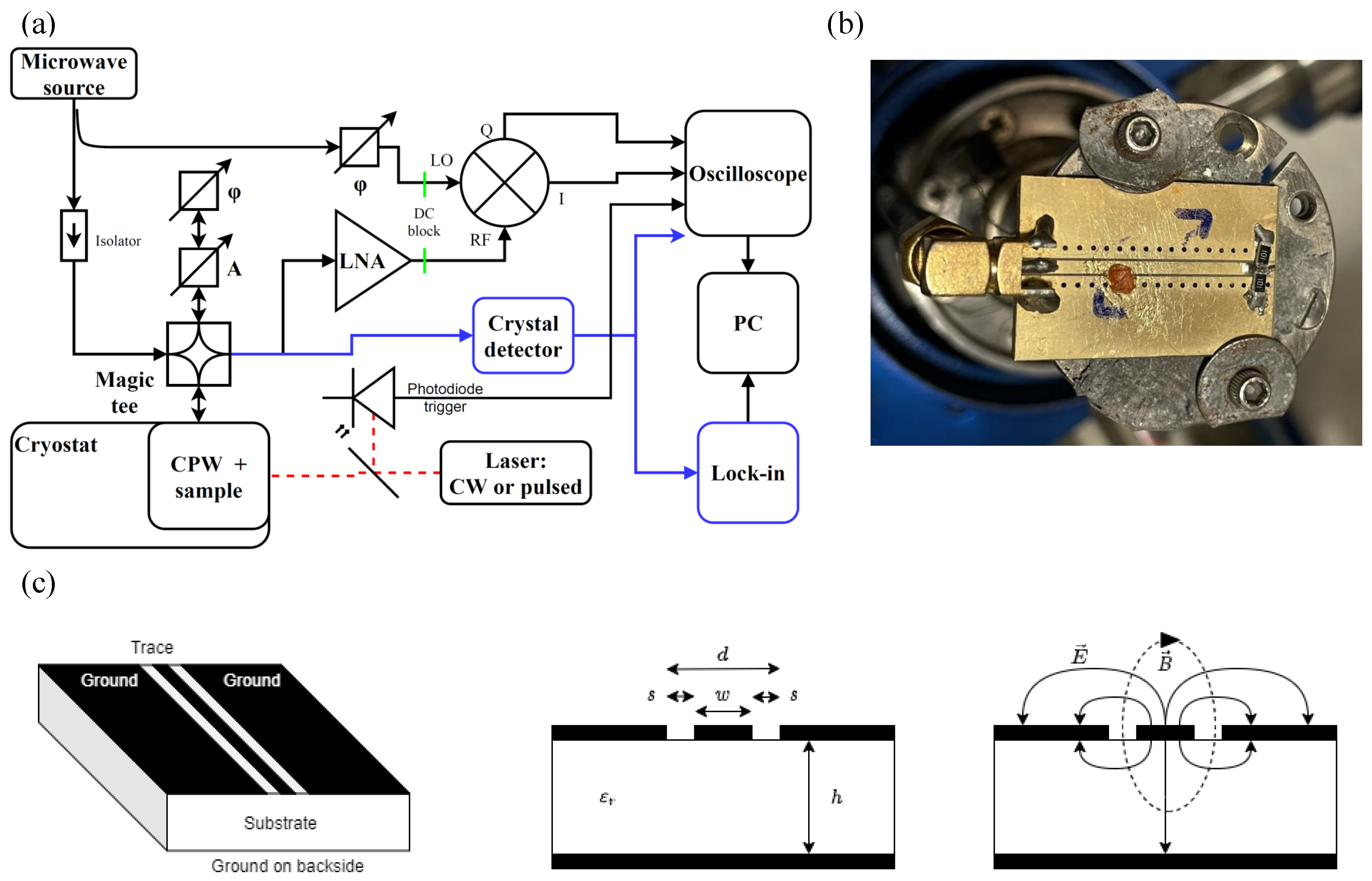
2.2. The Experimental Setup
2.3. Method of Detection
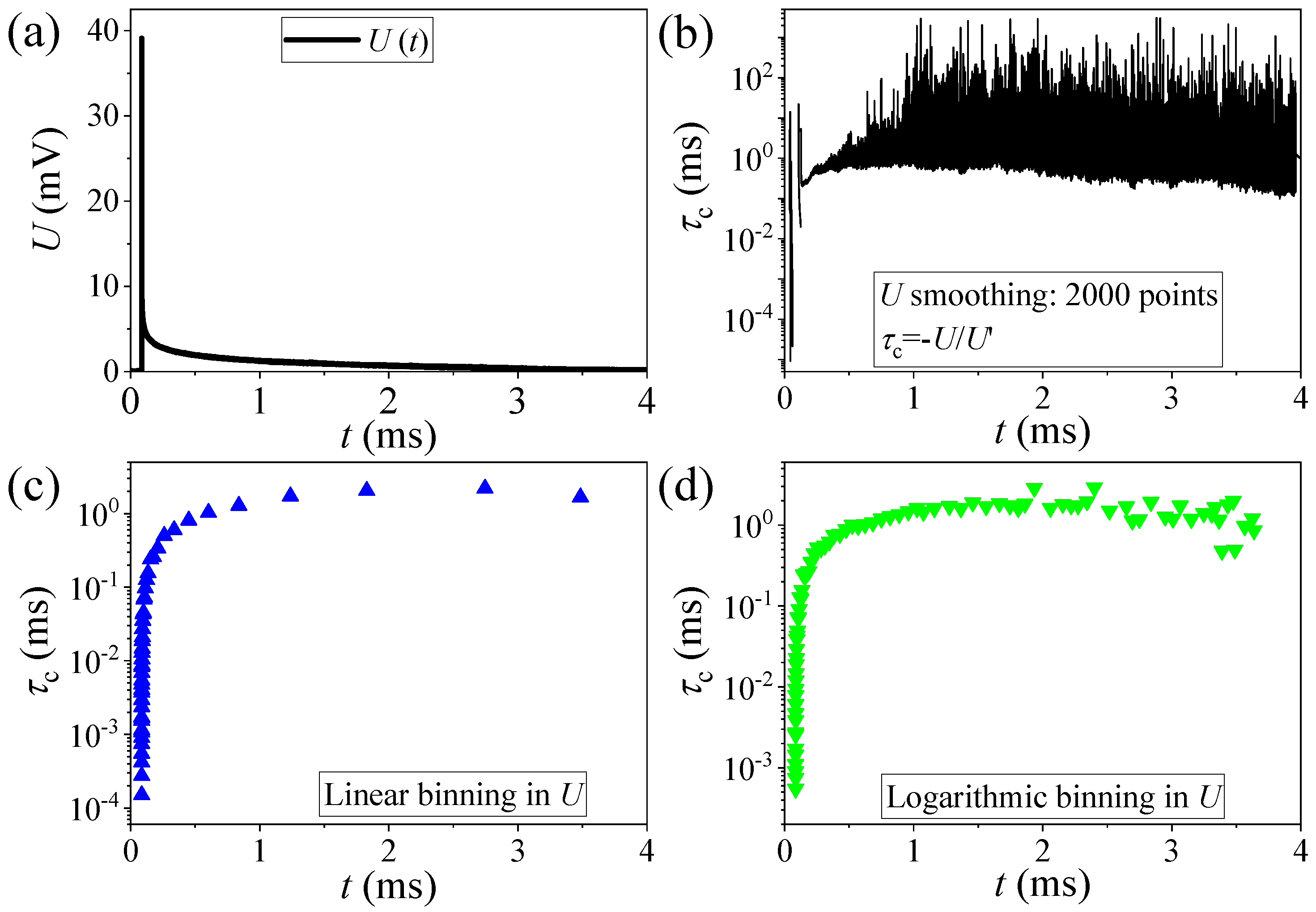
2.4. Analysis of the Data
3. Results
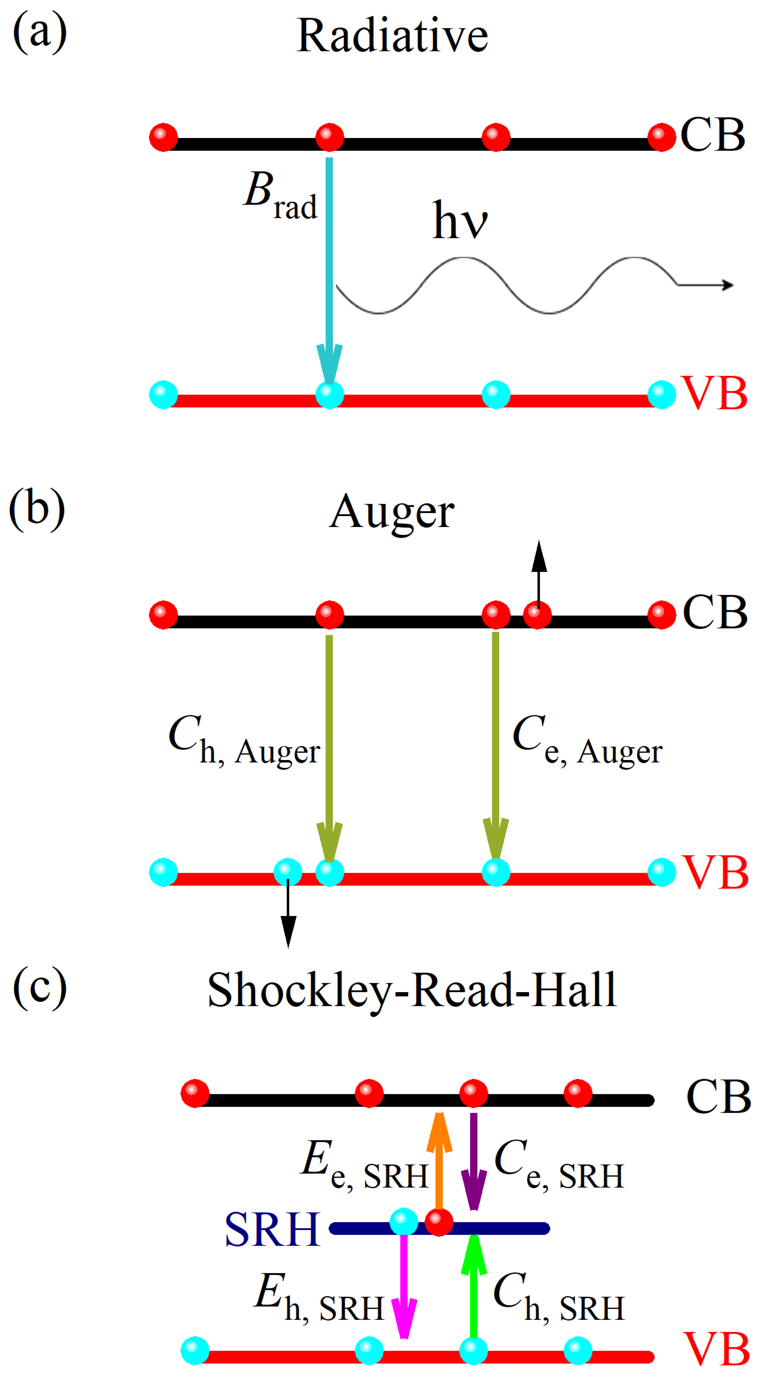
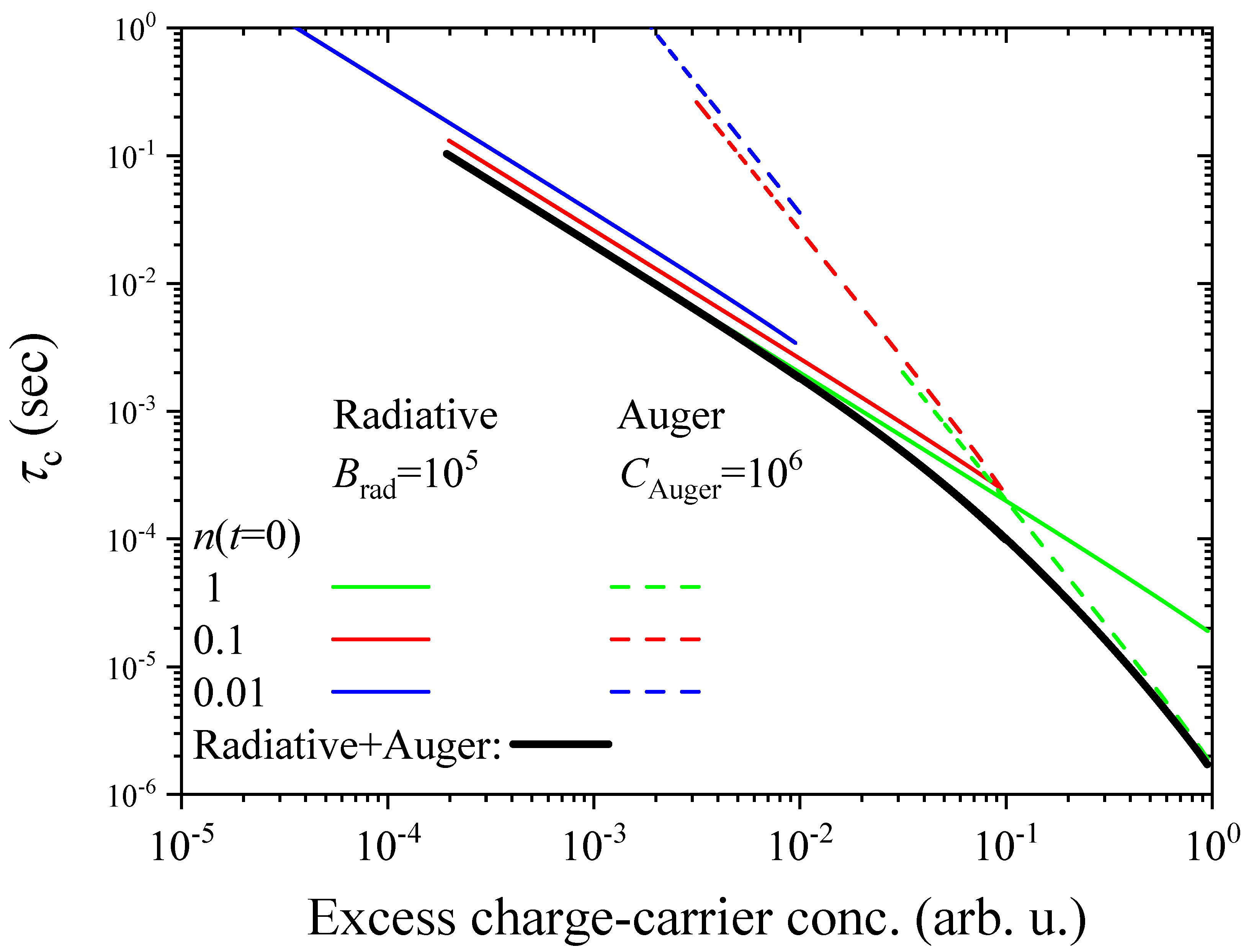
4. Discussion
5. Conclusions
Supplementary Materials
Author Contributions
Funding
Data Availability Statement
Conflicts of Interest
References
- Correa-Baena, J.P.; Saliba, M.; Buonassisi, T.; Graetzel, M.; Abate, A.; Tress, W.; Hagfeldt, A. Promises and challenges of perovskite solar cells. Science 2017, 358, 739–744. [Google Scholar] [CrossRef] [PubMed]
- Huang, J.; Yuan, Y.; Shao, Y.; Yan, Y. Understanding the physical properties of hybrid perovskites for photovoltaic applications. Nat. Rev. Mater. 2017, 2, 17042. [Google Scholar] [CrossRef]
- Lin, K.; Xing, J.; Quan, L.N.; de Arquer, F.P.G.; Gong, X.; Lu, J.; Xie, L.; Zhao, W.; Zhang, D.; Yan, C.; et al. Perovskite light-emitting diodes with external quantum efficiency exceeding 20 per cent. Nature 2018, 562, 245–248. [Google Scholar] [CrossRef] [PubMed]
- Protesescu, L.; Yakunin, S.; Bodnarchuk, M.I.; Krieg, F.; Caputo, R.; Hendon, C.H.; Yang, R.X.; Walsh, A.; Kovalenko, M.V. Nanocrystals of Cesium Lead Halide Perovskites (CsPbX3, X = Cl, Br, and I): Novel Optoelectronic Materials Showing Bright Emission with Wide Color Gamut. Nano Lett. 2015, 15, 3692–3696. [Google Scholar] [CrossRef]
- Zhang, F.; Zhong, H.; Chen, C.; Wu, X.g.; Hu, X.; Huang, H.; Han, J.; Zou, B.; Dong, Y. Brightly Luminescent and Color-Tunable Colloidal CH3NH3PbX3 (X = Br, I, Cl) Quantum Dots: Potential Alternatives for Display Technology. ACS Nano 2015, 9, 4533–4542. [Google Scholar] [CrossRef]
- Singha, A.; Paul, A.; Koul, S.; Sharma, V.; Mallick, S.; Balasubramaniam, K.R.; Kabra, D. Stable and Efficient Large-Area 4T Si/perovskite Tandem Photovoltaics with Sputtered Transparent Contact. Sol. RRL 2023, 7, 2300117. [Google Scholar] [CrossRef]
- Shamsi, J.; Rastogi, P.; Caligiuri, V.; Abdelhady, A.L.; Spirito, D.; Manna, L.; Krahne, R. Bright-Emitting Perovskite Films by Large-Scale Synthesis and Photoinduced Solid-State Transformation of CsPbBr3 Nanoplatelets. ACS Nano 2017, 11, 10206–10213. [Google Scholar] [CrossRef]
- Náfrádi, B.; Náfrádi, G.; Forró, L.; Horváth, E. Methylammonium Lead Iodide for Efficient X-ray Energy Conversion. J. Phys. Chem. C 2015, 119, 25204–25208. [Google Scholar] [CrossRef]
- Yakunin, S.; Dirin, D.N.; Shynkarenko, Y.; Morad, V.; Cherniukh, I.; Nazarenko, O.; Kreil, D.; Nauser, T.; Kovalenko, M.V. Detection of gamma photons using solution-grown single crystals of hybrid lead halide perovskites. Nat. Photon. 2016, 10, 585–589. [Google Scholar] [CrossRef]
- Andričević, P.; Náfrádi, G.; Kollár, M.; Náfrádi, B.; Lilley, S.; Kinane, C.; Frajtag, P.; Sienkiewicz, A.; Pautz, A.; Horváth, E.; et al. Hybrid halide perovskite neutron detectors. Sci. Rep. 2021, 11, 17159. [Google Scholar] [CrossRef]
- Mantulnikovs, K.; Glushkova, A.; Matus, P.; Ćirić, L.; Kollár, M.; Forró, L.; Horváth, E.; Sienkiewicz, A. Morphology and Photoluminescence of CH3NH3PbI3 Deposits on Nonplanar, Strongly Curved Substrates. ACS Photonics 2018, 5, 1476–1485. [Google Scholar] [CrossRef]
- Ho-Baillie, A.W.Y.; Sullivan, H.G.J.; Bannerman, T.A.; Talathi, H.P.; Bing, J.; Tang, S.; Xu, A.; Bhattacharyya, D.; Cairns, I.H.; McKenzie, D.R. Deployment Opportunities for Space Photovoltaics and the Prospects for Perovskite Solar Cells. Adv. Mater. Technol. 2022, 7, 2101059. [Google Scholar] [CrossRef]
- Pérez-del Rey, D.; Dreessen, C.; Igual-Muñoz, A.M.; van den Hengel, L.; Gélvez-Rueda, M.C.; Savenije, T.J.; Grozema, F.C.; Zimmermann, C.; Bolink, H.J. Perovskite Solar Cells: Stable under Space Conditions. Sol. RRL 2020, 4, 2000447. [Google Scholar] [CrossRef]
- Dey, A.; Ye, J.; De, A.; Debroye, E.; Ha, S.K.; Bladt, E.; Kshirsagar, A.S.; Wang, Z.; Yin, J.; Wang, Y.; et al. State of the Art and Prospects for Halide Perovskite Nanocrystals. ACS Nano 2021, 15, 10775–10981. [Google Scholar] [CrossRef]
- Manser, J.S.; Christians, J.A.; Kamat, P.V. Intriguing Optoelectronic Properties of Metal Halide Perovskites. Chem. Rev. 2016, 116, 12956–13008. [Google Scholar] [CrossRef]
- Kamat, P.V.; Bisquert, J.; Buriak, J. Lead-Free Perovskite Solar Cells. ACS Energy Lett. 2017, 2, 904–905. [Google Scholar] [CrossRef]
- Schanze, K.S.; Kamat, P.V.; Yang, P.; Bisquert, J. Progress in Perovskite Photocatalysis. ACS Energy Lett. 2020, 5, 2602–2604. [Google Scholar] [CrossRef]
- Vasiljevic, M.; Kollár, M.; Spirito, D.; Riemer, L.; Forró, L.; Horváth, E.; Gorfman, S.; Damjanovic, D. “Forbidden” Polarisation and Extraordinary Piezoelectric Effect in Organometallic Lead Halide Perovskites. Adv. Funct. Mater. 2022, 32, 2204898. [Google Scholar] [CrossRef]
- Yuan, Y.; Chae, J.; Shao, Y.; Wang, Q.; Xiao, Z.; Centrone, A.; Huang, J. Photovoltaic Switching Mechanism in Lateral Structure Hybrid Perovskite Solar Cells. Adv. Energy Mater. 2015, 5. [Google Scholar] [CrossRef]
- Bernard, G.M.; Wasylishen, R.E.; Ratcliffe, C.I.; Terskikh, V.; Wu, Q.; Buriak, J.M.; Hauger, T. Methylammonium Cation Dynamics in Methylammonium Lead Halide Perovskites: A Solid-State NMR Perspective. J. Phys. Chem. A 2018, 122, 1560–1573. [Google Scholar] [CrossRef]
- Tian, J.; Xue, Q.; Yao, Q.; Li, N.; Brabec, C.J.; Yip, H.L. Inorganic Halide Perovskite Solar Cells: Progress and Challenges. Adv. Energy Mater. 2020, 10, 2000183. [Google Scholar] [CrossRef]
- Møller, C.K. Crystal Structure and Photoconductivity of Cæsium Plumbohalides. Nature 1958, 182, 1436. [Google Scholar] [CrossRef]
- Hu, Y.; Aygüler, M.F.; Petrus, M.L.; Bein, T.; Docampo, P. Impact of Rubidium and Cesium Cations on the Moisture Stability of Multiple-Cation Mixed-Halide Perovskites. ACS Energy Lett. 2017, 2, 2212–2218. [Google Scholar] [CrossRef]
- Clinckemalie, L.; Valli, D.; Roeffaers, M.B.J.; Hofkens, J.; Pradhan, B.; Debroye, E. Challenges and Opportunities for CsPbBr3 Perovskites in Low- and High-Energy Radiation Detection. ACS Energy Lett. 2021, 6, 1290–1314. [Google Scholar] [CrossRef]
- Zhou, Y.; Zhao, Y. Chemical stability and instability of inorganic halide perovskites. Energy Environ. Sci. 2019, 12, 1495–1511. [Google Scholar] [CrossRef]
- Haruta, Y.; Ikenoue, T.; Miyake, M.; Hirato, T. One-Step Coating of Full-Coverage CsPbBr3 Thin Films via Mist Deposition for All-Inorganic Perovskite Solar Cells. ACS Appl. Energy Mater. 2020, 3, 11523–11528. [Google Scholar] [CrossRef]
- Fu, Y.; Zhu, H.; Stoumpos, C.C.; Ding, Q.; Wang, J.; Kanatzidis, M.G.; Zhu, X.; Jin, S. Broad Wavelength Tunable Robust Lasing from Single-Crystal Nanowires of Cesium Lead Halide Perovskites (CsPbX3, X = Cl, Br, I). ACS Nano 2016, 10, 7963–7972. [Google Scholar] [CrossRef]
- Eaton, S.W.; Lai, M.; Gibson, N.A.; Wong, A.B.; Dou, L.; Ma, J.; Wang, L.W.; Leone, S.R.; Yang, P. Lasing in robust cesium lead halide perovskite nanowires. Proc. Natl. Acad. Sci. USA 2016, 113, 1993–1998. [Google Scholar] [CrossRef]
- Ding, J.; Du, S.; Zuo, Z.; Zhao, Y.; Cui, H.; Zhan, X. High Detectivity and Rapid Response in Perovskite CsPbBr3 Single-Crystal Photodetector. J. Phys. Chem. C 2017, 121, 4917–4923. [Google Scholar] [CrossRef]
- Stoumpos, C.C.; Malliakas, C.D.; Peters, J.A.; Liu, Z.; Sebastian, M.; Im, J.; Chasapis, T.C.; Wibowo, A.C.; Chung, D.Y.; Freeman, A.J.; et al. Crystal Growth of the Perovskite Semiconductor CsPbBr3: A New Material for High-Energy Radiation Detection. Cryst. Growth Des. 2013, 13, 2722–2727. [Google Scholar] [CrossRef]
- Liao, M.; Shan, B.; Li, M. Role of Trap States in Excitation Wavelength-Dependent Photoluminescence of Strongly Quantum-Confined All-Inorganic CsPbBr3 Perovskites with Varying Dimensionalities. J. Phys. Chem. C 2021, 125, 21062–21069. [Google Scholar] [CrossRef]
- Zhang, Y.; Guo, T.; Yang, H.; Bose, R.; Liu, L.; Yin, J.; Han, Y.; Bakr, O.M.; Mohammed, O.F.; Malko, A.V. Emergence of multiple fluorophores in individual cesium lead bromide nanocrystals. Nat. Commun. 2019, 10, 2930. [Google Scholar] [CrossRef] [PubMed]
- Akkerman, Q.A.; Motti, S.G.; Srimath Kandada, A.R.; Mosconi, E.; D’Innocenzo, V.; Bertoni, G.; Marras, S.; Kamino, B.A.; Miranda, L.; De Angelis, F.; et al. Solution Synthesis Approach to Colloidal Cesium Lead Halide Perovskite Nanoplatelets with Monolayer-Level Thickness Control. J. Am. Chem. Soc. 2016, 138, 1010–1016. [Google Scholar] [CrossRef] [PubMed]
- Liang, Z.; Zhao, S.; Xu, Z.; Qiao, B.; Song, P.; Gao, D.; Xu, X. Shape-Controlled Synthesis of All-Inorganic CsPbBr3 Perovskite Nanocrystals with Bright Blue Emission. ACS Appl. Mater. Interfaces 2016, 8, 28824–28830. [Google Scholar] [CrossRef] [PubMed]
- Zhang, X.; Pang, G.; Xing, G.; Chen, R. Temperature dependent optical characteristics of all-inorganic CsPbBr3 nanocrystals film. Mater. Today Phys. 2020, 15, 100259. [Google Scholar] [CrossRef]
- Lobo, N.; Kawane, T.; Matt, G.J.; Osvet, A.; Shrestha, S.; Ievgen, L.; Brabec, C.J.; Kanak, A.; Fochuk, P.; Kato, M. Trapping effects and surface/interface recombination of carrier recombination in single- or poly-crystalline metal halide perovskites. Jpn. J. Appl. Phys. 2022, 61, 125503. [Google Scholar] [CrossRef]
- Gélvez-Rueda, M.C.; Fridriksson, M.B.; Dubey, R.K.; Jager, W.F.; van der Stam, W.; Grozema, F.C. Overcoming the exciton binding energy in two-dimensional perovskite nanoplatelets by attachment of conjugated organic chromophores. Nat. Commun. 2020, 11, 1901. [Google Scholar] [CrossRef]
- Kunst, M.; Beck, G. The study of charge carrier kinetics in semiconductors by microwave conductivity measurements. J. Appl. Phys. 1986, 60, 3558–3566. [Google Scholar] [CrossRef]
- Kunst, M.; Beck, G. The study of charge carrier kinetics in semiconductors by microwave conductivity measurements. II. J. Appl. Phys. 1988, 63, 1093–1098. [Google Scholar] [CrossRef]
- Li, Y.; Jia, Z.; Yang, Y.; Yao, F.; Liu, Y.; Lin, Q. Shallow traps-induced ultra-long lifetime of metal halide perovskites probed with light-biased time-resolved microwave conductivity. Appl. Phys. Rev. 2023, 10, 011406. [Google Scholar] [CrossRef]
- Savenije, T.J.; Guo, D.; Caselli, V.M.; Hutter, E.M. Quantifying Charge-Carrier Mobilities and Recombination Rates in Metal Halide Perovskites from Time-Resolved Microwave Photoconductivity Measurements. Adv. Energy Mater. 2020, 10, 1903788. [Google Scholar] [CrossRef]
- Yao, F.; Lin, Q. Charge Carrier Dynamics of Organic Cation-Treated Perovskites Probed with Time-Resolved Microwave Conductivity. ACS Photonics 2022, 9, 3165–3171. [Google Scholar] [CrossRef]
- Bojtor, A.; Krisztián, D.; Korsós, F.; Kollarics, S.; Paráda, G.; Pinel, T.; Kollár, M.; Horváth, E.; Mettan, X.; Shiozawa, H.; et al. Millisecond-Scale Charge-Carrier Recombination Dynamics in the CsPbBr3 Perovskite. Adv. Energy Sustain. Res. 2024, 5, 2400043. [Google Scholar] [CrossRef]
- Dirin, D.N.; Cherniukh, I.; Yakunin, S.; Shynkarenko, Y.; Kovalenko, M.V. Solution-Grown CsPbBr3 Perovskite Single Crystals for Photon Detection. Chem. Mater. 2016, 28, 8470–8474. [Google Scholar] [CrossRef] [PubMed]
- Saidaminov, M.I.; Abdelhady, A.L.; Maculan, G.; Bakr, O.M. Retrograde solubility of formamidinium and methylammonium lead halide perovskites enabling rapid single crystal growth. Chem. Commun. 2015, 51, 17658–17661. [Google Scholar] [CrossRef] [PubMed]
- Saidaminov, M.I.; Abdelhady, A.L.; Murali, B.; Alarousu, E.; Burlakov, V.M.; Peng, W.; Dursun, I.; Wang, L.; He, Y.; Maculan, G.; et al. High-quality bulk hybrid perovskite single crystals within minutes by inverse temperature crystallization. Nat. Commun. 2015, 6, 7586. [Google Scholar] [CrossRef]
- Simons, R.N. Coplanar Waveguide Circuits Components & Systems, 1st ed.; Wiley-IEEE Press: Hoboken, NJ, USA, 2001. [Google Scholar]
- Pozar, D. Microwave Engineering—Solutions Manual, 4th ed.; Wiley: Hoboken, NJ, USA, 2011. [Google Scholar]
- Lauer, K.; Laades, A.; übensee, H.; Metzner, H.; Lawerenz, A. Detailed analysis of the microwave-detected photoconductance decay in crystalline silicon. J. Appl. Phys. 2008, 104, 104503. [Google Scholar] [CrossRef]
- Saidaminov, M.I.; Haque, M.A.; Almutlaq, J.; Sarmah, S.; Miao, X.H.; Begum, R.; Zhumekenov, A.A.; Dursun, I.; Cho, N.; Murali, B.; et al. Inorganic Lead Halide Perovskite Single Crystals: Phase-Selective Low-Temperature Growth, Carrier Transport Properties, and Self-Powered Photodetection. Adv. Opt. Mater. 2017, 5, 1600704. [Google Scholar] [CrossRef]
- Bisquert, J.; Fabregat-Santiago, F.; Mora-Seró, I.; Garcia-Belmonte, G.; Giménez, S. Electron Lifetime in Dye-Sensitized Solar Cells: Theory and Interpretation of Measurements. J. Phys. Chem. C 2009, 113, 17278–17290. [Google Scholar] [CrossRef]
- Milot, R.L.; Eperon, G.E.; Snaith, H.J.; Johnston, M.B.; Herz, L.M. Temperature-Dependent Charge-Carrier Dynamics in CH3NH3PbI3 Perovskite Thin Films. Adv. Funct. Mater. 2015, 25, 6218–6227. [Google Scholar] [CrossRef]
- Sinton, R.A.; Cuevas, A.; Stuckings, M. Quasi-steady-state photoconductance, a new method for solar cell material and device characterization. In Proceedings of the Conference Record of the Twenty Fifth IEEE Photovoltaic Specialists Conference-1996, Washington, DC, USA, 13–17 May 1996; pp. 457–460. [Google Scholar]
- Goodarzi, M.; Sinton, R.; Macdonald, D. Quasi-steady-state photoconductance bulk lifetime measurements on silicon ingots with deeper photogeneration. AIP Adv. 2019, 9, 015128. [Google Scholar] [CrossRef]
- Wilson, M.; Savtchouk, A.; Lagowski, J.; Kis-Szabo, K.; Korsos, F.; Toth, A.; Kopecek, R.; Mihailetchi, V. QSS-μPCD measurement of lifetime in silicon wafers: Advantages and new applications. Energy Procedia 2011, 8, 128–134. [Google Scholar] [CrossRef]
- Gyüre-Garami, B.; Blum, B.; Sági, O.; Bojtor, A.; Kollarics, S.; Csősz, G.; Márkus, B.G.; Volk, J.; Simon, F. Ultrafast sensing of photoconductivity decay using microwave resonators. J. Appl. Phys. 2019, 126, 235702. [Google Scholar] [CrossRef]
- Trimpl, M.J.; Wright, A.D.; Schutt, K.; Buizza, L.R.V.; Wang, Z.; Johnston, M.B.; Snaith, H.J.; Mueller-Buschbaum, P.; Herz, L.M. Charge-Carrier Trapping and Radiative Recombination in Metal Halide Perovskite Semiconductors. Adv. Funct. Mater. 2020, 30, 2004312. [Google Scholar] [CrossRef]
- Zhang, M.; Zheng, Z.; Fu, Q.; Guo, P.; Zhang, S.; Chen, C.; Chen, H.; Wang, M.; Luo, W.; Tian, Y. Determination of Defect Levels in Melt-Grown All-Inorganic Perovskite CsPbBr3 Crystals by Thermally Stimulated Current Spectra. J. Phys. Chem. C 2018, 122, 10309–10315. [Google Scholar] [CrossRef]
- Kang, J.; Wang, L.W. High Defect Tolerance in Lead Halide Perovskite CsPbBr3. J. Phys. Chem. Lett. 2017, 8, 489–493. [Google Scholar] [CrossRef]
- Rein, S. Lifetime Spectroscopy, 1st ed.; Springer: Berlin/Heidelberg, Germany, 2005. [Google Scholar]
- Shockley, W.; Read, W.T. Statistics of the Recombinations of Holes and Electrons. Phys. Rev. 1952, 87, 835–842. [Google Scholar] [CrossRef]
- Hall, R.N. Electron-Hole Recombination in Germanium. Phys. Rev. 1952, 87, 387. [Google Scholar] [CrossRef]
- Hall, R. Recombination processes in semiconductors. Proc. Inst. Electr. Eng. Part B 1959, 106, 923–931. [Google Scholar] [CrossRef]
- Schroder, D. Semiconductor Material and Device Characterization; IEEE Press, Wiley: Hoboken, NJ, USA, 2006. [Google Scholar]
- Liu, Y.; Yang, Z.; Cui, D.; Ren, X.; Sun, J.; Liu, X.; Zhang, J.; Wei, Q.; Fan, H.; Yu, F.; et al. Two-Inch-Sized Perovskite CH3NH3PbX3 (X = Cl, Br, I) Crystals: Growth and Characterization. Adv. Mater. 2015, 27, 5176–5183. [Google Scholar] [CrossRef]
- Knox, R.S. Theory of Excitons. In Solid State Physics; Seitz, F., Turnbull, D., Eds.; Academic Press: New York, NY, USA, 1963; Volume 5. [Google Scholar]
- Nguyen, X.T.; Winte, K.; Timmer, D.; Rakita, Y.; Ceratti, D.R.; Aharon, S.; Ramzan, M.S.; Cocchi, C.; Lorke, M.; Jahnke, F.; et al. Phonon-driven intra-exciton Rabi oscillations in CsPbBr3 halide perovskites. Nat. Commun. 2023, 14, 1047. [Google Scholar] [CrossRef] [PubMed]
- Sólyom, J. Fundamentals of the Physics of Solids II: Electronic Properties; Springer: Berlin/Heidelberg, Germany, 2008. [Google Scholar]
- Bleichner, H.; Jonsson, P.; Keskitalo, N.; Nordlander, E. Temperature and injection dependence of the Shockley–Read–Hall lifetime in electron irradiated n-type silicon. J. Appl. Phys. 1996, 79, 9142–9148. [Google Scholar] [CrossRef]
- Keskitalo, N.; Jonsson, P.; Nordgren, K.; Bleichner, H.; Nordlander, E. Temperature and injection dependence of the Shockley–Read–Hall lifetime in electron-irradiated p-type silicon. J. Appl. Phys. 1998, 83, 4206–4212. [Google Scholar] [CrossRef]

Disclaimer/Publisher’s Note: The statements, opinions and data contained in all publications are solely those of the individual author(s) and contributor(s) and not of MDPI and/or the editor(s). MDPI and/or the editor(s) disclaim responsibility for any injury to people or property resulting from any ideas, methods, instructions or products referred to in the content. |
© 2024 by the authors. Licensee MDPI, Basel, Switzerland. This article is an open access article distributed under the terms and conditions of the Creative Commons Attribution (CC BY) license (https://creativecommons.org/licenses/by/4.0/).
Share and Cite
Bojtor, A.; Krisztián, D.; Korsós, F.; Kollarics, S.; Paráda, G.; Kollár, M.; Horváth, E.; Mettan, X.; Márkus, B.G.; Forró, L.; et al. Dynamics of Photoinduced Charge Carriers in Metal-Halide Perovskites. Nanomaterials 2024, 14, 1742. https://doi.org/10.3390/nano14211742
Bojtor A, Krisztián D, Korsós F, Kollarics S, Paráda G, Kollár M, Horváth E, Mettan X, Márkus BG, Forró L, et al. Dynamics of Photoinduced Charge Carriers in Metal-Halide Perovskites. Nanomaterials. 2024; 14(21):1742. https://doi.org/10.3390/nano14211742
Chicago/Turabian StyleBojtor, András, Dávid Krisztián, Ferenc Korsós, Sándor Kollarics, Gábor Paráda, Márton Kollár, Endre Horváth, Xavier Mettan, Bence G. Márkus, László Forró, and et al. 2024. "Dynamics of Photoinduced Charge Carriers in Metal-Halide Perovskites" Nanomaterials 14, no. 21: 1742. https://doi.org/10.3390/nano14211742
APA StyleBojtor, A., Krisztián, D., Korsós, F., Kollarics, S., Paráda, G., Kollár, M., Horváth, E., Mettan, X., Márkus, B. G., Forró, L., & Simon, F. (2024). Dynamics of Photoinduced Charge Carriers in Metal-Halide Perovskites. Nanomaterials, 14(21), 1742. https://doi.org/10.3390/nano14211742