Article

Design and Simulation for Minimizing Non-Radiative Recombination Losses in CsGeI2Br Perovskite Solar Cells

1
Institute of Advanced Materials, Jiangsu Provincial Engineering Research Center of Low Dimensional Physics and New Energy, School of Science, Nanjing University of Posts and Telecommunications (NJUPT), Nanjing 210023, China
2
School of Physics and Electronic Information, Jiangsu Second Normal University, Nanjing 210023, China
*
Authors to whom correspondence should be addressed.
Nanomaterials 2024, 14(20), 1650; https://doi.org/10.3390/nano14201650
Submission received: 19 September 2024 / Revised: 11 October 2024 / Accepted: 12 October 2024 / Published: 14 October 2024
(This article belongs to the Special Issue Perovskite Nanostructures: Synthesis, Properties and Applications)

Abstract

:
CsGeI2Br-based perovskites, with their favorable band gap and high absorption coefficient, are promising candidates for the development of efficient lead-free perovskite solar cells (PSCs). However, bulk and interfacial carrier non-radiative recombination losses hinder the further improvement of power conversion efficiency and stability in PSCs. To overcome this challenge, the photovoltaic potential of the device is unlocked by optimizing the optical and electronic parameters through rigorous numerical simulation, which include tuning perovskite thickness, bulk defect density, and series and shunt resistance. Additionally, to make the simulation data as realistic as possible, recombination processes, such as Auger recombination, must be considered. In this simulation, when the Auger capture coefficient is increased to 10−29 cm6 s−1, the efficiency drops from 31.62% (without taking Auger recombination into account) to 29.10%. Since Auger recombination is unavoidable in experiments, carrier losses due to Auger recombination should be included in the analysis of the efficiency limit to avoid significantly overestimating the simulated device performance. Therefore, this paper provides valuable insights for designing realistic and efficient lead-free PSCs.

1. Introduction

Hybrid organic–inorganic perovskite solar cells, as an efficient and low-cost photovoltaic technology for capturing solar energy, have emerged as one of the most active research fields in photovoltaic technology [1,2,3,4]. The power conversion efficiency (PCE) of single-junction PSCs has improved significantly over the past decade, increasing from the initial 3.8% to the latest certified value of 26.1% [5]. This advancement fully demonstrates the vast potential and rapid development of PSC technology. Currently, the highest PCE achieved by this technology has matched the efficiency of some commercial solar cells on the market, such as copper indium gallium selenide (CIGS) solar cells and crystalline silicon. In the four-terminal configuration of all-perovskite stacked PSCs, the PCE has reached an impressive level above 27% [6], and perovskite-silicon stacked solar cells have even surpassed the 34% efficiency threshold [7]. The notable advancements are attributed to the superior characteristics of metal halide perovskite, as well as the rapid assimilation of lessons from other photovoltaic technologies, such as dye-sensitized solar cells, organic photovoltaics, and silicon solar cells. However, despite the remarkable breakthrough in performance, the stability issue of PSC technology and lead toxicity still limits its commercialization. To overcome this challenge, researchers have begun to explore new material systems, among which lead-free cesium compounds have attracted much attention for their excellent photovoltaic performance and tunable energy-band structure. Cesium lead-free halide PSCs not only have higher photovoltaic conversion efficiency but also have significant advantages in terms of cost and material safety, which are expected to promote the sustainable development of the photovoltaic industry [8,9].
CsGeI2Br has attracted considerable interest within the perovskite industry due to its non-toxic composition, together with its 1.579 eV band gap, high absorption coefficient (over 105 cm−1) in the visible range, and conductivity [10,11]. Recent studies have shown that compared to organic–inorganic hybrid perovskites, cesium lead-free halide perovskites exhibit higher thermal stability. Among all lead-free inorganic PSCs, CsSnI3 achieves the highest PCE, reaching 11.21% [12]. Without considering non-radiative recombination, the simulation by Joy Sarkar and others using the solar cell capacitance simulator-one dimension (SCAPS-1D) version 3.3.10 employed Spiro-OMeTAD as the hole transport layer (HTL), TiO2 as the electron transport layer (ETL), and CsGeI2Br as the perovskite layer, achieving a device efficiency of 25.15%, open-circuit voltage (Voc) of 1.23 V, short-circuit current density (Jsc) of 26.42 mA/cm2, and fill factor (FF) of 77.74% [11]. Nonetheless, it is inescapable that non-radiative recombination losses are present across all categories of solar cells, mainly due to phenomena such as tail recombination, electron–phonon coupling, Auger recombination, and recombination facilitated by defects [13]. The performance characteristics of the record device, including the Voc, Jsc, FF, and PCE, are caused to deviate from the radiation limit by these losses [14,15,16,17]. Additionally, non-radiative recombination centers usually accelerate the degradation of perovskite absorbers, which hinders their development [18,19]. In order to further improve the performance of the device within the Shockley–Queisser (SQ) radiation limit and to improve the long-term stability of solar cells, it is extremely important to reduce all types of non-radiative recombination losses.
To unlock the full potential of CsGeI2Br-based PSCs, we have investigated their working mechanisms and optimization outcomes utilizing numerical simulations. The performance of PSCs is comprehensively assessed through a detailed examination of the optical/electrical parameters, which include perovskite thickness, bulk defect density, series and shunt resistance, and Auger recombination. The simulation results suggest that (1) bulk defects are identified as important factors limiting the device performance and (2) high shunt resistance, low series resistance, and appropriate Auger recombination coefficients reduce non-radiation recombination losses and improve a device’s Voc and FF, making it approach the theoretical calculated SQ limit efficiency. Therefore, this study provides guidance for researchers to optimize PSCs and ultimately approach the photovoltaic impact of the SQ radiation limit.

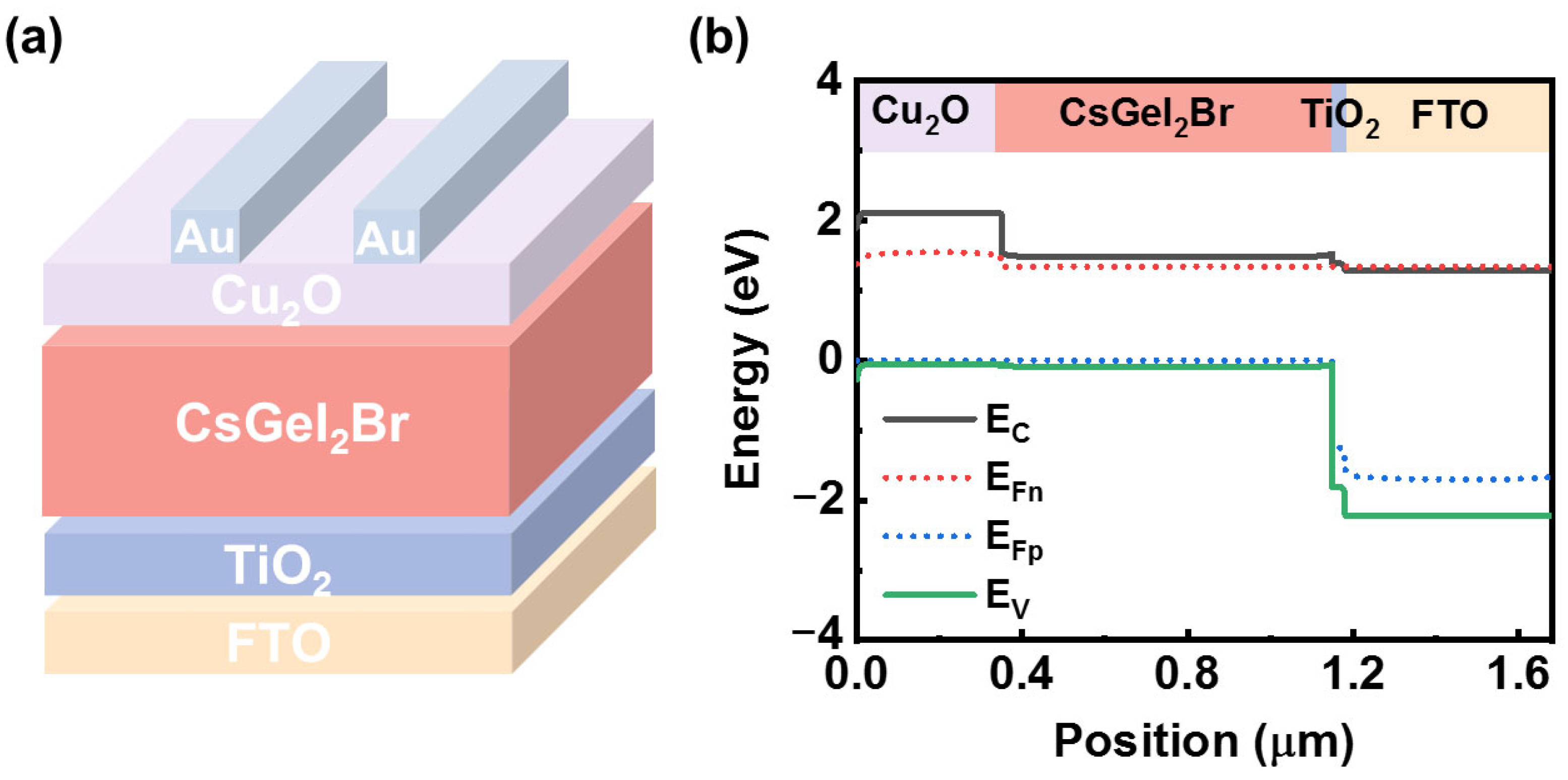
2. Theoretical Methods

SCAPS-1D is a widely used simulation software designed specifically for studying the electrical and optical properties of thin-film solar cells [20]. Detailed analyses of critical solar cell processes, such as carrier transport and recombination, are supported in one-dimensional structures. In this study, SCAPS-1D simulation software (Version 3.3.10) was employed. Given the increasing importance of numerical simulation for understanding, designing, and optimizing high-efficiency solar cells, the software was utilized to intuitively analyze cell parameters, enabling rapid and accurate predictions of cell performance. This, in turn, guided experiments and optimized the research and development process [21]. SCAPS-1D simulations are primarily based on Poisson’s equation, the continuity equations for electrons and holes (Equations (1)–(3)), constitutive equations (Equations (10) and (11)), and boundary conditions for semiconductor devices [22].
x ε 0 ε ψ ( x ) x = q p n + N D + N A + p t n t
J n x U n + G = n t
J p x U p + G = p t
where q is the amount of element charge; ε and ε0 stand for relative permittivity and free space permittivity, respectively; n and p are the electron and hole concentrations; Ψ is the potential; pt and nt are the hole and electron density distributions; ND+ and NA are the donor and acceptor concentrations; Jn and Jp are the electron and hole current density; G is the carrier generation rate; and Un and Up are the electron and hole recombination rate.
In general, the boundary conditions of hole and electron flow density and device potential are determined, the concentration of electron and hole and electric field can be solved, and other relevant working parameters of cell devices can be further obtained. Set the potential at the back contact to 0, then the boundary conditions at the back contact are as follows:
φ ( L ) = 0
J n ( L ) = q S n b [ n ( L ) n e q ( L ) ]
J p ( L ) = q S p b [ p ( L ) p e q ( L ) ]
The boundary conditions at the front contact are as follows:
φ ( 0 ) = φ f φ b + V a p p
J n ( 0 ) = q S n f [ n ( 0 ) n e q ( 0 ) ]
J p ( 0 ) = q S p f [ p ( 0 ) p e q ( 0 ) ]
The superscripts f and b denote the front and back electrodes, respectively, while Vapp represents the applied bias across the device. ψf and ψb indicate the work functions of the front and back contacts. neq(L), peq(L), neq(0), and peq(0) refer to the equilibrium concentrations of free electrons and holes at x = L and x = 0, respectively. p’ and n’ are the carrier concentrations at the contacts, and the surface recombination rates of holes and electrons at the front and back electrodes are denoted as Sp′f, Sn′f, Sp′b, and Sn′b, respectively.
The constitutive equations are as follows:
J n = μ n n q E F n x
J p = + μ p p q E F p x
The electron and hole quasi-Fermi levels are represented by EFn and EFp; μn and μp are electron and hole mobility. Together with appropriate boundary conditions at the interfaces and contacts, this results in a system of coupled differential equations in (Ψ, n, p) (Equations (1)–(3)) or (Ψ, EFn, EFp) (Equations (10) and (11)).
The simulation uses an AM1.5G light source of 1000 W/cm2 for constant lighting, and the temperature is set to 300 K. The device structure type used in the simulation is n-i-p, typically consisting of an FTO substrate, an ETL, a perovskite layer, an HTL, as well as a back-contact electrode system, and it is illustrated in Figure 1a, where Cu2O is chosen as the HTL and TiO2 as the ETL. Figure 1b shows the energy-level arrangement of the designed CsGeI2Br with the charge-transport layer. While series resistance (Rs) is 5 Ω cm2, shunt resistance (Rsh) is 5000 Ω cm2. The parameters for CsGeI2Br, Cu2O, and TiO2 are displayed in Table 1. Additionally, Table 2 presents the parameters for the interface defects between the CsGeI2Br layer and the transport layers, and these parameters are based on previous experiments and the published literature.

3. Results and Discussion

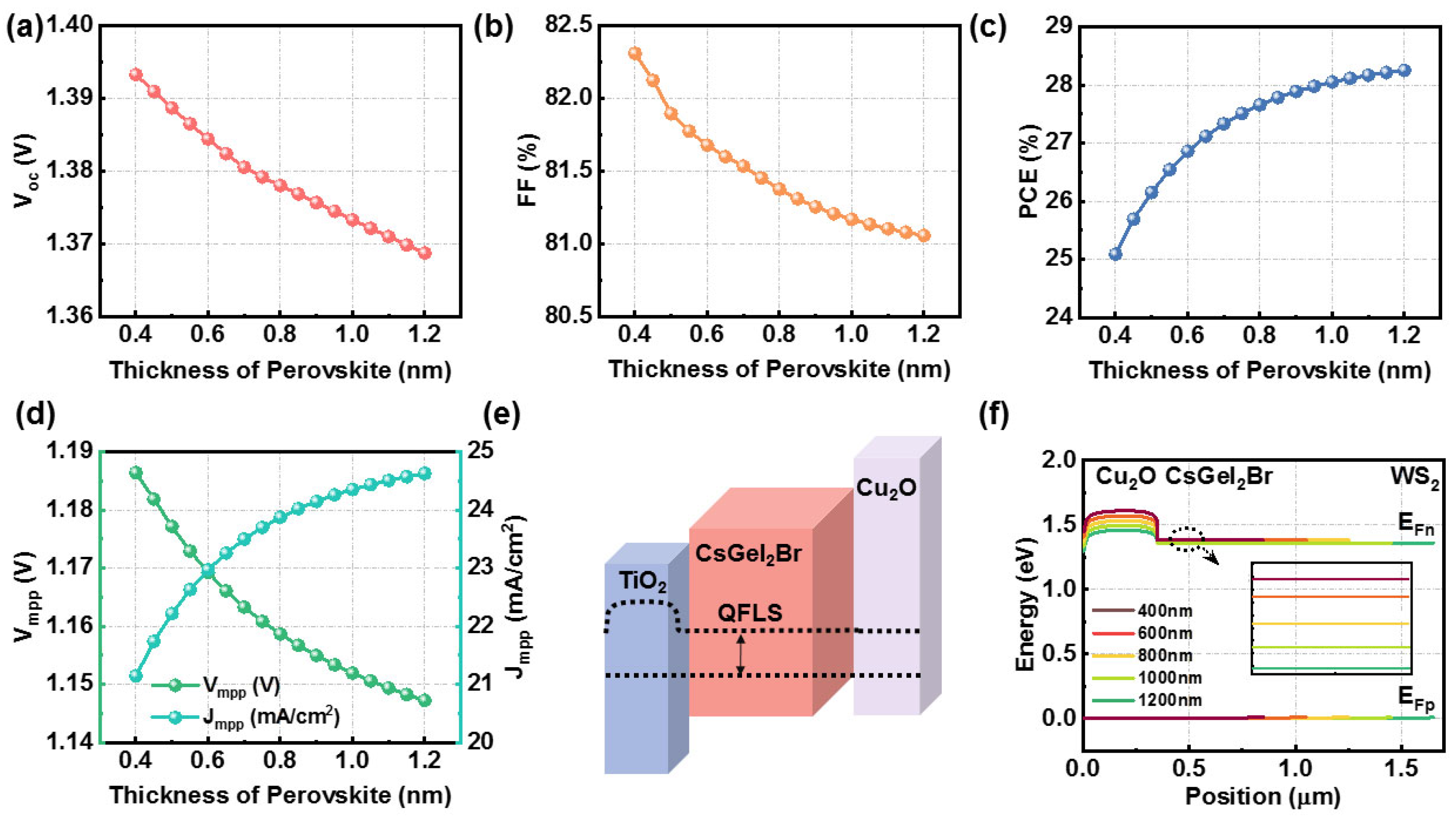
3.1. Dependence of Perovskite Thickness

The adjustment of perovskite material thickness significantly impacts its electrical, optical, and stability properties. Being too thin or too thick can reduce carrier transport efficiency, cause energy-level mismatches, degrade interface charge-transfer efficiency, and compromise stability. Precise thickness control is crucial for optimizing the performance of PSCs, aiming for the optimal PCE and stability [27,28]. This study examined thickness variations between 400 and 1200 nm, as depicted in Figure 2, which suggest the following: (i) Figure 2a reveals that as thickness increases, the Voc decreases from 1.37 V to 1.40 V due to an enhancement in the spectral response in the long-wavelength region [29]. (ii) With increasing thickness, both the Jsc and PCE show an upward trend, and the PCE increases from 25.09% to 28.25%. (iii) Conversely, the FF decreases as the thickness increases.
In detail, this is an important indicator of the conversion efficiency of a solar cell or electronic device. There is a specific mathematical relationship between the fill factor and parameters such as the Voc, Jsc, Vmmp, and Jmmp, and usually the FF is calculated as follows:
F F = V m p p × J m p p V o c × J s c
where Vmpp is maximum power voltage and Jmpp is maximum power current. Specifically, as the perovskite thickness increases, there is an increase in light scattering and absorption within the device, leading to a decrease in the Voc and Jsc. Additionally, with the increased thickness, the carrier transport distance within the device also increases, resulting in a reduction in Vmmp and an increase in Jmmp. These changes affect the calculated FF; thus, the overall trend is a decrease in the FF with increasing thickness.
To further comprehend the reason for the variation in the Voc, quasi-Fermi level splitting (QFLS) is a key factor impacting the Voc [30], with Equation (9) illustrating its relationship with the Voc. QFLS is defined as the difference between the electron quasi-Fermi level (EFe) and the hole quasi-Fermi level (EFh) (Figure 2e) [30].
V o c = Q F L S q = 1 q ( E F e E F h )
Figure 2f shows that as thickness increases, EFn remains constant while EFp decreases, leading to reduced QFLS and Voc. Thus, perovskite layer thickness significantly affects both QFLS and Voc. While greater thickness improves light absorption, it also increases non-radiative recombination and series resistance, further reducing QFLS and Voc. Studies suggest the optimal thickness is below 1000 nm. Based on experimental validation, 900 nm offers an ideal balance, enhancing absorption efficiency while minimizing recombination losses, ensuring both efficiency and stability [31,32].

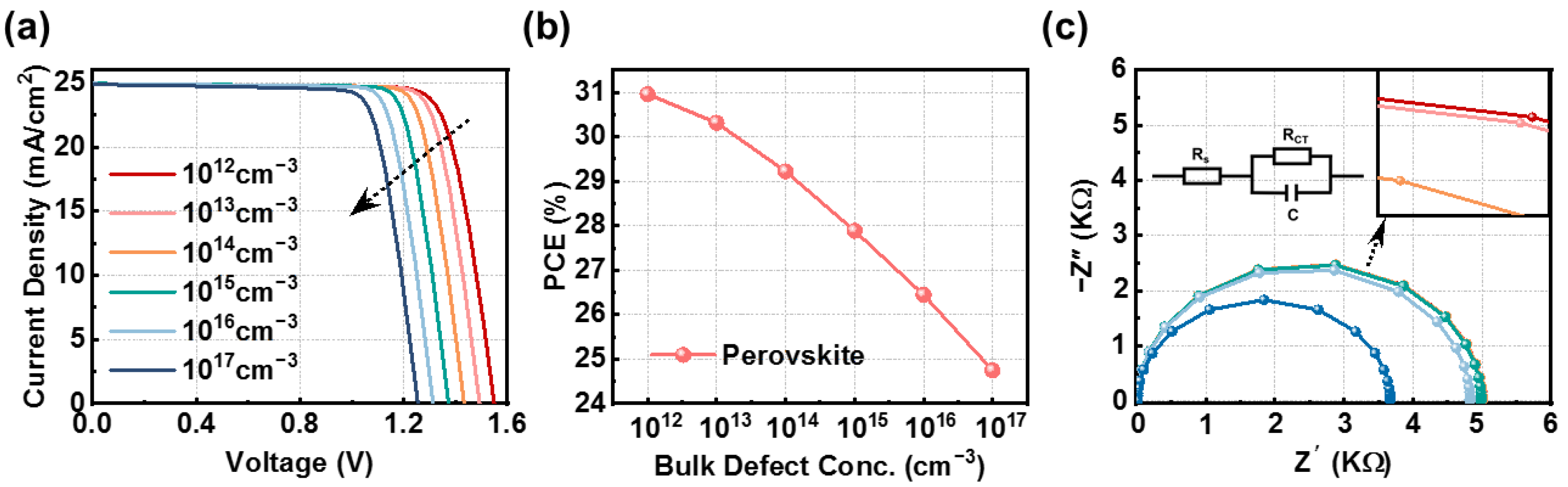
3.2. Dependence of Perovskite Bulk Defect Density

One of the primary impediments to the enhancement of PSC performance is the non-radiative recombination loss of bulk carriers. To enhance the device’s performance and stability, it is crucial to efficiently minimize the surface-related non-radiative recombination losses [33,34]. The bulk defect density (Nt) in CsGeI2Br-based PSCs is adjusted from 1012 cm−3 to 1017 cm−3 (Figure 3). As shown in Figure 3a, with the increase in Nt, both the Voc and Jsc decrease; however, the reduction in the Jsc is relatively small. This effect is due to the increase in the concentration of defects, which accelerates the recombination process of charge carriers inside the device, consequently decreasing the count of functional carriers and, consequently, a decrease in both the Voc and Jsc.
To further verify that lower Nt reduces interfacial charge recombination, electrochemical impedance spectroscopy (EIS) is used for measurements [35,36,37]. There are two processes that can contribute to EIS.
Z = Z j Z
The impedance is a complex number Z that can be expressed as two parts of the real part Z′ and the imaginary part Z″.
Z = R S + R C T 1 + ω 2 C 2 R C T 2
Here, Rs is the series resistance; RCT is the charge-transfer resistance, corresponding to the diameter of the semicircle in the Nyquist plot; and C is the capacitance. ω is the frequency.
Figure 3c shows the Nyquist curve for the CsGeI2Br device. In the context of EIS, key parameters such as the Rs, the RCT, and the recombination resistance (Rrec) can be derived from the measurement data. Rs is typically calculated from the initial intercept on the Z′ axis of the high-frequency arc in a Nyquist plot. At high frequencies, Rtr and the low-frequency Rrec correspond to the charge transfer at the HTL/perovskite interface and the recombination at the perovskite/ETL interface, respectively. Under light and high photoconductivity conditions, the Rrec predominantly contributes, given the negligible contribution of the RCT to the impedance response in high-performance PSCs [10,38]. The dominant semicircle in the Nyquist plot shown in Figure 3c is associated with the Rrec. As the Nt increases, the Rrec values corresponding to CsGeI2Br devices gradually decrease. The smaller the Rrec, the easier it is for carrier recombination within the perovskite, resulting in fewer electrons and holes being collected by the carrier layer, thereby reducing device performance [39]. Considering low doping is challenging, we chose Nt = 1014 cm−3 as the optimal value for enhanced device performance.

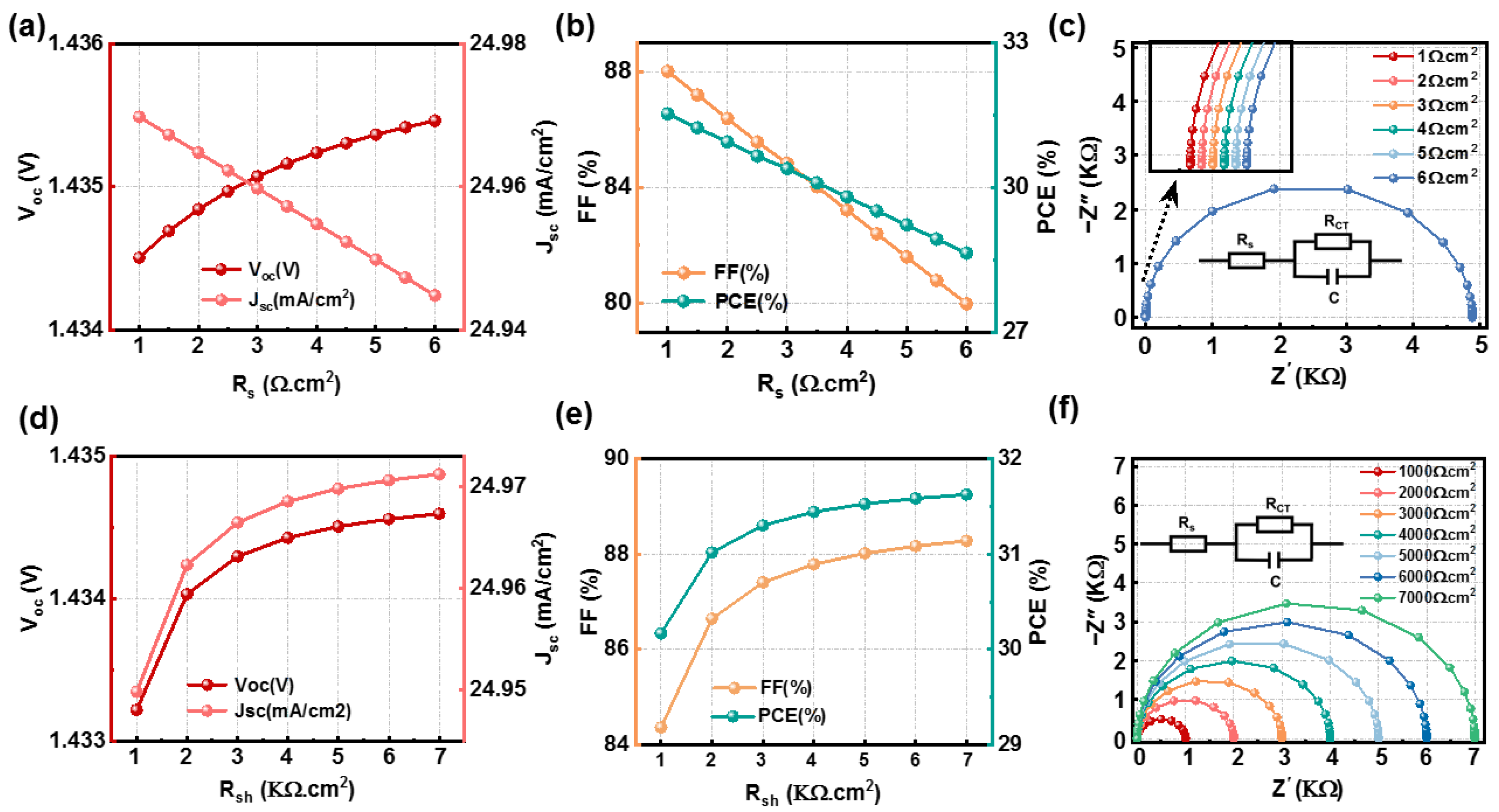
3.3. Dependence of Perovskite Series and Shunt Resistance

In PSCs, Rs and Rsh lead to energy loss, thereby diminishing overall efficiency. This encompasses the resistances contributed by the back contacts (Au), HTL, perovskite layer, ETL, and front contacts (FTO). These resistance effects are challenging to eliminate completely within solar cells. Therefore, it is important to conduct a thorough examination of these factors in order to enhance the efficiency of PSCs [40,41].
In this simulation study, Rs was varied from 1 to 6 Ω cm2 and Rsh from 1000 to 7000 Ω cm2, with the changes in photovoltaic parameters being examined, as depicted in Figure 4a,b from which we can conclude the following: (i) When the series resistance Rs increases, the Voc of the device only experiences a slight change, going from 1.4345 V to 1.4355 V, while there is a slight increase noted in the Jsc, moving from 24.95 mA/cm2 to 24.97 mA/cm2. Conversely, the reductions in the FF and PCE are notably more pronounced, decreasing from 80.00% to 88.01% and from 28.64% to 31.53%, respectively. As illustrated in Figure 4c, the increase in Rs results in a reduction in the semicircle radius in the Nyquist plot, indicating a weakening of the electric field strength. This leads to an increased likelihood of electron and hole recombination before reaching the electrodes due to interactions with defects, impurities, or interfaces within the device, thereby diminishing the overall efficiency of the PSC, so we chose Rs = 1 Ω cm2 as the optimal value for enhanced device performance. (ii) With the increase in Rsh (Rs = 1 Ω cm2), the Voc and Jsc are slightly affected, with the Voc dropping from 1.433V to 1.435V and the Jsc rising from 24.95 mA/cm2 to 24.97 mA/cm2. In contrast, Rsh increases cause more significant changes in the FF and PCE, with the FF decreasing from 84.37% to 88.28% and the PCE from 30.17% to 31.62%. Figure 4f illustrates that the Nyquist plot’s semicircle expands with rising Rsh, reflecting an increasing Rrec for the CsGeI2Br device. A higher Rrec reduces recombination in the perovskite, leading to more collected electrons and holes in the charge-transport layer, improving device performance, so the optimal research parameter determined in this simulation is Rsh = 7000 Ω cm2. Therefore, under conditions of high Rsh and low Rs, the device performance of the CsGeI2Br-based PSCs is better. Under this condition, the Voc = 1.44V, Jsc = 24.97 mA/cm2, FF = 88.28%, and PCE = 31.62%.

3.4. Dependence of Perovskite Auger Recombination

Auger recombination represents a crucial limiting factor in the efficiency of PSCs, precipitating a range of detrimental effects, including carrier recombination losses, interface energy-level mismatches, the augmentation of defect states, and limitations on charge transport. The final section will provide a comprehensive investigation of the impact of Auger recombination on device performance [42,43]. For Auger recombination process, UAuger is expressed as follows:
U A u g e r = ( c n A n + c p A p ) ( n p n i 2 )
The parameters CnA and CpA represent the Auger recombination coefficients for electrons and holes, respectively. Here, n and p denote the densities of electrons and holes, while ni is the intrinsic carrier density.
When analyzing the device characteristics using the SCAPS-1D program, the radiative recombination coefficient (3 × 10⁻¹¹ cm3 s−1) and Auger electron/hole capture coefficient are taken into account; we specialize in the effect of Auger recombination on the performance of PSCs. In our research, the radiative recombination coefficient is found to be less than 10−20 cm6 s−1. The variation in PSC photovoltaic parameters with the changes in Auger electron/hole capture coefficients (Cn/Cp) is depicted in Figure 5. This study reveals that the photovoltaic performance parameters remained essentially unchanged within the range of 10−31 to 10−29 cm6 s−1, with the PCE dropping from 29.11% to 29.10% However, as the Auger recombination coefficient exceeded 10−27 cm6 s−1, these parameters began to decline, with the PCE dropping from 28.78% to 11.20%. This decline is attributed to the increased Auger recombination and carrier recombination, which in turn limited the carrier transport properties. The reduction in carrier transport properties can lead to an increase in the device’s Rs, consequently diminishing cell efficiency. Hence, it is advised to maintain the Cp of PSCs at a level less than 10−29 cm6 s−1 to reduce the effect of Auger recombination on photovoltaic efficiency. This value aligns with the findings of Ali K. Al-Mouso et al., indicating its feasibility [43].

4. Conclusions

In this study, we elucidated the working mechanisms and optimization outcomes of CsGeI2Br-based PSCs through rigorous numerical simulation. A detailed explanation was given on how parameters such as perovskite thickness, bulk defect density, series and shunt resistance, and Auger recombination affect device performance by using a TiO2/CsGeI2Br/Cu2O/Au device structure and a series of studies. Based on the simulation results, a low bulk defect density, high Rsh, low Rs, and appropriate Auger recombination coefficient are crucial for the high efficiency of CsGeI2Br-based PSCs. Additionally, when the Auger capture coefficient is increased to 10−29 cm6 s−1, the efficiency drops sharply from 31.62% (without considering Auger recombination) to 29.10%. The results suggest that the carrier lifetime in the PSCs should be reduced to below 10−29 cm6 s−1 to minimize the Auger recombination. Only by suppressing interfacial defect recombination can the full potential of the perovskite absorber be achieved. The ultimate goal is to push this technology toward its radiative limit by suppressing defects in the perovskite bulk or at grain boundaries.

Author Contributions

Writing—original draft, T.Z.; formal analysis, D.Z.; investigation, X.H.; supervision, X.L.; writing—review and editing, W.L. All authors have read and agreed to the published version of the manuscript.

Funding

This work was supported by the Ministry of Education of China (IRT1148); the National Natural Science Foundation of China (52172205, 51872145, 11804166, 51602161); the China Postdoctoral Science Foundation (2022M711685); Priority Academic Program Development of Jiangsu Higher Education Institutions (YX03001); Jiangsu University Natural Science Research (22KJB510035); and the Natural Science Foundation of Nanjing University of Posts and Telecommunications (NY221029, NY222165).

Data Availability Statement

The original contributions presented in the study are included in the article, further inquiries can be directed to the corresponding authors.

Conflicts of Interest

The authors declare no conflicts of interest.

References

  1. Liu, M.; Johnston, M.B.; Snaith, H.J. Efficient planar heterojunction perovskite solar cells by vapour deposition. Nature 2013, 501, 395–398. [Google Scholar] [CrossRef] [PubMed]
  2. Wang, L.; Zhou, H.; Hu, J.; Huang, B.; Sun, M.; Dong, B.; Zheng, G.; Huang, Y.; Chen, Y.; Li, L. A Eu3+-Eu2+ ion redox shuttle imparts operational durability to Pb-I perovskite solar cells. Science 2019, 363, 265–270. [Google Scholar] [CrossRef] [PubMed]
  3. Kojima, A.; Teshima, K.; Shirai, Y.; Miyasaka, T. Organometal halide perovskites as visible-light sensitizers for photovoltaic cells. J. Am. Chem. Soc. 2009, 131, 6050–6051. [Google Scholar] [CrossRef] [PubMed]
  4. Jeon, N.J.; Na, H.; Jung, E.H.; Yang, T.-Y.; Lee, Y.G.; Kim, G.; Shin, H.-W.; Il Seok, S.; Lee, J.; Seo, J. A fluorene-terminated hole-transporting material for highly efficient and stable perovskite solar cells. Nat. Energy 2018, 3, 682–689. [Google Scholar] [CrossRef]
  5. Li, Q.; Liu, H.; Hou, C.-H.; Yan, H.; Li, S.; Chen, P.; Xu, H.; Yu, W.-Y.; Zhao, Y.; Sui, Y.; et al. Harmonizing the bilateral bond strength of the interfacial molecule in perovskite solar cells. Nat. Energy 2024, 1–11. [Google Scholar] [CrossRef]
  6. Zhou, S.; Fu, S.; Wang, C.; Meng, W.; Zhou, J.; Zou, Y.; Lin, Q.; Huang, L.; Zhang, W.; Zeng, G.; et al. Aspartate all-in-one doping strategy enables efficient all-perovskite tandems. Nature 2023, 624, 69–73. [Google Scholar] [CrossRef]
  7. Liu, J.; He, Y.; Ding, L.; Zhang, H.; Li, Q.; Jia, L.; Yu, J.; Lau, T.W.; Li, M.; Qin, Y. Perovskite-silicon tandem solar cells with bilayer interface passivation. Nature 2024, 1–3. [Google Scholar] [CrossRef]
  8. Xu, J.; Castriotta, L.A.; Di Carlo, A.; Brown, T.M. Air-stable lead-free antimony-based perovskite inspired solar cells and modules. ACS Energy Lett. 2024, 9, 671–678. [Google Scholar] [CrossRef]
  9. Abate, A. Perovskite solar cells go lead free. Joule 2017, 1, 659–664. [Google Scholar] [CrossRef]
  10. Guerrero, A.; Bisquert, J.; Garcia-Belmonte, G. Impedance spectroscopy of metal halide perovskite solar cells from the perspective of equivalent circuits. Chem. Rev. 2021, 121, 14430–14484. [Google Scholar] [CrossRef]
  11. Sarkar, J.; Talukdar, A.; Debnath, P.; Chatterjee, S. Study of bromine substitution on band gap broadening with consequent blue shift in optical properties and efficiency optimization of lead-free CsGeIXBr3−X based perovskite solar cells. J. Comput. Electron. 2023, 22, 1075–1088. [Google Scholar] [CrossRef]
  12. Duan, C.; Zou, F.; Wen, Q.; Qin, M.; Li, J.; Chen, C.; Lu, X.; Ding, L.; Yan, K. A bifunctional carbazide additive for durable CsSnI3 perovskite solar cells. Adv. Mater. 2023, 35, 2300503. [Google Scholar] [CrossRef] [PubMed]
  13. Chen, J.; Park, N.G. Causes and solutions of recombination in perovskite solar cells. Adv. Mater. 2019, 31, 1803019. [Google Scholar] [CrossRef] [PubMed]
  14. Tress, W.; Yavari, M.; Domanski, K.; Yadav, P.; Niesen, B.; Baena, J.P.C.; Hagfeldt, A.; Graetzel, M. Interpretation and evolution of open-circuit voltage, recombination, ideality factor and subgap defect states during reversible light-soaking and irreversible degradation of perovskite solar cells. Energy Environ. Sci. 2018, 11, 151–165. [Google Scholar] [CrossRef]
  15. Zhao, Y.; Zhu, K. Charge transport and recombination in perovskite (CH3NH3)PbI3 sensitized TiO2 solar cells. J. Phys. Chem. Lett 2013, 4, 2880–2884. [Google Scholar] [CrossRef]
  16. Agiorgousis, M.L.; Sun, Y.-Y.; Zeng, H.; Zhang, S. Strong covalency-induced recombination centers in perovskite solar cell material CH3NH3PbI3. J. Am. Chem. Soc. 2014, 136, 14570–14575. [Google Scholar] [CrossRef] [PubMed]
  17. Wolff, C.M.; Zu, F.; Paulke, A.; Toro, L.P.; Koch, N.; Neher, D. Reduced interface-mediated recombination for high open-circuit voltages in CH3NH3PbI3 solar cells. Adv. Mater. 2017, 29, 1700159. [Google Scholar] [CrossRef]
  18. Liu, Y.; Akin, S.; Pan, L.; Uchida, R.; Arora, N.; Milić, J.V.; Hinderhofer, A.; Schreiber, F.; Uhl, A.R.; Zakeeruddin, S.M. Ultrahydrophobic 3D/2D fluoroarene bilayer-based water-resistant perovskite solar cells with efficiencies exceeding 22%. Sci. Adv. 2019, 5, eaaw2543. [Google Scholar] [CrossRef]
  19. Aydin, E.; De Bastiani, M.; De Wolf, S. Defect and contact passivation for perovskite solar cells. Adv. Mater. 2019, 31, 1900428. [Google Scholar] [CrossRef]
  20. Alsalme, A.; Alsaeedi, H. Twenty-two percent efficient Pb-free all-perovskite tandem solar cells using SCAPS-1D. Nanomaterials 2023, 13, 96. [Google Scholar] [CrossRef]
  21. Gregg, B.A.; Hanna, M.C. Comparing organic to inorganic photovoltaic cells: Theory, experiment, and simulation. J. Appl. Phys. 2003, 93, 3605–3614. [Google Scholar] [CrossRef]
  22. Shi, M.; Li, M. Semiconductor Devices: Physics and Technology, 3rd ed.; Soochow University Press: Suzhou, China, 2014; pp. 52–60. [Google Scholar]
  23. Salem, M.S.; Shaker, A.; Othman, M.S.; Al-Bagawia, A.H.; Fedawy, M.; Aleid, G.M. Numerical analysis and design of high performance HTL-free antimony sulfide solar cells by SCAPS-1D. Opt. Mater. 2022, 123, 111880. [Google Scholar] [CrossRef]
  24. Abdelaziz, S.; Zekry, A.; Shaker, A.; Abouelatta, M. Investigating the performance of formamidinium tin-based perovskite solar cell by SCAPS device simulation. Opt. Mater. 2020, 101, 109738. [Google Scholar] [CrossRef]
  25. Karthick, S.; Bouclé, J.; Velumani, S. Effect of bismuth iodide (BiI3) interfacial layer with different HTL’s in FAPI based perovskite solar cell–SCAPS–1D study. Sol. Energy 2021, 218, 157–168. [Google Scholar] [CrossRef]
  26. He, Y.; Xu, L.; Yang, C.; Guo, X.; Li, S. Design and numerical investigation of a lead-free inorganic layered double perovskite Cs4CuSb2Cl12 nanocrystal solar cell by SCAPS-1D. Nanomaterials 2021, 11, 2321. [Google Scholar] [CrossRef] [PubMed]
  27. Liu, D.Y.; Gangishetty, M.K.; Kelly, T.L. Effect of CH3NH3PbI3 thickness on device efficiency in planar heterojunction perovskite solar cells. J. Mater. Chem. A 2014, 2, 19873–19881. [Google Scholar] [CrossRef]
  28. Alharbi, S.R.; Darwish, A.A.A.; Al Garni, S.E.; ElSaeedy, H.I.; Abd El-Rahman, K.F. Influence of thickness and annealing on linear and nonlinear optical properties of manganese (III) chloride tetraphenyl porphine (MnTPPCl). Infrared Phys. Technol. 2016, 78, 77–83. [Google Scholar] [CrossRef]
  29. Mandadapu, U.; Vedanayakam, S.V.; Thyagarajan, K. Simulation and analysis of lead based perovskite solar cell using SCAPS-1D. Indian J. Sci. Technol. 2017, 10, 65–72. [Google Scholar] [CrossRef]
  30. Caprioglio, P.; Stolterfoht, M.; Wolff, C.M.; Unold, T.; Rech, B.; Albrecht, S.; Neher, D. On the relation between the open-circuit voltage and quasi-fermi level splitting in efficient perovskite solar cells. Adv. Energy Mater. 2019, 9, 1901631. [Google Scholar] [CrossRef]
  31. He, M.; Li, B.; Cui, X.; Jiang, B.; He, Y.; Chen, Y.; O’Neil, D.; Szymanski, P.; Ei-Sayed, M.A.; Huang, J. Meniscus-assisted solution printing of large-grained perovskite films for high-efficiency solar cells. Nat. Commun. 2017, 8, 16045. [Google Scholar] [CrossRef]
  32. Liang, Z.; Xu, H.; Zhang, Y.; Liu, G.; Chu, S.; Tao, Y.; Xu, X.; Xu, S.; Zhang, L.; Chen, X. A Selective Targeting Anchor Strategy Affords Efficient and Stable Ideal-Bandgap Perovskite Solar Cells. Adv. Mater. 2022, 34, 2110241. [Google Scholar] [CrossRef] [PubMed]
  33. Yuan, Y.; Yan, G.; Hong, R.; Liang, Z.; Kirchartz, T. Quantifying efficiency limitations in all-inorganic halide perovskite solar cells. Adv. Mater. 2022, 34, 2108132. [Google Scholar] [CrossRef] [PubMed]
  34. Green, M.A.; Ho-Baillie, A.W.Y. Pushing to the limit: Radiative efficiencies of recent mainstream and emerging solar cells. ACS Energy Lett. 2019, 4, 1639–1644. [Google Scholar] [CrossRef]
  35. Chang, B.-Y.; Park, S.-M. Electrochemical impedance spectroscopy. Annu. Rev. Anal. Chem. 2010, 3, 207–229. [Google Scholar] [CrossRef]
  36. Vivier, V.; Orazem, M.E. Impedance analysis of electrochemical systems. Chem. Rev. 2022, 122, 11131–11168. [Google Scholar] [CrossRef] [PubMed]
  37. Liu, Y.S.; Wang, L.C.; Li, D.Z.; Wang, K. State-of-health estimation of lithium-ion batteries based on electrochemical impedance spectroscopy: A review. Prot. Control Mod. Power Syst. 2023, 8, 1–17. [Google Scholar] [CrossRef]
  38. Yoo, S.M.; Yoon, S.J.; Anta, J.A.; Lee, H.J.; Boix, P.P.; Mora-Seró, I. An equivalent circuit for perovskite solar cell bridging sensitized to thin film architectures. Joule 2019, 3, 2535–2549. [Google Scholar] [CrossRef]
  39. Galatopoulos, F.; Savva, A.; Papadas, I.T.; Choulis, S.A. The effect of hole transporting layer in charge accumulation properties of pin perovskite solar cells. APL Mater. 2017, 5, 076102. [Google Scholar] [CrossRef]
  40. Mundhaas, N.; Yu, Z.J.; Bush, K.A.; Wang, H.P.; Häusele, J.; Kavadiya, S.; McGehee, M.D.; Holman, Z.C. Series resistance measurements of perovskite solar cells using Jsc–Voc measurements. Solar RRL 2019, 3, 1800378. [Google Scholar] [CrossRef]
  41. Bi, Z.; Zhang, S.; Thandapani, M.; Zhu, Y.; Zheng, Y.; Liem, N.Q.; Xiao, X.; Xu, G.; Guerrero, A.; Xu, X. High shunt resistance SnO2-PbO electron transport layer for perovskite solar cells used in low lighting applications. Adv. Sustain. Syst. 2021, 5, 2100120. [Google Scholar] [CrossRef]
  42. Luo, D.; Su, R.; Zhang, W.; Gong, Q.; Zhu, R. Minimizing non-radiative recombination losses in perovskite solar cells. Nat. Rev. Mater. 2020, 5, 44–60. [Google Scholar] [CrossRef]
  43. Al-Mousoi, A.K.; Mohammed, M.K.; Kumar, A.; Pandey, R.; Madan, J.; Dastan, D.; Hossain, M.K.; Sakthivel, P.; Yaseen, Z.M. Understanding Auger recombination in perovskite solar cells. Phys. Chem. Chem. Phys. 2023, 25, 16459–16468. [Google Scholar] [CrossRef] [PubMed]
Figure 1. (a) Schematic diagram of the perovskite device used for this simulation. (b) Energy−band alignment of ETL and HTL with CsGeI2Br perovskite and FTO.
Nanomaterials 14 01650 g001
Figure 2. Effects of the various perovskite thicknesses on device performance: (a) Voc, (b) FF, (c) PCE, (d) Vmpp and Jmpp. (e) Simulation of QFLS and Voc of PSCs. (f) Energy−band diagram of the Fermi energy levels of electrons and holes that change with various perovskite thicknesses.
Nanomaterials 14 01650 g002
Figure 3. (a) Plots of the current–voltage (J−V) curves with different Nt and (b) the corresponding EQE curves. (c) The impedance of optimized PSCs with different Nt (In the magnified image, magenta represents 1012 cm−3, pink represents 1013 cm−3, and orange represents 1014 cm−3).
Nanomaterials 14 01650 g003
Figure 4. (a,b) Effect of the variation in Rs on device performance and (c) the corresponding impedance. (df) Effect of the variation in Rsh on device performance and (c) the corresponding impedance.
Nanomaterials 14 01650 g004
Figure 5. (ad) Effect of the variation Auger recombination coefficient on device performance.
Nanomaterials 14 01650 g005
Table 1. Material parameters of HTL, ETL, and perovskite required in the device modeling.
Material ParametersFTO [23]TiO2 [24]Cu2O [25,26]CsGeI2Br [11]
Thickness (nm)50030350800
Band gap, Eg (eV)3.53.22.171.579
Electron affinity (eV)4.03.93.23.76
Dielectric permittivity (relative)9.09.07.118.0
CB effective density of states (1/cm3)2.2 × 10182 × 10182.02 × 10179.65 × 1017
VB effective density of states (1/cm3)1.8 × 10191.8 × 10191.1 × 10191.04 × 1018
Electron thermal velocity (cm/s)1 × 1071 × 1071 × 1071 × 107
Hole thermal velocity (cm/s)1 × 1071 × 1071 × 1071 × 107
Electron mobility (cm3/Vs))202020020
Hole mobility (cm3/Vs)10108020
Shallow uniform donor density ND (1/cm3)1.8 × 10199 × 101600
Shallow uniform acceptor density NA (1/cm3)
Total density (1/cm3)
001 × 10182 × 1016
1 × 10151 × 10151 × 10151 × 1015
Table 2. Material parameters of interface defect layers.
InterfaceDefect
Type
Capture Cross Section: Electrons/Holes (cm2)Energetic
Distribution
Reference for Defect Energy LevelTotal Density (cm−3)
ETL/CsGeI2Brneutral1 × 10−19/1 × 10−19singleabove the VB maximum1 × 1010
CsGeI2Br/HTLneutral1 × 10−19/1 × 10−19singleabove the VB maximum1 × 1010
Disclaimer/Publisher’s Note: The statements, opinions and data contained in all publications are solely those of the individual author(s) and contributor(s) and not of MDPI and/or the editor(s). MDPI and/or the editor(s) disclaim responsibility for any injury to people or property resulting from any ideas, methods, instructions or products referred to in the content.

