
Influence of Synthesis Parameters on Structure and Characteristics of the Graphene Grown Using PECVD on Sapphire Substrate


Abstract
1. Introduction
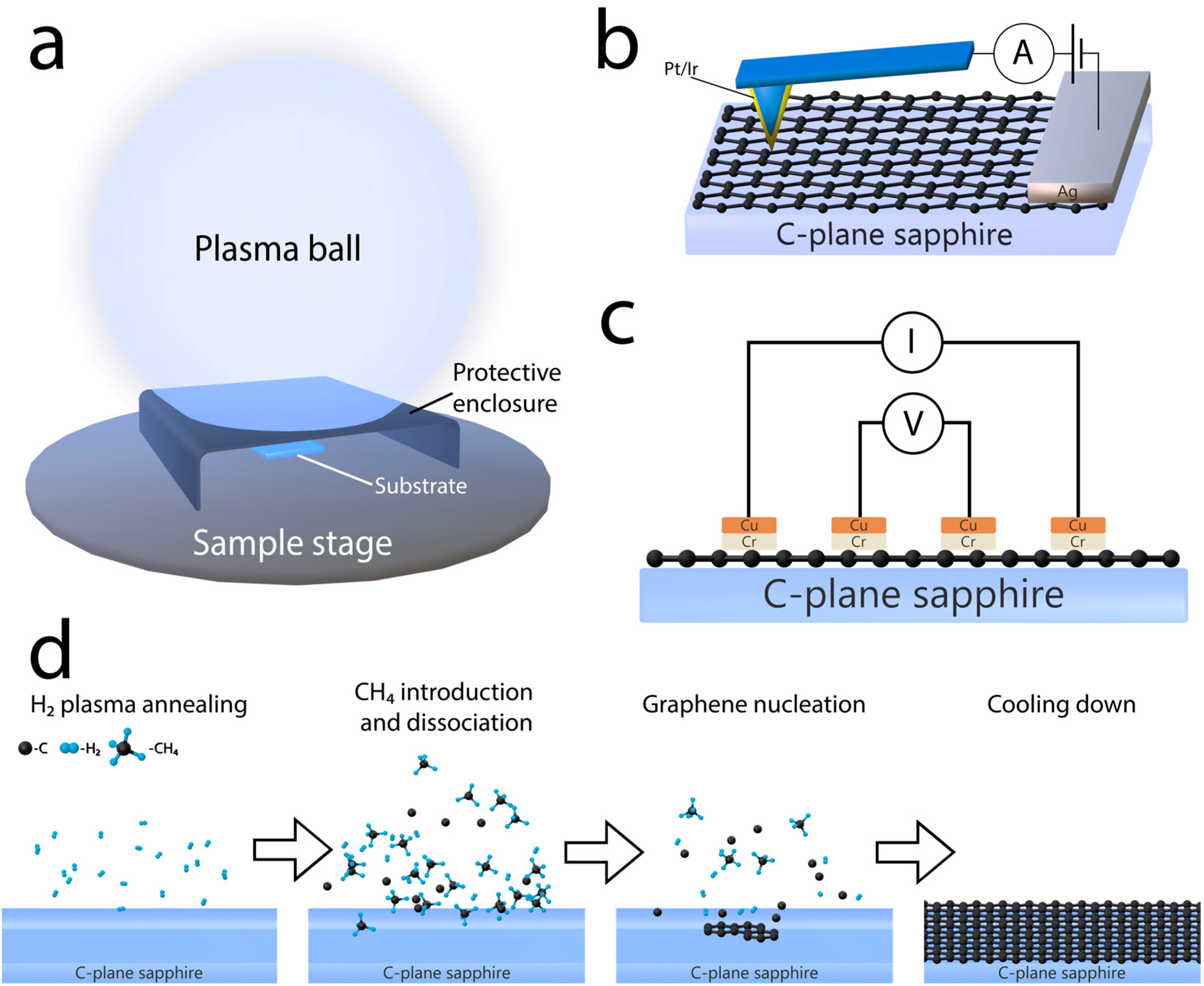
2. Materials and Methods
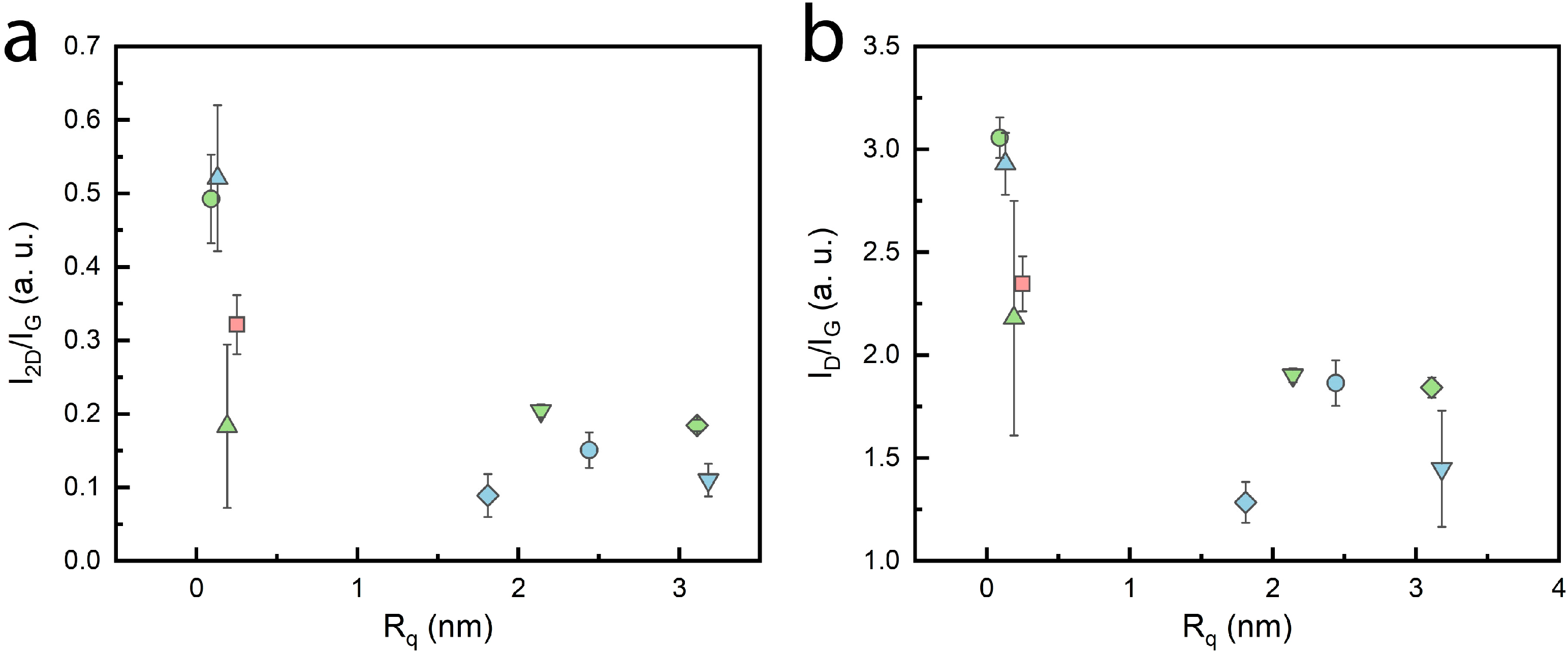
3. Results
4. Conclusions
Supplementary Materials
Author Contributions
Funding
Data Availability Statement
Acknowledgments
Conflicts of Interest
References
- Liao, L.; Lin, Y.-C.; Bao, M.; Cheng, R.; Bai, J.; Liu, Y.; Qu, Y.; Wang, K.L.; Huang, Y.; Duan, X. High-Speed Graphene Transistors with a Self-Aligned Nanowire Gate. Nature 2010, 467, 305–308. [Google Scholar] [CrossRef] [PubMed]
- Miao, X.; Tongay, S.; Petterson, M.K.; Berke, K.; Rinzler, A.G.; Appleton, B.R.; Hebard, A.F. High Efficiency Graphene Solar Cells by Chemical Doping. Nano Lett. 2012, 12, 2745–2750. [Google Scholar] [CrossRef]
- Xia, F.; Mueller, T.; Lin, Y.; Valdes-Garcia, A.; Avouris, P. Ultrafast Graphene Photodetector. Nat. Nanotechnol. 2009, 4, 839–843. [Google Scholar] [CrossRef]
- Davaji, B.; Cho, H.D.; Malakoutian, M.; Lee, J.-K.; Panin, G.; Kang, T.W.; Lee, C.H. A Patterned Single Layer Graphene Resistance Temperature Sensor. Sci. Rep. 2017, 7, 8811. [Google Scholar] [CrossRef]
- Zurauskiene, N.; Lukose, R.; Balevicius, S.; Stankevic, V.; Kersulis, S.; Plausinaitiene, V.; Vagner, M.; Navickas, R. Compact Manganite-Graphene Magnetoresistive Sensor. IEEE Magn. Lett. 2019, 10, 8105605. [Google Scholar] [CrossRef]
- Elgammal, K.; Hugosson, H.W.; Smith, A.D.; Råsander, M.; Bergqvist, L.; Delin, A. Density Functional Calculations of Graphene-Based Humidity and Carbon Dioxide Sensors: Effect of Silica and Sapphire Substrates. Surf. Sci. 2017, 663, 23–30. [Google Scholar] [CrossRef]
- Zhang, B.Y.; Liu, T.; Meng, B.; Li, X.; Liang, G.; Hu, X.; Wang, Q.J. Broadband High Photoresponse from Pure Monolayer Graphene Photodetector. Nat. Commun. 2013, 4, 1811. [Google Scholar] [CrossRef]
- Gan, X.; Shiue, R.-J.; Gao, Y.; Meric, I.; Heinz, T.F.; Shepard, K.; Hone, J.; Assefa, S.; Englund, D. Chip-Integrated Ultrafast Graphene Photodetector with High Responsivity. Nat. Photonics 2013, 7, 883–887. [Google Scholar] [CrossRef]
- Yi, M.; Shen, Z. A Review on Mechanical Exfoliation for the Scalable Production of Graphene. J. Mater. Chem. A Mater. 2015, 3, 11700–11715. [Google Scholar] [CrossRef]
- Coleman, J.N. Liquid Exfoliation of Defect-Free Graphene. Acc. Chem. Res. 2013, 46, 14–22. [Google Scholar] [CrossRef]
- Li, X.; Cai, W.; An, J.; Kim, S.; Nah, J.; Yang, D.; Piner, R.; Velamakanni, A.; Jung, I.; Tutuc, E.; et al. Large-Area Synthesis of High-Quality and Uniform Graphene Films on Copper Foils. Science 2009, 324, 1312–1314. [Google Scholar] [CrossRef] [PubMed]
- Deokar, G.; Avila, J.; Razado-Colambo, I.; Codron, J.-L.; Boyaval, C.; Galopin, E.; Asensio, M.-C.; Vignaud, D. Towards High Quality CVD Graphene Growth and Transfer. Carbon N. Y. 2015, 89, 82–92. [Google Scholar] [CrossRef]
- Deng, B.; Liu, Z.; Peng, H. Toward Mass Production of CVD Graphene Films. Adv. Mater. 2019, 31, e1800996. [Google Scholar] [CrossRef]
- Zhang, Y.; Zhang, L.; Zhou, C. Review of Chemical Vapor Deposition of Graphene and Related Applications. Acc. Chem. Res. 2013, 46, 2329–2339. [Google Scholar] [CrossRef]
- Losurdo, M.; Giangregorio, M.M.; Capezzuto, P.; Bruno, G. Graphene CVD Growth on Copper and Nickel: Role of Hydrogen in Kinetics and Structure. Phys. Chem. Chem. Phys. 2011, 13, 20836. [Google Scholar] [CrossRef] [PubMed]
- Gao, M.; Pan, Y.; Huang, L.; Hu, H.; Zhang, L.Z.; Guo, H.M.; Du, S.X.; Gao, H.-J. Epitaxial Growth and Structural Property of Graphene on Pt(111). Appl. Phys. Lett. 2011, 98, 033101. [Google Scholar] [CrossRef]
- Ullah, S.; Yang, X.; Ta, H.Q.; Hasan, M.; Bachmatiuk, A.; Tokarska, K.; Trzebicka, B.; Fu, L.; Rummeli, M.H. Graphene Transfer Methods: A Review. Nano Res. 2021, 14, 3756–3772. [Google Scholar] [CrossRef]
- Leong, W.S.; Wang, H.; Yeo, J.; Martin-Martinez, F.J.; Zubair, A.; Shen, P.-C.; Mao, Y.; Palacios, T.; Buehler, M.J.; Hong, J.-Y.; et al. Paraffin-Enabled Graphene Transfer. Nat. Commun. 2019, 10, 867. [Google Scholar] [CrossRef]
- Liang, X.; Sperling, B.A.; Calizo, I.; Cheng, G.; Hacker, C.A.; Zhang, Q.; Obeng, Y.; Yan, K.; Peng, H.; Li, Q.; et al. Toward Clean and Crackless Transfer of Graphene. ACS Nano 2011, 5, 9144–9153. [Google Scholar] [CrossRef]
- Haigh, S.J.; Gholinia, A.; Jalil, R.; Romani, S.; Britnell, L.; Elias, D.C.; Novoselov, K.S.; Ponomarenko, L.A.; Geim, A.K.; Gorbachev, R. Cross-Sectional Imaging of Individual Layers and Buried Interfaces of Graphene-Based Heterostructures and Superlattices. Nat. Mater. 2012, 11, 764–767. [Google Scholar] [CrossRef]
- Strupinski, W.; Grodecki, K.; Wysmolek, A.; Stepniewski, R.; Szkopek, T.; Gaskell, P.E.; Grüneis, A.; Haberer, D.; Bozek, R.; Krupka, J.; et al. Graphene Epitaxy by Chemical Vapor Deposition on SiC. Nano Lett. 2011, 11, 1786–1791. [Google Scholar] [CrossRef] [PubMed]
- Li, M.; Liu, D.; Wei, D.; Song, X.; Wei, D.; Wee, A.T.S. Controllable Synthesis of Graphene by Plasma-Enhanced Chemical Vapor Deposition and Its Related Applications. Adv. Sci. 2016, 3, 1600003. [Google Scholar] [CrossRef] [PubMed]
- Rehman, M.A.; Park, S.; Khan, M.F.; Bhopal, M.F.; Nazir, G.; Kim, M.; Farooq, A.; Ha, J.; Rehman, S.; Jun, S.C.; et al. Development of Directly Grown-graphene–Silicon Schottky Barrier Solar Cell Using Co-doping Technique. Int. J. Energy Res. 2022, 46, 11510–11522. [Google Scholar] [CrossRef]
- Kadam, K.D.; Rehman, M.A.; Kim, H.; Rehman, S.; Khan, M.A.; Patil, H.; Aziz, J.; Park, S.; Abdul Basit, M.; Khan, K.; et al. Enhanced and Passivated Co-Doping Effect of Organic Molecule and Bromine on Graphene/HfO2/Silicon Metal–Insulator–Semiconductor (MIS) Schottky Junction Solar Cells. ACS Appl. Energy Mater. 2022, 5, 10509–10517. [Google Scholar] [CrossRef]
- Meškinis, Š.; Vasiliauskas, A.; Guobienė, A.; Talaikis, M.; Niaura, G.; Gudaitis, R. The Direct Growth of Planar and Vertical Graphene on Si(100) via Microwave Plasma Chemical Vapor Deposition: Synthesis Conditions Effects. RSC Adv. 2022, 12, 18759–18772. [Google Scholar] [CrossRef]
- Rehman, M.A.; Roy, S.B.; Akhtar, I.; Bhopal, M.F.; Choi, W.; Nazir, G.; Khan, M.F.; Kumar, S.; Eom, J.; Chun, S.-H.; et al. Thickness-Dependent Efficiency of Directly Grown Graphene Based Solar Cells. Carbon N. Y. 2019, 148, 187–195. [Google Scholar] [CrossRef]
- Zhan, H.; Garrett, D.J.; Apollo, N.V.; Ganesan, K.; Lau, D.; Prawer, S.; Cervenka, J. Direct Fabrication of 3D Graphene on Nanoporous Anodic Alumina by Plasma-Enhanced Chemical Vapor Deposition. Sci. Rep. 2016, 6, 19822. [Google Scholar] [CrossRef]
- Park, J.; Lee, J.; Choi, J.-H.; Hwang, D.K.; Song, Y.-W. Growth, Quantitative Growth Analysis and Applications of Graphene on γ-Al2O3 Catalysts. Sci. Rep. 2015, 5, 11839. [Google Scholar] [CrossRef] [PubMed]
- Ueda, Y.; Maruyama, T.; Naritsuka, S. Effect of Growth Pressure on Graphene Direct Growth on an A-Plane Sapphire Substrate: Implications for Graphene-Based Electronic Devices. ACS Appl. Nano Mater. 2021, 4, 343–351. [Google Scholar] [CrossRef]
- Wördenweber, H.; Karthäuser, S.; Grundmann, A.; Wang, Z.; Aussen, S.; Kalisch, H.; Vescan, A.; Heuken, M.; Waser, R.; Hoffmann-Eifert, S. Atomically Resolved Electronic Properties in Single Layer Graphene on α-Al2O3 (0001) by Chemical Vapor Deposition. Sci. Rep. 2022, 12, 18743. [Google Scholar] [CrossRef]
- Chang, C.-J.; Tsai, P.-C.; Su, W.-Y.; Huang, C.-Y.; Lee, P.-T.; Lin, S.-Y. Layered Graphene Growth Directly on Sapphire Substrates for Applications. ACS Omega 2022, 7, 13128–13133. [Google Scholar] [CrossRef] [PubMed]
- Fanton, M.A.; Robinson, J.A.; Puls, C.; Liu, Y.; Hollander, M.J.; Weiland, B.E.; LaBella, M.; Trumbull, K.; Kasarda, R.; Howsare, C.; et al. Characterization of Graphene Films and Transistors Grown on Sapphire by Metal-Free Chemical Vapor Deposition. ACS Nano 2011, 5, 8062–8069. [Google Scholar] [CrossRef] [PubMed]
- Hwang, J.; Kim, M.; Campbell, D.; Alsalman, H.A.; Kwak, J.Y.; Shivaraman, S.; Woll, A.R.; Singh, A.K.; Hennig, R.G.; Gorantla, S.; et al. Van Der Waals Epitaxial Growth of Graphene on Sapphire by Chemical Vapor Deposition without a Metal Catalyst. ACS Nano 2013, 7, 385–395. [Google Scholar] [CrossRef] [PubMed]
- Li, J.; Chen, M.; Samad, A.; Dong, H.; Ray, A.; Zhang, J.; Jiang, X.; Schwingenschlögl, U.; Domke, J.; Chen, C.; et al. Wafer-Scale Single-Crystal Monolayer Graphene Grown on Sapphire Substrate. Nat. Mater. 2022, 21, 740–747. [Google Scholar] [CrossRef]
- Wang, G.; Zhao, Y.; Deng, Y.; Huang, W.; Fan, X.; Zhang, J.; Duan, R.; Sun, L. Lattice Selective Growth of Graphene on Sapphire Substrate. J. Phys. Chem. C 2015, 119, 426–430. [Google Scholar] [CrossRef]
- Chen, Z.; Xie, C.; Wang, W.; Zhao, J.; Liu, B.; Shan, J.; Wang, X.; Hong, M.; Lin, L.; Huang, L.; et al. Direct Growth of Wafer-Scale Highly Oriented Graphene on Sapphire. Sci. Adv. 2021, 7, eabk0115. [Google Scholar] [CrossRef]
- Chang, C.S.; Kim, K.S.; Park, B.-I.; Choi, J.; Kim, H.; Jeong, J.; Barone, M.; Parker, N.; Lee, S.; Zhang, X.; et al. Remote Epitaxial Interaction through Graphene. Sci. Adv. 2023, 9, eadj5379. [Google Scholar] [CrossRef]
- Mishra, N.; Forti, S.; Fabbri, F.; Martini, L.; McAleese, C.; Conran, B.R.; Whelan, P.R.; Shivayogimath, A.; Jessen, B.S.; Buß, L.; et al. Wafer-Scale Synthesis of Graphene on Sapphire: Toward Fab-Compatible Graphene. Small 2019, 15, e1904906. [Google Scholar] [CrossRef]
- Muñoz, R.; López-Elvira, E.; Munuera, C.; Carrascoso, F.; Xie, Y.; Çakıroğlu, O.; Pucher, T.; Puebla, S.; Castellanos-Gomez, A.; García-Hernández, M. Low T Direct Plasma Assisted Growth of Graphene on Sapphire and Its Integration in Graphene/MoS2 Heterostructure-Based Photodetectors. NPJ 2D Mater. Appl. 2023, 7, 57. [Google Scholar] [CrossRef]
- Wei, D.; Lu, Y.; Han, C.; Niu, T.; Chen, W.; Wee, A.T.S. Critical Crystal Growth of Graphene on Dielectric Substrates at Low Temperature for Electronic Devices. Angew. Chem. Int. Ed. 2013, 52, 14121–14126. [Google Scholar] [CrossRef]
- Lozano, M.S.; Bernat-Montoya, I.; Angelova, T.I.; Mojena, A.B.; Díaz-Fernández, F.J.; Kovylina, M.; Martínez, A.; Cienfuegos, E.P.; Gómez, V.J. Plasma-Induced Surface Modification of Sapphire and Its Influence on Graphene Grown by Plasma-Enhanced Chemical Vapour Deposition. Nanomaterials 2023, 13, 1952. [Google Scholar] [CrossRef] [PubMed]
- Jankauskas, Š.; Gudaitis, R.; Vasiliauskas, A.; Guobienė, A.; Meškinis, Š. The Graphene Structure’s Effects on the Current-Voltage and Photovoltaic Characteristics of Directly Synthesized Graphene/n-Si(100) Diodes. Nanomaterials 2022, 12, 1640. [Google Scholar] [CrossRef] [PubMed]
- Gudaitis, R.; Lazauskas, A.; Jankauskas, Š.; Meškinis, Š. Catalyst-Less and Transfer-Less Synthesis of Graphene on Si(100) Using Direct Microwave Plasma Enhanced Chemical Vapor Deposition and Protective Enclosures. Materials 2020, 13, 5630. [Google Scholar] [CrossRef] [PubMed]
- Merlen, A.; Buijnsters, J.; Pardanaud, C. A Guide to and Review of the Use of Multiwavelength Raman Spectroscopy for Characterizing Defective Aromatic Carbon Solids: From Graphene to Amorphous Carbons. Coatings 2017, 7, 153. [Google Scholar] [CrossRef]
- Malard, L.M.; Pimenta, M.A.; Dresselhaus, G.; Dresselhaus, M.S. Raman Spectroscopy in Graphene. Phys. Rep. 2009, 473, 51–87. [Google Scholar] [CrossRef]
- Childres, I.; Jauregui, L.A.; Tian, J.; Chen, Y.P. Effect of Oxygen Plasma Etching on Graphene Studied Using Raman Spectroscopy and Electronic Transport Measurements. New J. Phys. 2011, 13, 025008. [Google Scholar] [CrossRef]
- Hwang, J.-S.; Lin, Y.-H.; Hwang, J.-Y.; Chang, R.; Chattopadhyay, S.; Chen, C.-J.; Chen, P.; Chiang, H.-P.; Tsai, T.-R.; Chen, L.-C.; et al. Imaging Layer Number and Stacking Order through Formulating Raman Fingerprints Obtained from Hexagonal Single Crystals of Few Layer Graphene. Nanotechnology 2013, 24, 015702. [Google Scholar] [CrossRef]
- Casiraghi, C.; Pisana, S.; Novoselov, K.S.; Geim, A.K.; Ferrari, A.C. Raman Fingerprint of Charged Impurities in Graphene. Appl. Phys. Lett. 2007, 91, 233108. [Google Scholar] [CrossRef]
- Meškinis, Š.; Gudaitis, R.; Vasiliauskas, A.; Guobienė, A.; Jankauskas, Š.; Stankevič, V.; Keršulis, S.; Stirkė, A.; Andriukonis, E.; Melo, W.; et al. Biosensor Based on Graphene Directly Grown by MW-PECVD for Detection of COVID-19 Spike (S) Protein and Its Entry Receptor ACE2. Nanomaterials 2023, 13, 2373. [Google Scholar] [CrossRef]
- Song, H.J.; Son, M.; Park, C.; Lim, H.; Levendorf, M.P.; Tsen, A.W.; Park, J.; Choi, H.C. Large Scale Metal-Free Synthesis of Graphene on Sapphire and Transfer-Free Device Fabrication. Nanoscale 2012, 4, 3050. [Google Scholar] [CrossRef]
- Zheng, S.; Zhong, G.; Wu, X.; D’Arsiè, L.; Robertson, J. Metal-Catalyst-Free Growth of Graphene on Insulating Substrates by Ammonia-Assisted Microwave Plasma-Enhanced Chemical Vapor Deposition. RSC Adv. 2017, 7, 33185–33193. [Google Scholar] [CrossRef]
- Kim, Y.S.; Joo, K.; Jerng, S.-K.; Lee, J.H.; Yoon, E.; Chun, S.-H. Direct Growth of Patterned Graphene on SiO 2 Substrates without the Use of Catalysts or Lithography. Nanoscale 2014, 6, 10100–10105. [Google Scholar] [CrossRef] [PubMed]
- Vishwakarma, R.; Rosmi, M.S.; Takahashi, K.; Wakamatsu, Y.; Yaakob, Y.; Araby, M.I.; Kalita, G.; Kitazawa, M.; Tanemura, M. Transfer Free Graphene Growth on SiO2 Substrate at 250 °C. Sci. Rep. 2017, 7, 43756. [Google Scholar] [CrossRef] [PubMed]
- Xu, S.C.; Man, B.Y.; Jiang, S.Z.; Chen, C.S.; Yang, C.; Liu, M.; Gao, X.G.; Sun, Z.C.; Zhang, C. Direct Synthesis of Graphene on SiO2 Substrates by Chemical Vapor Deposition. CrystEngComm 2013, 15, 1840. [Google Scholar] [CrossRef]
- Gupta, A.; Chen, G.; Joshi, P.; Tadigadapa, S. Eklund Raman Scattering from High-Frequency Phonons in Supported n-Graphene Layer Films. Nano Lett. 2006, 6, 2667–2673. [Google Scholar] [CrossRef] [PubMed]
- Cho, J.H.; Gorman, J.J.; Na, S.R.; Cullinan, M. Growth of Monolayer Graphene on Nanoscale Copper-Nickel Alloy Thin Films. Carbon N. Y. 2017, 115, 441–448. [Google Scholar] [CrossRef]
- Ferrari, A.C.; Basko, D.M. Raman Spectroscopy as a Versatile Tool for Studying the Properties of Graphene. Nat. Nanotechnol. 2013, 8, 235–246. [Google Scholar] [CrossRef]
- Eckmann, A.; Felten, A.; Mishchenko, A.; Britnell, L.; Krupke, R.; Novoselov, K.S.; Casiraghi, C. Probing the Nature of Defects in Graphene by Raman Spectroscopy. Nano Lett. 2012, 12, 3925–3930. [Google Scholar] [CrossRef]
- Venezuela, P.; Lazzeri, M.; Mauri, F. Theory of Double-Resonant Raman Spectra in Graphene: Intensity and Line Shape of Defect-Induced and Two-Phonon Bands. Phys. Rev. B 2011, 84, 035433. [Google Scholar] [CrossRef]
- Ni, Z.H.; Yu, T.; Lu, Y.H.; Wang, Y.Y.; Feng, Y.P.; Shen, Z.X. Uniaxial Strain on Graphene: Raman Spectroscopy Study and Band-Gap Opening. ACS Nano 2008, 2, 2301–2305. [Google Scholar] [CrossRef]
- Yoon, D.; Son, Y.-W.; Cheong, H. Negative Thermal Expansion Coefficient of Graphene Measured by Raman Spectroscopy. Nano Lett. 2011, 11, 3227–3231. [Google Scholar] [CrossRef] [PubMed]
- Neumann, C.; Reichardt, S.; Venezuela, P.; Drögeler, M.; Banszerus, L.; Schmitz, M.; Watanabe, K.; Taniguchi, T.; Mauri, F.; Beschoten, B.; et al. Raman Spectroscopy as Probe of Nanometre-Scale Strain Variations in Graphene. Nat. Commun. 2015, 6, 8429. [Google Scholar] [CrossRef]
- Ni, Z.; Wang, Y.; Yu, T.; You, Y.; Shen, Z. Reduction of Fermi Velocity in Folded Graphene Observed by Resonance Raman Spectroscopy. Phys. Rev. B 2008, 77, 235403. [Google Scholar] [CrossRef]
- Ferrari, A.C.; Meyer, J.C.; Scardaci, V.; Casiraghi, C.; Lazzeri, M.; Mauri, F.; Piscanec, S.; Jiang, D.; Novoselov, K.S.; Roth, S.; et al. Raman Spectrum of Graphene and Graphene Layers. Phys. Rev. Lett. 2006, 97, 187401. [Google Scholar] [CrossRef]
- Lee, J.E.; Ahn, G.; Shim, J.; Lee, Y.S.; Ryu, S. Optical Separation of Mechanical Strain from Charge Doping in Graphene. Nat. Commun. 2012, 3, 1024. [Google Scholar] [CrossRef] [PubMed]
- Kim, S.; Ryu, S. Thickness-Dependent Native Strain in Graphene Membranes Visualized by Raman Spectroscopy. Carbon N. Y. 2016, 100, 283–290. [Google Scholar] [CrossRef]
- Morozov, S.V.; Novoselov, K.S.; Katsnelson, M.I.; Schedin, F.; Elias, D.C.; Jaszczak, J.A.; Geim, A.K. Giant Intrinsic Carrier Mobilities in Graphene and Its Bilayer. Phys. Rev. Lett. 2008, 100, 016602. [Google Scholar] [CrossRef]
- Yang, W.; He, C.; Zhang, L.; Wang, Y.; Shi, Z.; Cheng, M.; Xie, G.; Wang, D.; Yang, R.; Shi, D.; et al. Growth, Characterization, and Properties of Nanographene. Small 2012, 8, 1429–1435. [Google Scholar] [CrossRef]
- Zhang, H.; Lee, G.; Gong, C.; Colombo, L.; Cho, K. Grain Boundary Effect on Electrical Transport Properties of Graphene. J. Phys. Chem. C 2014, 118, 2338–2343. [Google Scholar] [CrossRef]


| Set | Sample No. | Power, kW | H2, sccm | CH4, sccm | p, mBar | T, °C | t, min. |
|---|---|---|---|---|---|---|---|
| F1 | 0.7 | 75 | 25 | 10 | 700 | 60 | |
| F2 | 0.7 | 70 | 30 | 10 | 700 | 60 | |
| F | F3P2 | 0.7 | 65 | 35 | 10 | 700 | 60 |
| F4 | 0.7 | 60 | 40 | 10 | 700 | 60 | |
| F5 | 0.7 | 55 | 45 | 10 | 700 | 60 | |
| P1 | 0.7 | 65 | 35 | 6 | 700 | 60 | |
| F3P2 | 0.7 | 65 | 35 | 10 | 700 | 60 | |
| P | P3 | 0.7 | 65 | 35 | 15 | 700 | 60 |
| P4 | 0.7 | 65 | 35 | 20 | 700 | 60 | |
| P5 | 0.7 | 65 | 35 | 25 | 700 | 60 | |
| S1 | 0.7 | 80 | 20 | 6 | 700 | 60 | |
| S | S2 | 0.7 | 75 | 25 | 6 | 700 | 60 |
| S3 | 0.7 | 75 | 25 | 25 | 700 | 60 |
| Sample No. | Highest Surface Point, nm | Sheet Resistance, kΩ/□ | Reference |
|---|---|---|---|
| A-plane sapphire | Low-pressure CVD | 0.728 | [29] |
| C-plane sapphire | Electron cyclotron resonance CVD | 0.95 | [39] |
| C-plane sapphire | High-temperature CVD | ~1 | [32] |
| Sapphire | Critical PECVD | 4.1 | [40] |
| C-plane sapphire | PECVD | 1.87 | This study |
Disclaimer/Publisher’s Note: The statements, opinions and data contained in all publications are solely those of the individual author(s) and contributor(s) and not of MDPI and/or the editor(s). MDPI and/or the editor(s) disclaim responsibility for any injury to people or property resulting from any ideas, methods, instructions or products referred to in the content. |
© 2024 by the authors. Licensee MDPI, Basel, Switzerland. This article is an open access article distributed under the terms and conditions of the Creative Commons Attribution (CC BY) license (https://creativecommons.org/licenses/by/4.0/).
Share and Cite
Jankauskas, Š.; Meškinis, Š.; Žurauskienė, N.; Guobienė, A. Influence of Synthesis Parameters on Structure and Characteristics of the Graphene Grown Using PECVD on Sapphire Substrate. Nanomaterials 2024, 14, 1635. https://doi.org/10.3390/nano14201635
Jankauskas Š, Meškinis Š, Žurauskienė N, Guobienė A. Influence of Synthesis Parameters on Structure and Characteristics of the Graphene Grown Using PECVD on Sapphire Substrate. Nanomaterials. 2024; 14(20):1635. https://doi.org/10.3390/nano14201635
Chicago/Turabian StyleJankauskas, Šarūnas, Šarūnas Meškinis, Nerija Žurauskienė, and Asta Guobienė. 2024. "Influence of Synthesis Parameters on Structure and Characteristics of the Graphene Grown Using PECVD on Sapphire Substrate" Nanomaterials 14, no. 20: 1635. https://doi.org/10.3390/nano14201635
APA StyleJankauskas, Š., Meškinis, Š., Žurauskienė, N., & Guobienė, A. (2024). Influence of Synthesis Parameters on Structure and Characteristics of the Graphene Grown Using PECVD on Sapphire Substrate. Nanomaterials, 14(20), 1635. https://doi.org/10.3390/nano14201635