Communication

Read Operation Mechanism of Feedback Field-Effect Transistors with Quasi-Nonvolatile Memory States

Department of Electrical Engineering, Korea University, 145 Anam-ro, Seongbuk-gu, Seoul 02841, Republic of Korea
*
Authors to whom correspondence should be addressed.
Nanomaterials 2024, 14(2), 210; https://doi.org/10.3390/nano14020210
Submission received: 26 December 2023 / Revised: 16 January 2024 / Accepted: 17 January 2024 / Published: 18 January 2024
(This article belongs to the Special Issue Semiconductor Nanomaterials for Memory Devices)

Abstract

:
In this study, the read operation of feedback field-effect transistors (FBFETs) with quasi-nonvolatile memory states was analyzed using a device simulator. For FBFETs, write pulses of 40 ns formed potential barriers in their channels, and charge carriers were accumulated (depleted) in these channels, generating the memory state “State 1 (State 0)”. Read pulses of 40 ns read these states with a retention time of 3 s, and the potential barrier formation and carrier accumulation were influenced by these read pulses. The potential barriers were analyzed, using junction voltage and current density to explore the memory states. Moreover, FBFETs exhibited nondestructive readout characteristics during the read operation, which depended on the read voltage and pulse width.

1. Introduction

Quasi-nonvolatile memory has been developed as a novel memory technology. Its retention time ranges from 64 ms to 10 years, which is the gap between volatile and nonvolatile memories [1]. The ability to store data without a power supply reduces power consumption [2,3]. This type of memory addresses the timescale gap in the memory hierarchy. Traditional memory has evolved to satisfy the demands of high-performance computing [4,5]. Volatile memory, such as static or dynamic random-access memory, offers an ultrahigh speed with a limited retention time [6,7,8]. Nonvolatile memory, such as NAND flash memory, provides a retention time of 10 years but exhibits a low operation speed [6,9]. With the current data-centric trend, a timescale gap in the memory hierarchy worsens memory bottlenecks [10,11]. Recent studies have demonstrated the potential of quasi-nonvolatile memory; however, improvements are still required [12,13]. To replace traditional memory successfully, the new memory must possess unlimited write/read cycles. Feedback field-effect transistors (FBFETs) have emerged as attractive candidates for quasi-nonvolatile memory owing to their fast write/read speeds, long retention times, and nondestructive readout characteristics [3]. Furthermore, their inherent operating mechanism ensures high endurance, and their compatibility with complementary metal–oxide–semiconductor (CMOS) technology indicates that they can potentially replace traditional memory fully [3,14].
In FBFETs, the positive feedback mechanism enables quasi-nonvolatile memory operations. Their memory states are defined by the presence (State 1) and absence (State 0) of excess charge carriers in the channels. When the potential barriers collapse (form) abruptly due to the accumulation (depletion) of excess charge carriers, the positive feedback loop is activated (eliminated) in their channels, and their memory state becomes State 1 (State 0) [15,16]. Consequently, State 1 (State 0) is perceived by reading the high (low) current. The speed and pulse configuration of the reading influence the formation of the potential barrier [17,18,19]; thus, the readout characteristics depend on the read pulse. Understanding the read mechanism is crucial for further enhancing quasi-nonvolatile characteristics. In this study, the read operation of FBFETs with quasi-nonvolatile memory states was analyzed using technology computer-aided design (TCAD) simulation. The read operation of the FBFETs was newly interpreted via the analysis of a positive feedback mechanism at a nanosecond-order speed. Junction voltage and current density analysis were employed to examine the carrier type predominantly influencing the formation of the positive feedback loop and the role of channel potential barriers during the read operation. This study provides valuable insight into optimizing the FBFET design for performance enhancement and suggests the potential for achieving ultra-high-speed operation through a new reading scheme.

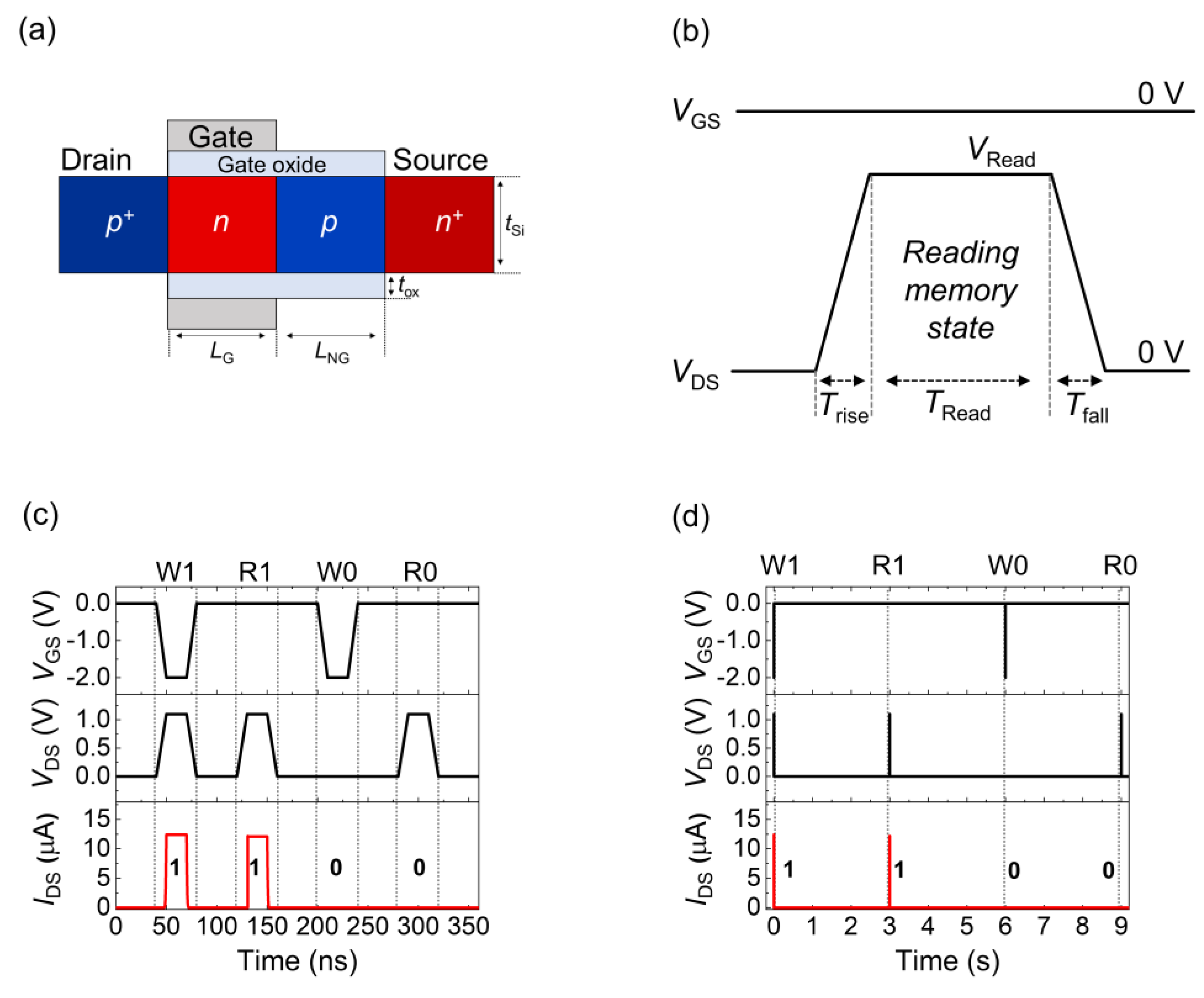
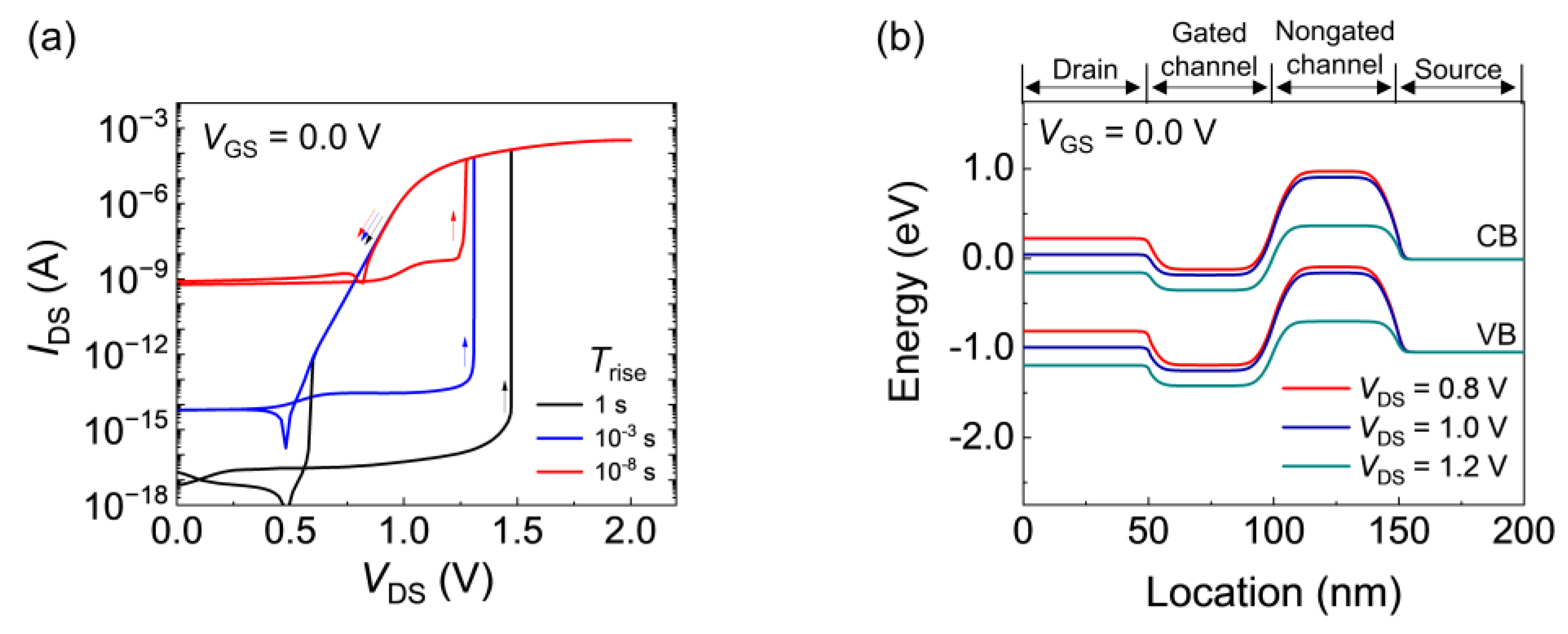
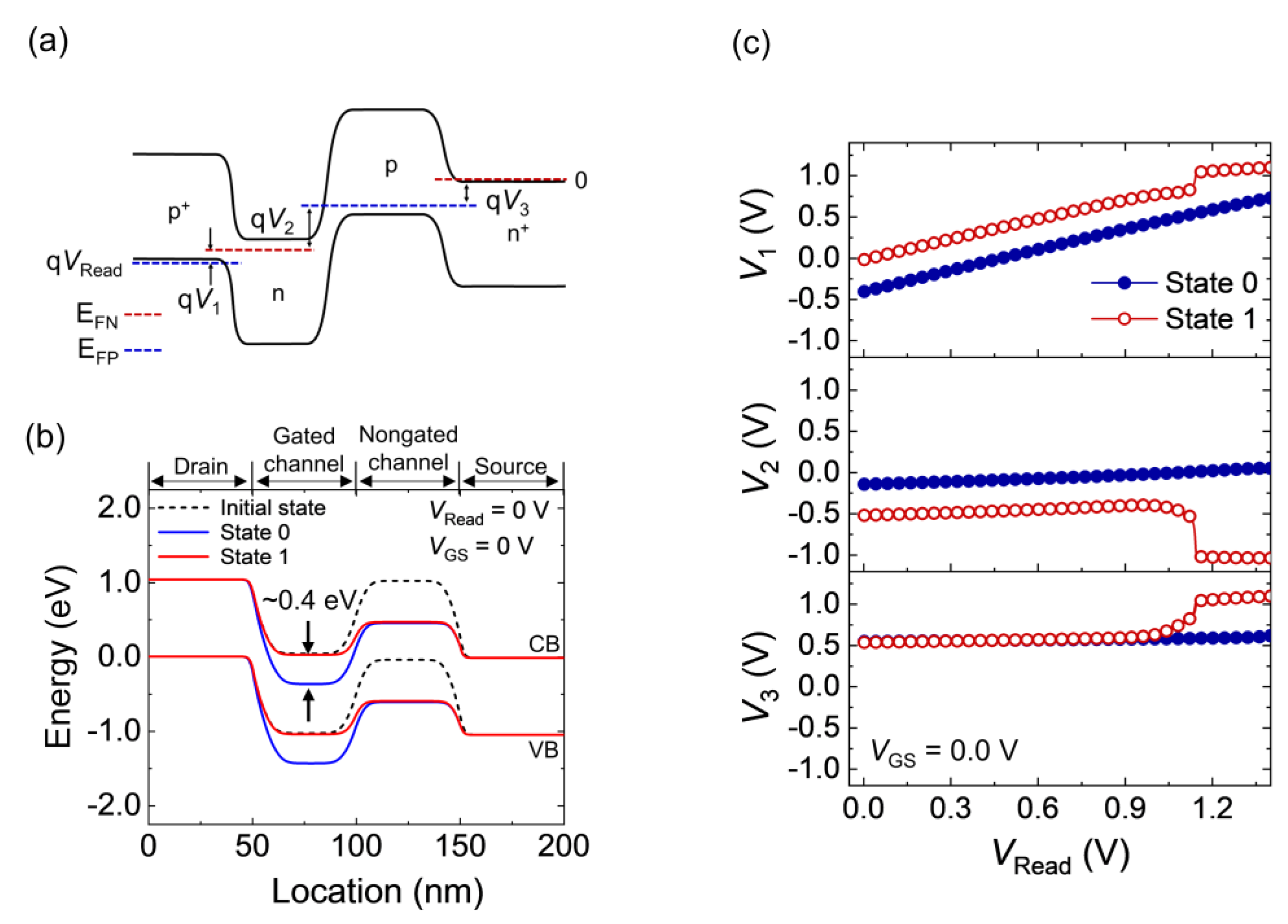
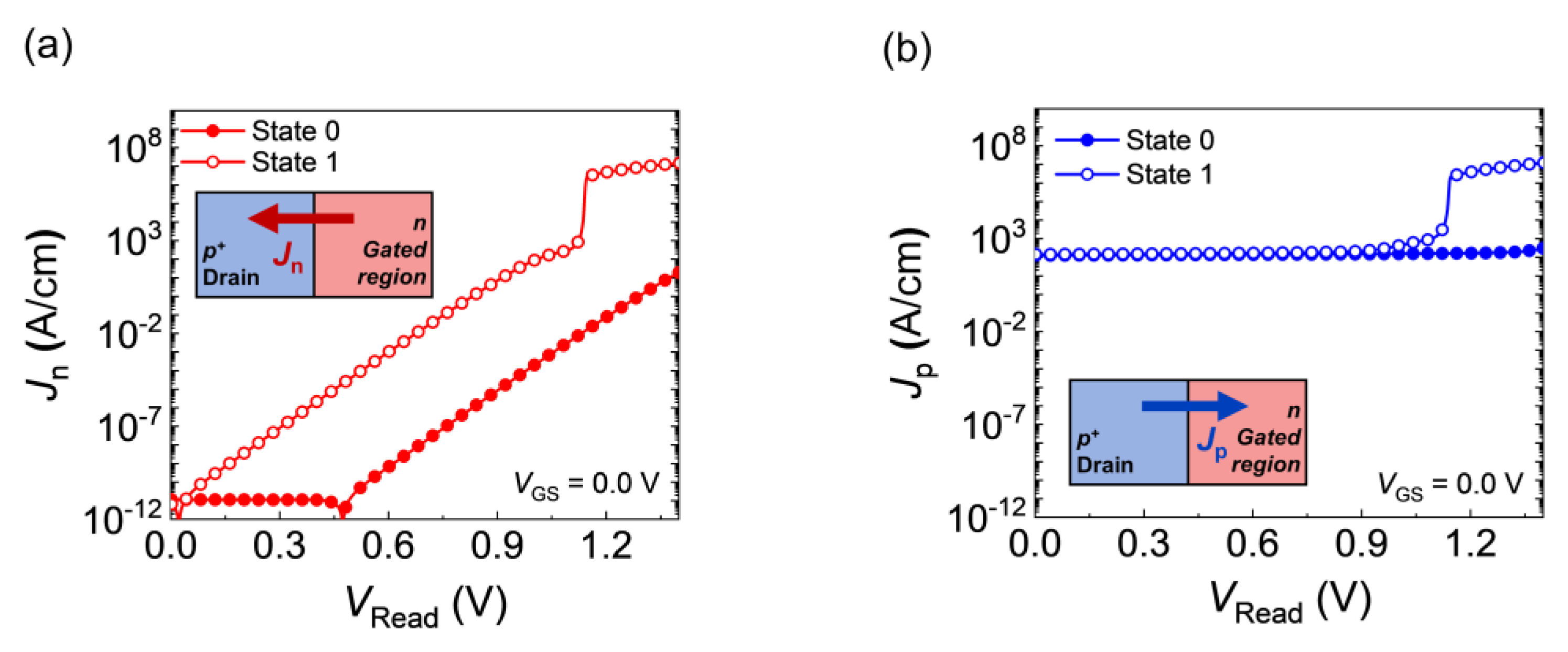
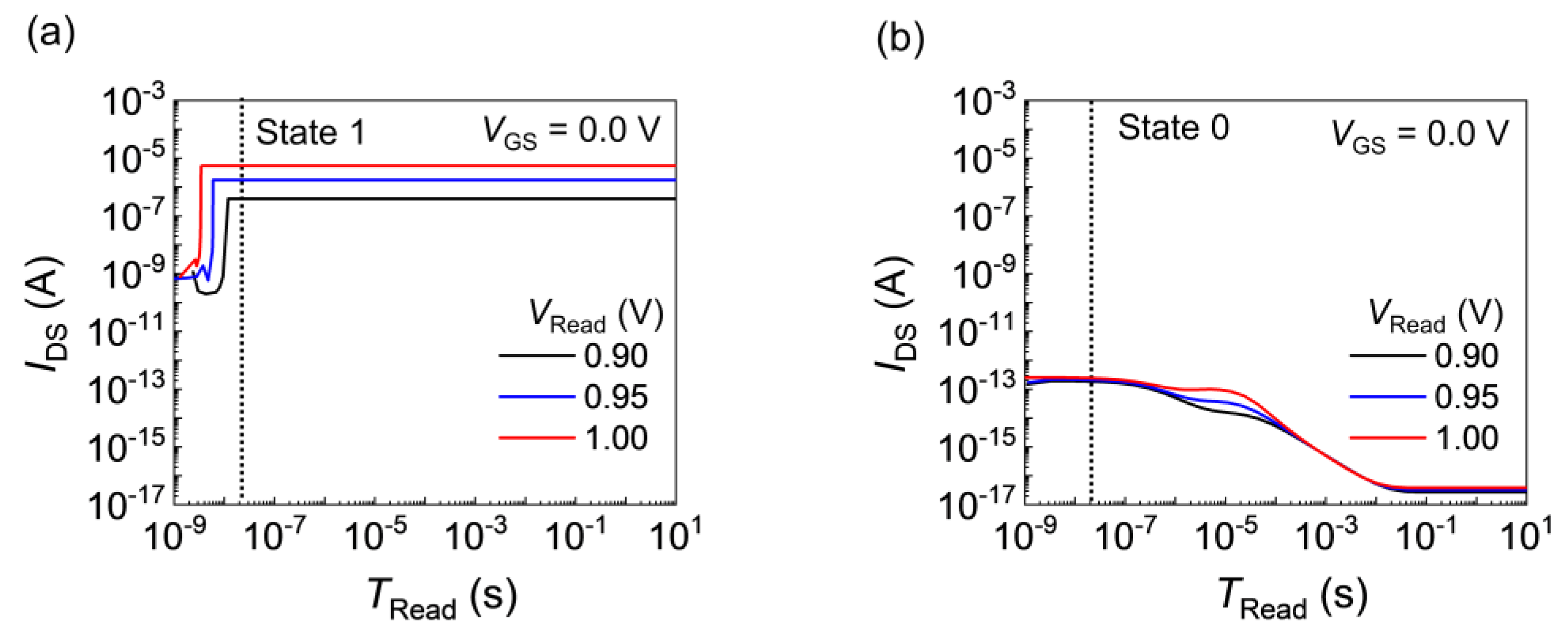
2. Results and Discussions

Figure 1a shows a schematic of a representative FBFET with a p-n-p-n structure. The dimensional parameters were a gated channel length (LG) of 50 nm, a nongated channel length (LNG) of 50 nm, a channel thickness (tSi) of 20 nm, and a gate oxide SiO2 thickness (tox) of 5 nm. The doping concentrations were 3 × 1019 cm−3 for the source and drain regions and 5 × 1018 cm−3 for the gated and nongated channel regions. The gate, drain, and source electrodes were made of aluminum (work function = 4.0 eV). These parameters are summarized in Table 1. Figure 1b shows a schematic of a VDS pulse (with VGS = 0 V) for reading quasi-nonvolatile memory states. During the read operation, VDS increased to the reading voltage (VRead) within the rising time (Trise) and fell to 0 V during the falling time (Tfall), the Tfall value was the same as the Trise value. Memory states were verified by measuring the drain-to-source current (IDS) during the reading time (TRead). The quasi-nonvolatile memory operation is depicted in Figure 1c, where the Trise and TRead values were 10 and 20 ns, respectively. The sequence Write 1-Read-Write 0-Read was performed to verify the memory states. After the write operation, the IDS values were ~12 μA and 3.8 pA for States 1 and 0, respectively. Moreover, the retention time was 3 s, as observed in the full memory cycle (Figure 1d).
Figure 2 shows the output characteristics (a) and band diagram (b) of the FBFETs. For the Trise values of 1, 10−3, and 10−8 s, the FBFETs exhibited bistable characteristics (in the forward and reverse drain-to-source voltage (VDS) sweeps) caused by the positive feedback loop associated with the potential barrier and carrier accumulation in the channel. A positive feedback loop was activated when the repeated accumulation of excess carriers collapsed the potential barrier in the channel. For a Trise of 1 s, the IDS abruptly increased at a VDS of 1.47 V in the sweep of VDS from 0 to 2.0 V, which was the latch-up phenomenon. For a Trise shorter than 1 s, the formation of the potential barrier was hindered sufficiently to block the carrier flow; for a Trise of 10−8 s, the potential barrier in the gated channel decreased as VDS increased (Figure 2b). Consequently, the latch-up voltage decreased from 1.47 to 1.26 V and the transient leakage current increased from ~10−16 to ~10−9 A as Trise decreased from 1 to 10−8 s.
The formation of the potential barrier affects each p-n junction of the FBFETs during the read operation. As shown in Figure 3a, the junction voltages (V1, V2, and V3) are defined as the differences between the electron and hole quasi-Fermi levels (EFN and EFP, respectively). Note that the positive V2 was the reverse bias to the center junction; the equation VRead = V1 + V2 + V3 was established before the latch-up [20]. The junction voltages indicated the potential barrier heights of the channels. The accumulation (depletion) of charge carriers in the channels generated a memory state: State 1 (State 0). The accumulation and depletion of charge carriers are described in detail in the supplementary information. The potential barrier in the gated channel was higher by 0.4 eV in State 0 than in State 1 (Figure 3b). Thus, at VRead = 0 V, the initial values of V1 and V2 differed by 0.40 V between States 1 and 0, which corresponded to the difference in the potential barrier in the gated channel. As VRead w\s swept for a Trise of 10 ns (Figure 3c), V1 and V2 sustained the difference between States 1 and 0 during the VRead sweep, whereas V3 was the same for States 1 and 0 before latch-up. The sustained potential barrier induced a difference between States 1 and 0. As VRead reached 1.05 V, V1 and V3 increased, and V2 decreased abruptly in State 1. These results indicate that the potential barrier collapsed at 1.05 V in State 1 but not in State 0. V1 accounted for most of VRead in both states. An increase in V1 signified an increase in the forward bias applied to the drain-side p-n junction. Therefore, the collapse of the channel potential barrier in State 1 arose from the unintended carrier flow at the drain-side p-n junction.
When a positive VDS was applied to the FBFETs, electrons flowed toward the drain, whereas holes flowed toward the source. Some electrons injected from the source accumulated in the potential well, whereas the rest passed through the channel. Thus, the electron current density (Jn) at the drain-side p-n junction represents the electrons that pass through, which are related to the increase in the V1 value. In contrast, the hole current density (Jp) at the drain-side p-n junction refers to hole injection from the drain. The number of injected holes is equal to the sum of the numbers of holes that are accumulated, recombined (or generated), and passed through. Jn and Jp at the drain-side p-n junction are plotted as functions of VDS in Figure 4. For a Trise of 10 ns, as VRead increased to 2.00 V, Jn instantly increased in State 1, whereas it remained at 10−11 A/cm in State 0 until a VRead of 0.42 V (Figure 4a). However, Jp remained at ~102 A/cm before the latch-up in both memory states (Figure 4b). As Jn reached the same magnitude as Jp (~102 A/cm), Jp increased and eventually led to a latch-up; the increase in Jn induced the collapse of the channel potential barrier. As the Jn curve in State 0 was shifted rightward by 0.42 V compared with State 1, the latch-up phenomenon occurred at VRead = 1.05 V for State 1, whereas it did not for State 0. The results showed that the flow of electrons in the channel influenced the activation of the positive feedback loop. In State 0, the higher potential barrier in the gated channel inhibited the flow of electrons, resulting in a difference from State 1.
Figure 5 shows the IDS response to the read operation for various VRead values in States 1 and 0 with a Trise of 10 ns. The IDS value indicates the memory state during TRead. Accordingly, the moderate VRead range depends on the selection of TRead. For TRead = 20 ns, marked with dotted lines in the figure, States 1 and 0 exhibited distinct IDS results during the read operation. As shown in Figure 5a, as VRead decreased to 0.90 V, the positive feedback loop activation was delayed in State 1. However, even if VRead was less than the latch-up voltage, the positive feedback loop was activated in State 1. In Figure 5b, for State 0, the IDS values stabilized at ~10−16 A over time. The carrier flows were hindered by the potential barrier in State 0 during VRead; thus, the FBFETs exhibited nondestructive readout characteristics.
An investigation of the read operation is necessary to improve the reading speed of quasi-nonvolatile memory states. The memory window, namely, the VRead range for recognizing memory states, is not exclusively defined by the DC characteristics of the FBFETs. At nanosecond-order speeds, the flow of charge carriers in the channel influences the activation of a positive feedback loop. To enhance the current-sensing margin, the reinforcement of the gated channel barrier is required to suppress the carriers passing through and reduce the leakage current. In State 1, charge carriers are accumulated in the gated channel after the read operation, which reduces the activation time of the positive feedback loop for the subsequent read operation. In State 0, owing to the high-potential barrier, charge carriers remain depleted in the gated channel after the read operation (for more details, see the Supplementary Information). The nondestructive readout characteristics enable stable and recursive read operations [21]. Therefore, incorporating the initialized operation into the read pulse scheme allows FBFETs to operate at an SRAM-like speed (sub-1 ns). Moreover, applying a flexible pulse scheme during repetitive read operations can improve the performance of FBFETs. Consequently, a suitable tool can be designed for a specific purpose through an in-depth understanding of the reading operation of FBFETs.

3. Conclusions

The read operations of FBFETs were investigated with quasi-nonvolatile memory states. FBFETs exhibited a retention time of 3 s for write and read pulses of 40 ns. State 1 (State 0) was generated by the accumulation (depletion) of charge carriers in the channels. During the rise in VRead at a Trise of 10 ns, the increase in electron flow at the drain-side p-n junction affected the activation of the positive feedback loop in the channel. In State 1, as Jn reached the same magnitude as Jp (~102 A/cm), the potential barrier collapsed at a VRead of 1.05 V, which caused a latch-up. In State 0, the high-potential barrier in the gated channel inhibited the flow of electrons, which differed from State 1. Consequently, the read operation was distinguishable for States 1 and 0 with nondestructive characteristics. Moreover, the range of VRead depended on the pulse width during the read operation. The results provided insights for improving the performance of FBFETs as quasi-nonvolatile memory devices.

4. Simulation Method

The simulation was performed with a two-dimensional structure using the commercial device simulator Synopsys Sentaurus (O_2018.06) [22]. The Lombardi, Philips unified mobility, and high-field saturation models were used to consider the doping and field dependencies of carrier mobility. The Fermi statistics were used to perform an accurate simulation. Also, bandgap narrowing (Slotboom model), band-to-band tunneling, Shockley–Read–Hall (SRH) recombination with concentration-dependent lifetimes, surface SRH recombination, and Auger recombination were considered. Furthermore, an area factor of 20 nm was specified in the simulation to determine the device width.

Supplementary Materials

The following supporting information can be downloaded at: https://www.mdpi.com/article/10.3390/nano14020210/s1, Figure S1. (a) Electron and (b) hole distributions in States 0 and 1. (c) Electron and (d) hole concentrations in States 0 and 1 at the 1 nm position below the gate oxide. Figure S2. (a) Electron and (b) hole distributions in States 0 and 1 before and after the read operation.

Author Contributions

Conceptualization, J.J., K.C. and S.K.; Methodology, J.J., K.C. and S.K.; Validation, J.J. and K.C.; Formal Analysis, J.J.; Investigation, J.J. and K.C.; Writing—Original Draft Preparation, J.J.; Writing—Review & Editing, K.C. and S.K.; Visualization J.J., K.C. and S.K.; Supervision, S.K.; Funding Acquisition, S.K. All authors have read and agreed to the published version of the manuscript.

Funding

This study was funded by a National Research Foundation of Korea (NRF) grant funded by the Korean government (MSIT) (2020R1A2C3004538, 2022M3I7A3046571, RS-2023-00260876), the Brain Korea 21 Plus Project through the NRF funded by the Ministry of Science, ICT & Future Planning, Samsung Electronics (IO201223-08257-01), and a Korea University Grant.

Data Availability Statement

Data are contained within the article.

Conflicts of Interest

The authors declare no conflicts of interest.

References

  1. Liu, C.; Yan, X.; Song, X.; Ding, S.; Zhang, D.W.; Zhou, P. A semi-floating gate memory based on van der Waals heterostructures for quasi-non-volatile applications. Nat. Nanotechnol. 2018, 13, 404–410. [Google Scholar] [CrossRef]
  2. Yang, K.; Liu, H.; Wang, S.; Yu, W.; Han, T. Comprehensive performance quasi-non-volatile memory compatible with large-scale preparation by chemical vapor deposition. Nanomaterials 2020, 10, 1471. [Google Scholar] [CrossRef] [PubMed]
  3. Lim, D.; Son, J.; Cho, K.; Kim, S. Quasi-nonvolatile silicon memory device. Adv. Mater. Technol. 2020, 5, 2000915. [Google Scholar] [CrossRef]
  4. Wong, H.S.; Salahuddin, S. Memory leads the way to better computing. Nat. Nanotechnol. 2015, 10, 191–194. [Google Scholar] [CrossRef] [PubMed]
  5. Lee, S.-H. Technology scaling challenges and opportunities of memory devices. In Proceedings of the IEEE International Electron Devices Meeting (IEDM), San Francisco, CA, USA, 3–7 December 2016; IEEE Publications: New York, NY, USA, 2016; Volume 2016, pp. 1.1.1–1.1.8. [Google Scholar] [CrossRef]
  6. Yu, S.; Chen, P. Emerging Memory Technologies: Recent Trends and Prospects. IEEE Solid State Circuits Mag. 2016, 8, 43–56. [Google Scholar] [CrossRef]
  7. Spessot, A.; Oh, H. 1T-1C dynamic random access memory status, challenges, and prospects. IEEE Trans. Electron. Devices 2020, 67, 1382–1393. [Google Scholar] [CrossRef]
  8. Park, J.M.; Hwang, Y.S.; Kim, S.-W.; Han, S.Y.; Park, J.S.; Kim, J.; Seo, J.W.; Kim, B.S.; Shin, S.H.; Cho, C.H.; et al. 20nm DRAM: A new beginning of another revolution. In Proceedings of the 2015 IEEE International Electron Devices Meeting (IEDM), Washington, DC, USA, 7–9 December 2015; pp. 26.5.1–26.5.4. [Google Scholar] [CrossRef]
  9. Cao, Q.; Lü, W.; Wang, X.R.; Guan, X.; Wang, L.; Yan, S.; Wu, T.; Wang, X. Nonvolatile multistates memories for high-density data storage. ACS Appl. Mater. Interfaces 2020, 12, 42449–42471. [Google Scholar] [CrossRef] [PubMed]
  10. Hwang, C.S. Prospective of semiconductor memory devices: From memory system to materials. Adv. Electron. Mater. 2015, 1, 1400056. [Google Scholar] [CrossRef]
  11. Ielmini, D.; Wong, H.-S.P. In-memory computing with resistive switching devices. Nat. Electron. 2018, 1, 333–343. [Google Scholar] [CrossRef]
  12. Li, J.; Liu, L.; Chen, X.; Liu, C.; Wang, J.; Hu, W.; Zhang, D.W.; Zhou, P. Symmetric ultrafast writing and erasing speeds in quasi-nonvolatile memory via van der Waals heterostructures. Adv. Mater. 2019, 31, e1808035. [Google Scholar] [CrossRef] [PubMed]
  13. Zhou, Y.; Ning, J.; Shen, X.; Guo, H.; Zhang, C.; Dong, J.; Lu, W.; Feng, X.; Hao, Y. An ultrafast quasi-non-volatile semi-floating gate memory with low-power optoelectronic memory application. Adv. Electron. Mater. 2021, 7, 2100564. [Google Scholar] [CrossRef]
  14. Kwon, M.W.; Park, K.; Baek, M.-H.; Lee, J.; Park, B.G. A Low-Energy High-Density Capacitor-Less I&F Neuron Circuit Using Feedback FET Co-Integrated with CMOS. IEEE J. Electron Devices Soc. 2019, 7, 1080–1084. [Google Scholar] [CrossRef]
  15. Padilla, A.; Yeung, C.W.; Shin, C.; Hu, C.; Liu, T.-J.K. Feedback FET: A novel transistor exhibiting steep switching behavior at low bias voltages. In Proceedings of the IEEE International Electron Devices Meeting, San Francisco, CA, USA, 15–17 December 2008; IEEE Publications: New York, NY, USA, 2008; Volume 2008, pp. 1–4. [Google Scholar] [CrossRef]
  16. Lee, C.; Ko, E.; Shin, C. Steep slope silicon-on-insulator feedback field-effect transistor: Design and performance analysis. IEEE Trans. Electron. Devices 2018, 66, 286–291. [Google Scholar] [CrossRef]
  17. Resnati, D.; Monzio Compagnoni, C.M.; Mulaosmanovic, H.; Castellani, N.; Carnevale, G.; Fantini, P.; Ventrice, D.; Lacaita, A.L.; Spinelli, A.S.; Benvenuti, A. Modeling of dynamic operation of T-RAM cells. IEEE Trans. Electron. Devices 2015, 62, 1905–1911. [Google Scholar] [CrossRef]
  18. Navarro, C.; Lacord, J.; Parihar, M.S.; Adamu-Lema, F.; Duan, M.; Rodriguez, N.; Cheng, B.; El Dirani, H.; Barbe, J.-C.; Fonteneau, P.; et al. Extended analysis of the Z2-FET: Operation as capacitorless eDRAM. IEEE Trans. Electron. Devices 2017, 64, 4486–4491. [Google Scholar]
  19. Parihar, M.S.; Lee, K.H.; Bawedin, M.; Lacord, J.; Martinie, S.; Barbé, J.-C.; Xu, Y.; Taur, Y.; Cristoloveanu, S. Impact of carrier lifetime on Z2-FET operation. In Proceedings of the Joint International EUROSOI Workshop and International Conference on Ultimate Integration on Silicon (EUROSOI-ULIS), Athens, Greece, 3–5 April 2017; IEEE Publications: New York, NY, USA, 2017; Volume 2017, pp. 57–60. [Google Scholar] [CrossRef]
  20. Taur, Y.; Lacord, J.; Parihar, M.S.; Wan, J.; Martinie, S.; Lee, K.; Bawedin, M.; Barbe, J.-C.; Cristoloveanu, S. A comprehensive model on field-effect pnpn devices (Z2-FET). Solid State Electron. 2017, 134, 1–8. [Google Scholar] [CrossRef]
  21. Cho, J.; Lim, D.; Woo, S.; Cho, K.; Kim, S.; Lee, K. Static Random Access Memory Characteristics of Single-Gated Feedback Field-Effect Transistors. IEEE Trans. Electron Devices 2019, 66, 413–419. [Google Scholar] [CrossRef]
  22. Sentaurus Device User Guide; Synopsys: Mountain View, CA, USA, 2018.
Figure 1. Schematic of (a) an FBFET and (b) read operation condition. Timing diagrams of (c) quasi-nonvolatile memory operation and (d) retention.
Nanomaterials 14 00210 g001
Figure 2. (a) IDSVDS curves depending on Trise. (b) Energy band diagrams at various drain voltages at a Trise of 10 ns.
Nanomaterials 14 00210 g002
Figure 3. Energy band diagrams for (a) junction voltages and (b) memory states. (c) Junction voltages versus VDS for States 1 and 0 at a Trise of 10 ns.
Nanomaterials 14 00210 g003
Figure 4. (a) Electron and (b) hole current densities at the drain-side p-n junction for States 1 and 0 at a Trise of 10 ns.
Nanomaterials 14 00210 g004
Figure 5. IDS response as a function of TRead at a Trise of 10 ns for (a) State 1 and (b) State 0. The IDS response depends on VRead.
Nanomaterials 14 00210 g005
Table 1. Dimensional parameters and doping concentrations for simulations.
Simulation ParametersValue (Unit)
Drain/source doping concentration3 × 1019 (cm−3)
Gated/nongated channel doing concentration5 × 1018 (cm−3)
Gated channel length (LG)50 (nm)
Nongated channel length (LNG)50 (nm)
Channel thickness (tSi)20 (nm)
Gate oxide thickness (tox)5 (nm)
Work function of gate, drain, and source electrodes4.0 (eV)
Disclaimer/Publisher’s Note: The statements, opinions and data contained in all publications are solely those of the individual author(s) and contributor(s) and not of MDPI and/or the editor(s). MDPI and/or the editor(s) disclaim responsibility for any injury to people or property resulting from any ideas, methods, instructions or products referred to in the content.

