Article

Epitaxial Growth and Characterization of Nanoscale Magnetic Topological Insulators: Cr-Doped (Bi0.4Sb0.6)2Te3

1
Department of Physics, National Cheng Kung University, Tainan 701, Taiwan
2
Instrument Division, Core Facility Center, National Cheng Kung University, Tainan 701, Taiwan
3
Department of Applied Physics, National Kaohsiung University, Kaohsiung 811, Taiwan
4
Taiwan Consortium of Emergent Crystalline Materials, Ministry of Science and Technology, Taipei 10601, Taiwan
*
Authors to whom correspondence should be addressed.
Nanomaterials 2024, 14(2), 157; https://doi.org/10.3390/nano14020157
Submission received: 5 December 2023 / Revised: 30 December 2023 / Accepted: 7 January 2024 / Published: 11 January 2024
(This article belongs to the Section Synthesis, Interfaces and Nanostructures)

Abstract

:
The exploration initiated by the discovery of the topological insulator (BixSb1−x)2Te3 has extended to unlock the potential of quantum anomalous Hall effects (QAHEs), marking a revolutionary era for topological quantum devices, low-power electronics, and spintronic applications. In this study, we present the epitaxial growth of Cr-doped (Bi0.4Sb0.6)2Te3 (Cr:BST) thin films via molecular beam epitaxy, incorporating various Cr doping concentrations with varying Cr/Sb ratios (0.025, 0.05, 0.075, and 0.1). High-quality crystalline of the Cr:BST thin films deposited on a c-plane sapphire substrate has been rigorously confirmed through reflection high-energy electron diffraction (RHEED), X-ray diffraction (XRD), and high-resolution transmission electron microscopy (HRTEM) analyses. The existence of a Cr dopant has been identified with a reduction in the lattice parameter of BST from 30.53 ± 0.05 to 30.06 ± 0.04 Å confirmed by X-ray diffraction, and the valence state of Cr verified by X-ray photoemission (XPS) at binding energies of ~573.1 and ~583.5 eV. Additionally, the influence of Cr doping on lattice vibration was qualitatively examined by Raman spectroscopy, revealing a blue shift in peaks with increased Cr concentration. Surface characteristics, crucial for the functionality of topological insulators, were explored via Atomic Force Microscopy (AFM), illustrating a sevenfold reduction in surface roughness as the Cr concentration increased from 0 to 0.1. The ferromagnetic properties of Cr:BST were examined by a superconducting quantum interference device (SQUID) with a magnetic field applied in out-of-plane and in-plane directions. The Cr:BST samples exhibited a Curie temperature (Tc) above 50 K, accompanied by increased magnetization and coercivity with increasing Cr doping levels. The introduction of the Cr dopant induces a transition from n-type ((Bi0.4Sb0.6)2Te3) to p-type (Cr:(Bi0.4Sb0.6)2Te3) carriers, demonstrating a remarkable suppression of carrier density up to one order of magnitude, concurrently enhancing carrier mobility up to a factor of 5. This pivotal outcome is poised to significantly influence the development of QAHE studies and spintronic applications.

1. Introduction

The study of the ternary (BixSb1−x)2Te3 has attracted massive attention due to its intriguing surface states, which are anticipated to host exotic topological quantum effects [1]. This compound is formed by combining a 3D topological insulator (TI) Sb2Te3 (p-type) and Bi2Te3 (n-type) [2], where Sb atoms are partially substituted by Bi atoms. The Dirac point (DP) of Bi2Te3 is situated in the bulk valence band, with the Fermi level (EF) residing in the bulk conduction band, while Sb2Te3 exhibits reverse conditions. Exploiting complementary electron properties through the mixing of these two TIs is expected to be advantageous, with the Bi/Sb ratio playing a crucial role. Consequently, choosing a specific x value is essential for tuning the Fermi level and Dirac cone to achieve the desired properties of topological insulators [2]. Extensive investigations into the x value in (BixSb1−x)2Te3 have been carried out, covering the entire composition range 0 ≤ x ≤ 1 [2,3,4,5,6]. It has been reported that for x above 0.33, (BixSb1−x)2Te3 exhibits n-type conductivity, while p-type behavior is favored for values below this threshold [5,7]. Notably, when the x value is about 0.12, both the DP and EF fall within the bulk energy gap, suggesting the existence of ideal topological insulating states [2]. Moreover, a lower scattering rate and higher mobility with surface–bulk coupling transport have been observed when the x value is about 0.4 [8].
Recently, the study of the TIs (BixSb1−x)2Te3 has been broadened to magnetic topological insulators, where the quantum anomalous Hall effect (QAHE) is predicted to appear [9,10,11]. Magnetic TIs are also expected to bring revolutionary developments in topological magnetoelectric and topological quantum computation [12]. It is known that the bulk band gapped spin–split surface states are protected by the time-reversal symmetry (TRS) in TIs. Manipulation of TIs through the doping of magnetic impurities, such as chromium (Cr) and vanadium (V), can break the TRS due to the appearance of magnetic moment, and can thus open a band gap at the Dirac point and active the QAHE without the need for an external magnetic field [1,5,13,14,15,16,17]. In such scenarios, the initially protected surface state transforms into a trivial insulator (C = 0), devoid of chiral edge channels. Therefore, a topological quantum phase transition between the QAH (C = 1) and trivial-insulator (C = 0) phases is naturally anticipated to occur by varying the exchange interaction energy via magnetic impurities. The ability to induce such transitions offers a pathway for manipulating and controlling the unique electronic states in these materials. While the observation of the QAH effect in the Cr-doped (Sb, Bi)2Te3 system has been demonstrated, practical application is currently restricted to extremely low temperatures (<100 mK) [1,16]. To realize the full potential of magnetic TIs in practical applications, there is a pressing need for the development of ferromagnetic TIs with much higher Tc. Moreover, the introduction of a Cr dopant plays an essential role in effectively suppressing the carrier density and improving the carrier mobility, thereby enabling the pronounced observation of substantial anomalous Hall effects (AHEs) [18]. Several studies have been conducted in Cr-doped (CryBixSb1−xy)2Te3 to determine the optimum Bi/Sb ratio and Cr dopant concentration [18,19,20,21]. However, the intricate nature of the components involved has posed challenges regarding the determination of the optimum x/y ratio. Several techniques have been employed to grow Cr-doped (BixSb1−x)2Te3, such as vacuum thermal evaporation [22,23], the Bridgman method [24], and molecule beam epitaxy (MBE) [22,25]. Among these techniques, MBE stands out as a particularly favorable method for growing Cr-doped (BixSb1−x)2Te3, offering precise control over stoichiometry, crystal quality, and surface morphology [26]. This investigation is specifically geared toward identifying the optimal temperature and Cr concentration to modulate the charge carriers, achieving a low bulk charge concentration and high carrier mobility and introducing ferromagnetism in Cr-doped (Bi0.4Sb0.6)2Te3 grown by the MBE technique. The results of this work are essential for the preparation and control of the magnetic and electrical properties of magnetic topological insulators. The detailed insights gained from this research not only contribute to advancing our understanding of the fundamental physics underlying these materials but also pave the way for the design and optimization of magnetic topological insulator-based devices with enhanced functionalities.

2. Experimental

The Cr-doped (Bi0.4Sb0.6)2Te3 thin films were fabricated using the MBE system (AdNaNo Corp., New Taipei City, Taiwan, model MBE-9) on sapphire substrates (0001) with dimensions of 1 × 1 cm2. Highly pure Cr (99.9%), Sb (99.9999%), Bi (99.9999%), and Te (99.9999%) were co-evaporated from Knudsen effusion cells. The cell temperature was precisely adjusted prior to growth to achieve the desired flux, which was calibrated with a beam flux monitor (BFM). The substrate underwent the same cleaning process as described in our prior publication [27,28,29]. After cleaning, the sapphire substrate was inserted into the MBE chamber and then preheated at 1010 °C under 10−9 Torr for 70 min. Subsequently, the growth of the Cr:BST process was conducted at various temperatures of about 200, 300, 400, and 500 °C, followed by natural cooling to room temperature. This work aims to identify the optimal epitaxial growth temperature of Cr:BST samples and investigate their structural, electrical, and magnetic properties. Throughout the growth process, Sb flux was maintained at 3 × 10⁻⁸ Torr, while Te flux was excessively supplied with a Te/Sb ratio at 17. The Bi/Sb ratio was fixed at 0.4/0.6. Additionally, various Cr doping concentrations were regulated with the Cr/Sb ratio range of 0 to 0.3, while maintaining the growth temperature at about 300 °C. The amorphous Te layers (1~2 nm) were deposited in situ after the growth of the Cr:BST films to prevent environmental contamination. RHEED was used in situ to monitor the film quality. Structural characterization was performed utilizing XRD with a Burker D8 Discover instrument (Billerica, MA, USA) equipped with a general area detector diffraction system (GADDS). Cu K-α radiation with a wavelength of 1.54184 Å was employed for the XRD analysis. Additionally, HRTEM was conducted using a selected-area electron diffractometer at an accelerating voltage of 200 kV. The surface morphology was characterized by an AFM. The effect of the Cr doping on the lattice vibration of Cr:BST was qualitatively studied using Raman spectroscopy. The Raman spectra were recorded using a micro-Raman spectrometer (Horiba-Jobin Yvon LabRam-HR, Villeneuve d’Ascq, France) equipped with a grating of 1800/mm. The excitation source employed for the Raman analysis had a wavelength of 532 nm, and all measurements were conducted at room temperature. The XPS measurements were performed at a synchrotron source with beamline TLS 24A1 of Taiwan Light Source in the National Synchrotron Radiation Research Center (NSRRC), Hsinchu, Taiwan. Various excitation energies were applied during the measurements. To ensure accuracy, the onset of photoemission from a gold foil attached to the sample holder was used to calibrate the binding energy. The magnetic property of Cr:BST was examined by a SQUID (Quantum Design MPMS SQUID VSM system, San Diego, CA, USA). An external magnetic field was applied to the surface of the epitaxial layer in a direction either in plane or out of plane. For the study of electrical transport, the Cr:BST films were patterned into a Hall bar geometry using photolithography. The Hall bar size was selected at 100 μm × 50 μm, and the entire process was conducted under low pressure of 10−3 Torr. This approach facilitated the measurement of longitudinal resistivity (ρxx) and Hall resistivity (ρyx) using a closed-cycle refrigeration system and a physical property measurement system (PPMS).

3. Results and Discussion

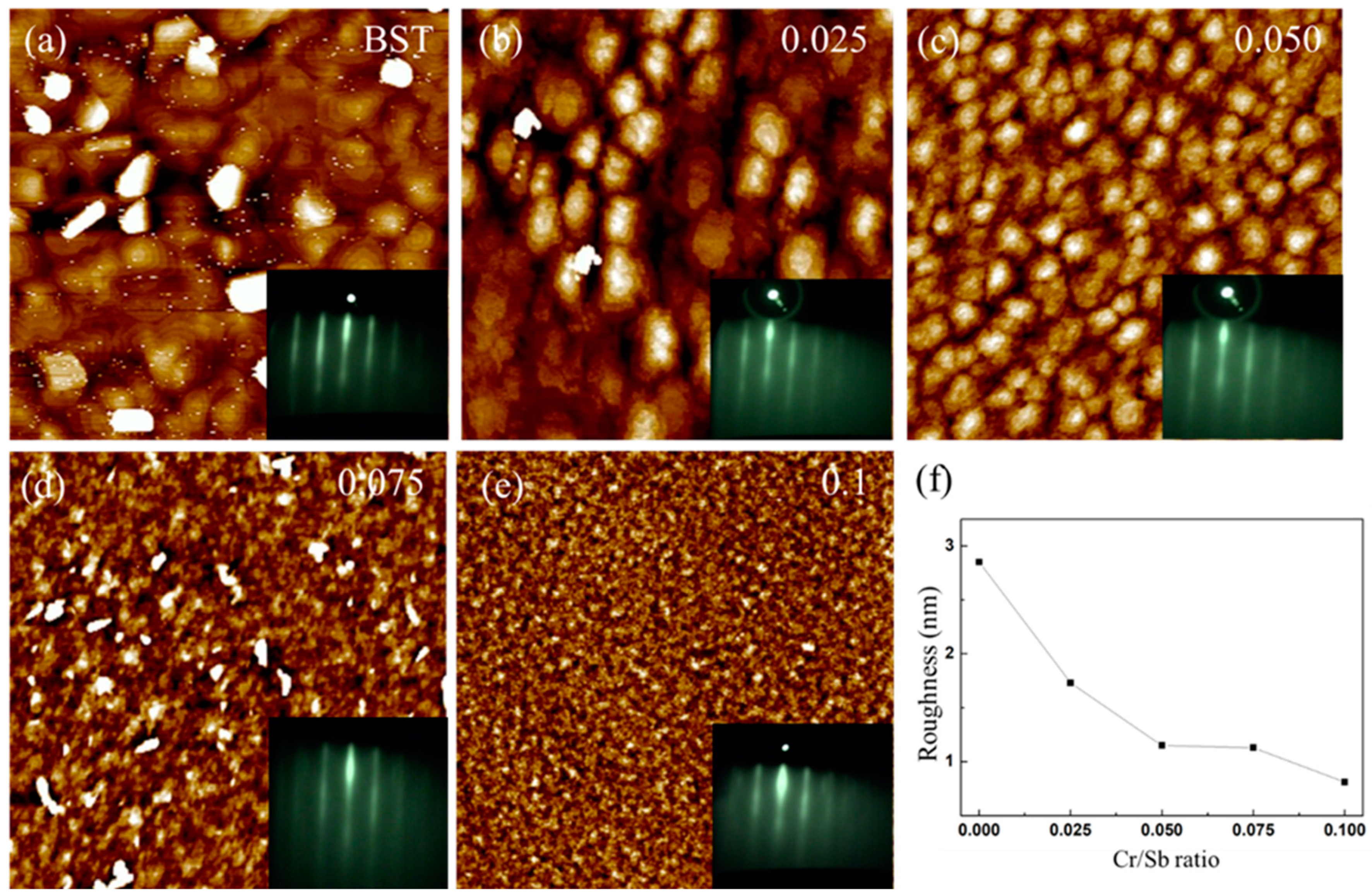
3.1. Cr-Doped (Bi0.4Sb0.6)2Te3 with the Cr/Sb Flux Ratio and Growth Temperature

XRD analysis was conducted to investigate the influence of temperature and Cr doping concentrations on the structure of Cr:BST films. First, we studied the growth temperature effect under a fixed Cr/Sb ratio of 0.1. A growth temperature of 200 °C is insufficient to promote the epitaxial growth of Cr:BST, as illustrated by the XRD in Figure 1a. For a temperature of 300 °C, the appearance of the diffraction lattice planes at (003), (006), (009), (0012), (0015), (0018), (0021), and (0024) confirms the ordered rhombohedral structure of the films, consistent with previous studies [22,25]. The ordered rhombohedral structure is slightly weakened as the growth temperature increases to 400 °C. When the growth temperature is further raised to 500 °C, the (00l) peaks disappear, and (112) and (224) peaks of Cr2Te3 emerge [30,31]. This indicates that the elevated temperature is sufficient to significantly reduce the condensation of Bi and Sb elements on the substrate, facilitating the formation of Cr2Te3. At the optimal growth temperature of 300 °C, the impact of Cr doping concentration on the structure of Cr:BST was studied in Figure 1b. The XRD spectra display prominent characteristic (00l) signals, with all the peaks normalized to the (0015) peaks for comparison. When the Cr/Sb ratio is in the range from 0 to 0.1, the structure of Cr:BST films reflects the ordered rhombohedral structure. Notably, the (0015), (0018), and (0021) peaks exhibit a slight shift to higher angles with an increasing Cr/Sb ratio. This phenomenon aligns with the Sherrer equation, where the shift of the XRD peaks is in proportion to the relation with the lattice parameter of the material. Therefore, the shift of the XRD peaks can be attributed to the incorporation of Cr, wherein the substitution of Bi/Sb by Cr leads to a reduction in the crystal lattice parameter. This reduction arises from the smaller ionic radius of Cr compared to Sb and Bi [32,33], as confirmed by the reduction in the c-axis lattice parameters of (0015) from 30.53 ± 0.05 to 30.06 ± 0.04 Å with an elevated Cr/Sb ratio, as shown in Figure 1c [34,35]. Additionally, the intensity of the signal peak (003) strengthens with the increase in Cr concentration, likely corresponding to an enhancement of surface smoothness. However, when the samples are doped with a Cr/Sb ratio above 0.2, Cr2Te3 signals appear, and the characteristic (00l) peaks of BST vanish (Figure S1a).
Figure 1d shows the HRTEM image along the c-axis direction, clearly revealing the characteristic quintuple-layer (QL) structure with van der Waals (vdW) stacking in a Cr:BST epitaxial film. The film thickness was identified as 25 QL. The effect of the various Cr doping concentrations on lattice vibration of the Cr:BST was qualitatively studied using Raman spectroscopy with an excitation wavelength of 532 nm at a frequency range of 100–200 cm−1. In Figure 1e, the BST sample exhibits three primary Raman active modes at 126.7, 141.2, and 163.5 cm−1, corresponding to three modes, E g 2 , A1u, and A 1 g 2 , respectively [36,37]. The A1u and A 1 g 2 modes are sensitive to the out-of-plane Bi/Sb-Te bond vibrations, while E g 2 mode is sensitive to the in-plane Bi/Sb-Te bond vibration [36,38,39]. Moreover, E g 2 modes involve in-plane bending, where the bonding of each atom is stronger (covalent bonds) than out-of-plane (vdW forces) [39]. It is noted that E g 2 mode slightly shifts toward higher wavenumbers as the Cr/Sb ratio increases [36], while A1u mode remains constant (Figure S2).
The observed blueshift in E g 2 modes could be attributed to structural distortion due to the substitution of Sb or Bi by Cr atoms [40]. First-principle calculations further support this by indicating that the formation energies of Cr favor the substitution of Bi sites in BST [19]. As the Cr/Sb ratio increased, the intensity of the three modes was notably attenuated, indicating a deterioration in the bulk structural quality with an elevated Cr concentration. Additionally, to gain insights into the chemical environment of Cr within the sample, we conducted XPS measurements, focusing on the Cr core level. Unfortunately, the XPS peaks of Cr 2p3/2 and 2p1/2 orbital overlaps with the Te 3d5/2 and 3d1/2 orbitals, and the peak of the Cr 3p orbital overlaps with the Te 4d3/2 and 4d5/2 orbitals. Aside from that, the XPS signal intensities of the Cr 2s and 3s orbitals and the Te 3p1/2 and 3p3/2 orbitals are very weak. Therefore, we chose the peaks of Cr 2p and the Te 3d orbitals, which show the strongest XPS signal that can be used to confirm the chemical bond states of Cr. Figure 1f shows the deconvolution of the Te 3d core levels for the Cr/Sb = 0.1 sample. The binding energy of Te 3d5/2 and 3d1/2 core levels (blue peaks) are determined to be 572.60 eV and 582.5 eV, respectively. The Te percentage is much larger than Cr, resulting in a weaker Cr signal intensity. The discernment of the Cr signal necessitates deconvolution peaks using a multi-peak Lorentz fitting with the uncertainty shown in Figure S3. From the fitting results, the binding energy of Cr 2p3/2 and 2p1/2 core levels (green peaks) are located at 573.1 eV and 583.5 eV, respectively. Therefore, the XPS result confirms the valence states of Cr in Cr:BST samples.
The surface morphology of Cr-doped (Bi0.4Sb0.6)2Te3, grown at 300 °C with varying Cr/Sb ratios from 0 to 0.1, was quantitatively examined by AFM measurements. Figure 2a shows the AFM image of the grown BST film, indicating a reasonably flat surface characterized by distinct terraces and steps, reflecting the hexagonal crystal structure of BST grown along (0001), which is consistent with the aforementioned XRD results. With the increasing Cr/Sb ratio, the surface morphology reveals misoriented domains with ambiguous shapes, as shown in Figure 2b–e. We have also examined the surface morphology of Cr:BST grown with Cr/Sb ratios of 0.2 and 0.3, as shown in Figure S1b,c. Additionally, the RHEED patterns consistently show sharp 1 × 1 diffraction streaks across various Cr/Sb ratios, indicating high crystalline order and relatively smooth surface morphologies (insets of Figure 2a–e). The surface roughness of Cr:BST films decreased from 2.8 to 0.4 nm as the Cr/Sb ratio increased from 0 to 0.1. These structural features, confirmed by AFM, HRTEM, and XRD, reveal the high quality of the Cr:BST films grown by the delicate MBE method.

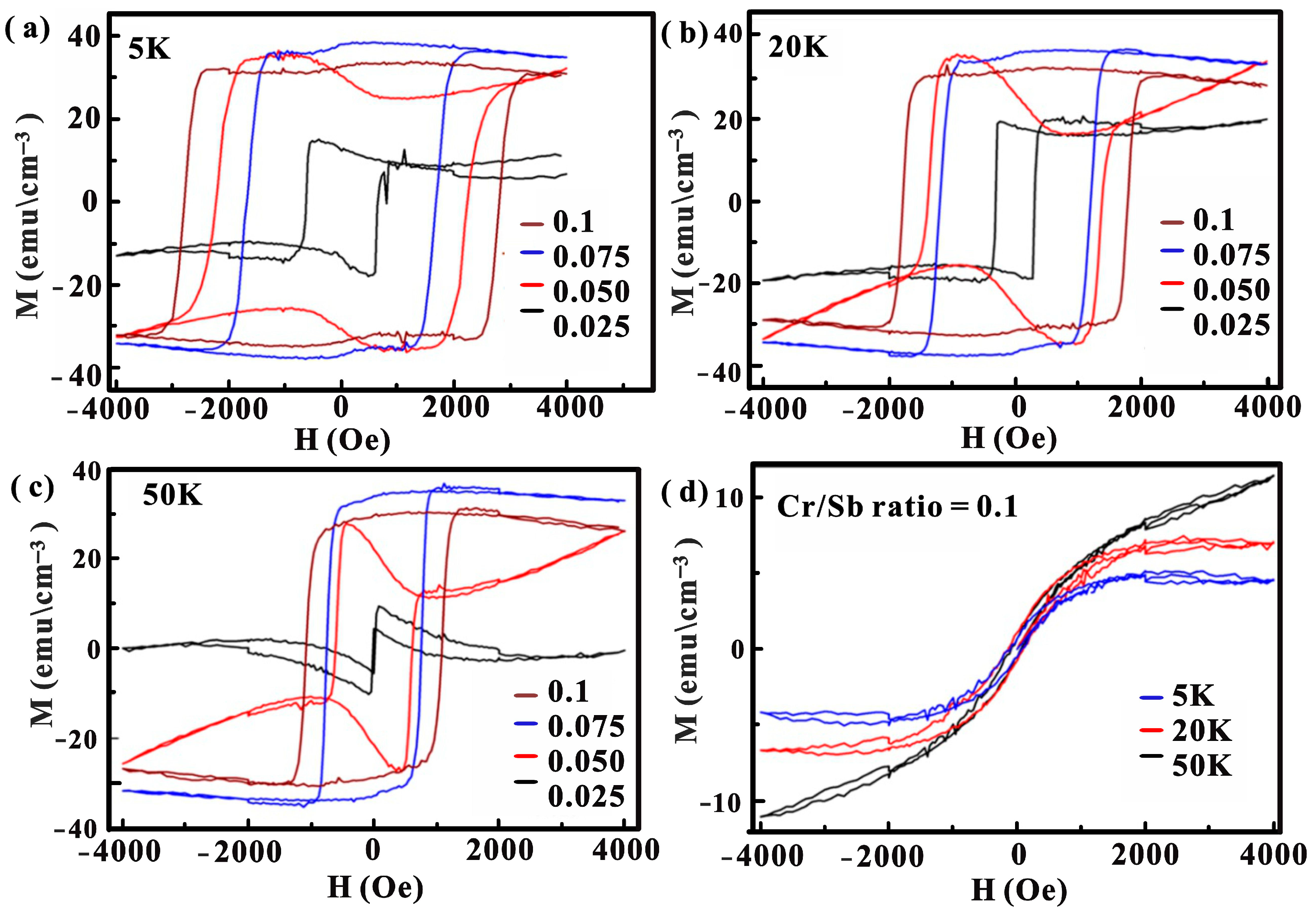
3.2. Magnetic Properties

A SQUID magnetometer was employed to investigate the magnetic properties of Cr-doped (Bi0.4Sb0.6)2Te3 films with varying Cr/Sb ratios from 0 to 0.1. The diamagnetic signal due to the substrate was subtracted by fitting to the high-field data and subsequently removing the diamagnetic background (Figure S4).
Figure 3a–c present the magnetization curves of Cr-doped (Bi0.4Sb0.6)2Te3 samples with different Cr/Sb ratios obtained at temperatures of 5, 20, and 50 K, with the magnetic field applied along the out-of-plane direction (H//c) of the samples. The out-of-plane M-H hysteresis loops reveal ferromagnetic behavior along the easy axis. Note that the out-of-plane saturation magnetization and coercivity increase with an increasing Cr/Sb ratio (Table 1 and Table 2). Evidently, the Tc of the Cr:BST sample with a Cr/Sb ratio of ~0.025 falls below 50 K. In contrast, the Cr:BST samples with a higher Cr/Sb ratio over 0.05 exhibit Tc above 50 K. Additionally, the M-H curve for the 0.05 sample shows non-square loop behavior, which might be attributed to the substrate effect [28].
The magnetic effect of the Cr doping in BST films can be elucidated through two primary mechanisms: the van Vleck mechanism and Ruderman–Kittel–Kasuya–Yosida (RKKY) coupling [19,41,42]. In the case of the van Vleck mechanism, the significant spin susceptibility of valence electrons in band-inverted TIs materials enables direct coupling of magnetic ions through these localized valence electrons, bypassing the need for itinerant electrons. This leads to what is termed “bulk ferromagnetism”, which is not dependent on carrier density [1]. On the other hand, the RKKY interaction involves coupling between neighboring magnetic ions via the mediation of conduction carriers, known as carrier-mediated RKKY interaction [41,42]. Moreover, the RKKY mechanism is particularly evident in bulk p-type Cr-doped BST samples [43,44]. In this case, the Tc is found to be proportional to n p 1/3, where n p is the hole carrier density. The ferromagnetism in this scenario is strongly related to the hybridization between the transition-metal d states and the anion p states [44]. Notably, higher Cr doping concentrations lead to elevated Tc values because of the shorter distances among the Cr atoms and the more robust interactions between them. The magnetization curves of Cr-doped (Bi0.4Sb0.6)2Te3 film (Cr/Sb ratio~0.1) with a magnetic field along the in-plane direction at 5, 20, and 50 K were illustrated in Figure 3d. The in-plane M-H loops flat curves, resembling a hard-axis configuration. The results suggested the Cr:BST films unveiled a perpendicular magnetic anisotropy with the easy magnetization axis along the c-axis, holding significance for the development of ferromagnetic topological insulators in the context of QAH studies and spintronic applications.

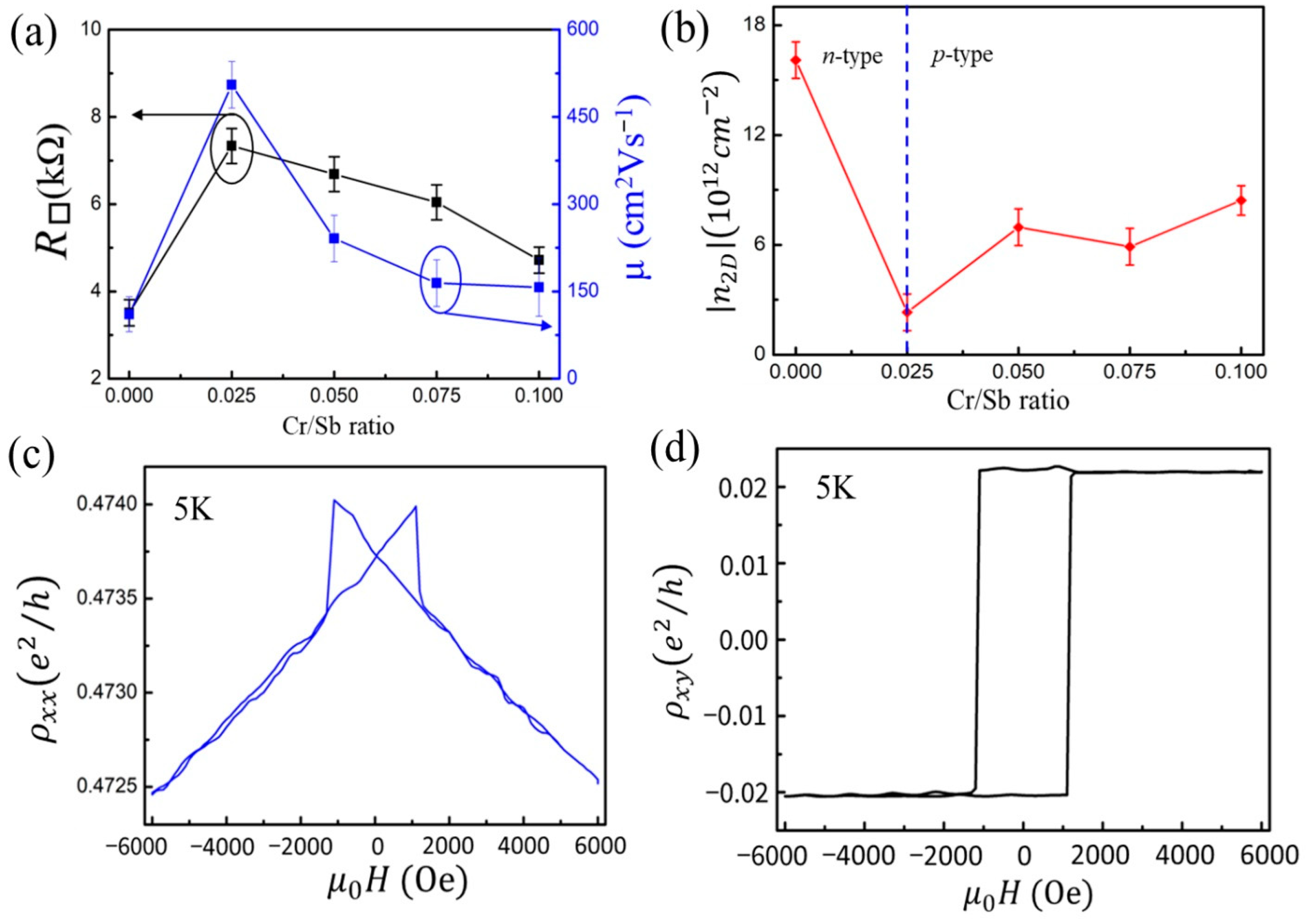
3.3. Transport Properties

The influence of various Cr/Sb ratios is also evident in the transport properties. The electrical properties of Cr:BST samples were studied by analyzing the longitudinal resistance Rxx and Hall resistance Rxy at temperatures of 16 K with a magnetic field up to 20,000 Oe. Figure 4a summarizes the evolution of sheet resistance (R) and carrier mobility with various Cr/Sb ratios. The R of the Cr:BST sample shows a maximum at a Cr/Sb ratio of 0.025, subsequently decreasing as the Cr/Sb ratio further increases to 0.1, as depicted on the left side in Figure 4a. Additionally, the carrier mobility of Cr:BST also increases until a Cr/Sb ratio of 0.025 reaches its maximum and then decreases as the Cr/Sb ratio further rises to 0.1, as shown on the right side in Figure 4a. Notably, the carrier mobility of Cr:BST with a Cr/Sb ratio of 0.025 is about five times larger than the BST sample. Figure 4b displays the carrier concentration of Cr:BST samples as a function of the Cr/Sb ratio. In the absence of Cr doping, the (Bi0.4Sb0.6)2Te3 sample exhibits n-type conductivity, which is consistent with previous results reported for (BixSb1−x)2Te3 [2]. The carrier density |n2D| of Cr:BST films reaches its minimum at a Cr/Sb ratio of 0.025 with |n2D|= 2.3 × 1012 cm−2 and increases on both sides. The incorporation of Cr adjusts the charge carrier in Cr:BST samples, transitioning from n-type to p-type, and the hole concentration slightly increases with higher Cr doping levels. The results suggest that the BST composition (Bi0.4Sb0.6)2Te3 is close to the desired value, allowing the Cr dopant to modulate the charge carrier type with a low bulk carrier concentration and high carrier mobility, inducing ferromagnetism in BST topological insulators. The ferromagnetic ordering in Cr:BST films was further confirmed by magneto-transport measurements. For clarity, we focus on the sample with a Cr/Sb ratio of 0.025, showing low bulk carrier concentration and high carrier mobility. Figure 4c,d display the Hall resistivity ( ρ x y ) and longitudinal resistivity ( ρ x x ) measured at 5 K in a magnetic field up to 6000 Oe applied perpendicular to the films. The ρ x x shown in Figure 4c exhibits a butterfly-shaped curve and two double-split sharp peaks located at the coercive field HC that decreased rapidly on both sides, which is consistent with previous results for Cr-doped BST films [22].
Figure 4d displays clear hysteresis loops of anomalous Hall resistivity, implying the well-defined perpendicular ferromagnetism in the Cr:BST. However, the ρ x y only reaches 0.02 (e2/h), indicating that it is not ideal yet for achieving the QAHE. While the full quantization of the QAHE signal remains unachieved, we anticipate that further refinement of the composition of (BixSb1−x)2Te3 and Cr doping levels, along with the application gate voltage on the Hall effect device, will unveil and optimize the QAHE in this system.

4. Conclusions

In summary, we have presented a synthesis and characterizations of Cr-doped (Bi0.4Sb0.6)2Te3 (Cr:BST) films prepared using MBE. By carefully controlling the epitaxy growth conditions, we have demonstrated the preparation of high-quality, single-crystalline Cr:BST samples, as confirmed by XRD. The AFM and HRTEM analyses further confirmed a flat surface morphology covering a large area, with evidence of van der Waals stacking. Raman spectroscopy provided insight into the impact of Cr doping on the structure, indicating a discernible blue shift in signals due to the substitution of Sb or Bi by Cr. The existence of Cr states in Cr:BST samples was unequivocally confirmed through XPS results. The magnetic behavior of Cr:BST films exhibited perpendicular magnetic anisotropy with Tc above 50 K. Further, the evolution of sheet resistance and carrier mobility reached peak maximum for the Cr:BST sample with a Cr/Sb ratio of 0.025, aligning with the electronic behavior displaying a transition from n-type to p-type carriers. Hall and longitudinal resistance measurements confirmed that the Cr: BST sample with a Cr/Sb ratio of 0.025 exhibited an AHE effect at 5 K. These findings collectively underscore the intricate interplay between Cr doping levels and the resulting structural, magnetic, and electronic properties of Cr-doped (Bi0.4Sb0.6)2Te3 films. Although the complete quantization of the quantum anomalous Hall effect signal has not yet been accomplished, we foresee that through additional fine-tuning of the composition of (BixSb1−x)2Te3 and the levels of Cr doping, coupled with the application of gate voltage on the Hall effect device, we can reveal and optimize the QAHE in this system. This study provides valuable insights for applications in emerging technologies, such as the quantum anomalous Hall effect and spintronic applications, based on magnetic topological insulators.

Supplementary Materials

The following supporting information can be downloaded at https://www.mdpi.com/article/10.3390/nano14020157/s1, Figure S1. XRD and AFM results of Cr:BST with Cr/Sb ratio of 0.1–0.3; Figure S2. Three Raman active modes as a function of Cr/Sb ratio. Figure S3. The Te 3d core level for Cr:BST sample with Cr/Sb = 0.1 and BST sample. Figure S4. The original SQUID data of Cr/Sb = 0.025 sample at 20 K. Refs. [33,45,46] are cited in the supplementary materials.

Author Contributions

C.-C.H. undertook the MBE growth of the samples and the XRD, SQUID, TEM, and Raman experiments. M.K.L. assisting with the PPMS and SQUID experiments. P.G., S.H.S. and J.-C.-A.H. wrote and revised the manuscript with input from all authors. All authors discussed the results. All authors have read and agreed to the published version of the manuscript.

Funding

We would like to acknowledge financial support from the Taiwan Ministry of Science and Technology, which supported this research financially under contracts NSTC 110-2124-M-006-008 and 109-2112-M-006-019-MY3.

Data Availability Statement

All data included in this study are available upon request by contacting the corresponding author.

Acknowledgments

The authors gratefully acknowledge the use of XRD 003100, SQUID 000200, and EM 012300 belonging to the Core Facility Center of National Cheng Kung University.

Conflicts of Interest

The authors declare no conflicts of interest.

References

  1. Rui, Y.; Wei, Z.; Hai, J.Z.; Shou, C.Z.; Xi, D.; Zhong, F. Quantized anomalous Hall effects in magnetic topological insulator. Science 2010, 329, 61–64. [Google Scholar]
  2. Zhang, J.; Chang, C.Z.; Zhang, Z.; Jing, W.; Xiao, F.; Kang, L.; Minhao, L.; Ke, H.; Lili, W.; Xi, C.; et al. Band structure engineering in (Bi1−xSbx)2Te3 ternary topological insulators. Nat. Commun. 2011, 2, 574. [Google Scholar] [CrossRef] [PubMed]
  3. Goldsmid, H.J. Recent Studies of Bismuth Telluride and Its Alloys. J. Appl. Phys. 1961, 32, 2198–2202. [Google Scholar] [CrossRef]
  4. Hamawandi, B.; Ballikaya, S.; Batili, H.; Roosmark, V.; Orlovská, M.; Yusuf, A.; Johnsson, M.; Szukiewicz, R.; Kuchowicz, M.; Toprak, M.S. Facile Solution Synthesis, Processing and Characterization of n- and p-Type Binary and Ternary Bi–Sb Tellurides. Appl. Sci. 2020, 10, 1178. [Google Scholar] [CrossRef]
  5. Xu, Z.J.; Hu, L.P.; Ying, P.J.; Zhao, X.B.; Zhu, T.J. Enhanced thermoelectric and mechanical properties of zone melted p-type (Bi,Sb)2Te3 thermoelectric materials by hot deformation. Acta Mater. 2015, 84, 1359–6454. [Google Scholar] [CrossRef]
  6. Hohler, H.; Freudenberger, A. Investigation of the highest valance band in (Bi1−xSbx)2Te3. Phys. Stat. Sol. 1977, 84, 195. [Google Scholar]
  7. He, X.; Li, H.; Chen, L.; Wu, K. Substitution-induced spin-splitted surface states in topological insulator (Bi1−xSbx)2Te3. Sci. Rep. 2015, 5, 8830. [Google Scholar] [CrossRef]
  8. Ryota, A.; Kazuki, S.; Satoru, I.; Ryosuke, N.; Akio, K.; Konstantin, A.K.; Oleg, E.T.; Shuji, H. Shubnikov-de Hass oscillations in p and n-type topological insulator (BixSb1−x)2Te3. J. Phys Condens. Matter 2018, 30, 265001. [Google Scholar]
  9. Chang, C.Z.; Zhang, J.; Feng, X.; Shen, J.; Zhang, Z.; Guo, M.; Li, K.; Ou, Y.; Wei, P.; Wang, L.-L.; et al. Experimental observation of the quantum anomalous Hall effect in a magnetic topological insulator. Science 2013, 340, 167. [Google Scholar] [CrossRef]
  10. Qi, X.L.; Wu, Y.S.; Zhang, S.C. Topological quantization of the spin Hall effect in two-dimensional paramagnetic semiconductors. Phys. Rev. B 2006, 8, 085308. [Google Scholar] [CrossRef]
  11. Checkelsky, J.; Ye, J.; Onose, Y.; Tokura, Y. Dirac-fermion-mediated ferromagnetism in a topological insulator. Nat. Phys. 2012, 8, 729–733. [Google Scholar] [CrossRef]
  12. Qi, X.L.; Zhang, S.C. Topological insulator and superconductors. Rev. Mod. Phys. 2011, 83, 1057. [Google Scholar] [CrossRef]
  13. Zhenhua, Z.; Ctirad, U.; Zabcik, M.; Lostak, P. Carrier-mediated ferromagnetism in vanadium-doped (Sb1−xBix)2Te3 solid solutions. Appl. Phys. Lett. 2006, 88, 192502. [Google Scholar] [CrossRef]
  14. Liu, M.H.; Zhang, J.S.; Chang, C.Z.; Zhang, Z.C.; Feng, X.; Li, K.; He, K.; Wang, L.L.; Chen, X.; Dai, X.; et al. Crossover between Weak Antilocalization and Weak Localization in a Magnetically Doped Topological Insulator. Phys. Rev. Lett. 2012, 108, 036805. [Google Scholar] [CrossRef] [PubMed]
  15. Xu, S.Y.; Neupane, M.; Liu, C.; Zhang, D.M.; Richardella, A.; Wray, L.; Alidoust, N.; Leandersson, M.; Balasubramanian, T.; Barriga, J.; et al. Hedgehog Spin Texture and Berry’s Phase Tuning in a Magnetic Topological Insulator. Nat. Phys. 2012, 8, 616–622. [Google Scholar] [CrossRef]
  16. Chen, Y.L.; Chu, J.H.; Analytis, J.G.; Liu, Z.K.; Igarashi, K.; Kuo, H.H.; Qi, X.L.; Mo, S.K.; Moore, R.G.; Lu, D.H.; et al. Massive Dirac Fermion on the surface of a magnetically doped topological insulator. Science 2010, 329, 659–662. [Google Scholar] [CrossRef]
  17. Qi, X.L.; Taylor, L.; Shou, C.Z. Topological field theory of time-reversal invariant insulator. Phys. Rev. B 2008, 48, 195424. [Google Scholar] [CrossRef]
  18. Cui, Z.C.; Jinsong, Z.; Minhao, L.; Zuocheng, Z.; Xiao, F.; Kang, L.; Li, L.W.; Xi, C.; Xi, D.; Zhong, F.; et al. Thin Films of Magnetically Doped Topological Insulator with Carrier-Independent Long-Range Ferromagnetic Order. Adv. Mater. 2013, 25, 1065–1070. [Google Scholar]
  19. Kou, X.F.; Shih, T.G.; Yabin, F.; Lei, P.; Murong, L.; Ying, J.; Qiming, S.; Tianxiao, N.; Koichi, M.; Jianshi, T.; et al. Scale-invariant quantum anomalous Hall effect in magnetic topological insulators beyond the two-dimensional limit. Phys. Rev. Lett. 2014, 113, 137201. [Google Scholar] [CrossRef]
  20. Xufeng, K.; Lei, P.; Jing, W.; Yabin, F.; Eun, S.C.; Wei, L.L.; Tianxiao, N.; Koichi, M.; Qiming, S.; Shou, C.Z.; et al. Meta-to-insulator switching in quantum anomalous Hall states. Nat. Commun. 2015, 6, 8474. [Google Scholar]
  21. Mogi, M.; Kawamura, M.; Yoshimi, R.; Tsukazaki, A.; Kozuka, Y.; Shirakawa, N.; Takahashi, K.S.; Kawasaki, M.; Tokura, Y. A magnetic heterostructure of topological insulators as a candidate for an axion insulator. Nat. Mater. 2017, 16, 516–521. [Google Scholar] [CrossRef] [PubMed]
  22. Xufeng, K.; Murong, L.; Yabin, F.; Ying, J.; Tianxiao, N.; Jianmin, Z.; Wanjun, J.; Yong, W.; Yugui, Y.; Liang, H.; et al. Interplay between Different Magnetisms in Cr-Doped Topological Insulators. ACS Nano 2013, 7, 9205–9212. [Google Scholar]
  23. Adam, A.M.; Petkov, P. Structural and optical properties of nano-powder-based (Sb1−xBix)2Te3 thin films. Mater. Res. Express 2017, 4, 08502. [Google Scholar] [CrossRef]
  24. Kašparová, J.; Drašar, Č.; Krejčová, A.; Beneš, L.; Lošt’ák, P.; Chen, W.; Zhou, Z.; Uher, C. n-type to p-type crossover in quaternary BixSbyPbzSe3 single crystals. J. Appl. Phys. 2005, 97, 103720. [Google Scholar] [CrossRef]
  25. Yan, N.; Zhen, Z.; Nlebedim, C.I.; Jiles, D.C. Magnetotransport study of (Sb1−xBix)2Te3 thin films on mica substrate for ideal topological insulator. AIP Adv. 2016, 6, 055812. [Google Scholar]
  26. Liu, Y.; Li, Y.; Rajput, S.; Gilks, D.; Lari, L.; Galindo, P.L.; Weinert, M.; Lazarov, V.K.; Li, L. Tuning Dirac states by strain in the topological insulator Bi2Se3. Nat. Phys. 2014, 10, 294–299. [Google Scholar] [CrossRef]
  27. Su, S.-H.; Chang, J.-T.; Chuang, P.-Y.; Tsai, M.-C.; Peng, Y.-W.; Lee, M.K.; Cheng, C.-M.; Huang, J.-C.A. Epitaxial Growth and Structural Characterizations of MnBi2Te4 Thin Films in Nanoscale. Nanomaterials 2021, 11, 3322. [Google Scholar] [CrossRef]
  28. Su, S.-H.; Chuang, P.-Y.; Lee, J.-C.; Chong, C.-W.; Li, Y.W.; Lin, Z.M.; Chen, Y.-C.; Cheng, C.-M.; Huang, J.-C.A. Spin-to-Charge Conversion Manipulated by Fine-Tuning the Fermi Level of Topological Insulator (Bi1–xSbx)2Te3. ACS Appl. Electron. Mater. 2021, 3, 2988–2994. [Google Scholar] [CrossRef]
  29. Gultom, P.; Chiang, J.-Y.; Huang, T.-T.; Lee, J.-C.; Su, S.-H.; Huang, J.-C.A. Structural and Optical Properties of Tungsten Disulfide Nanoscale Films Grown by Sulfurization from W and WO3. Nanomaterials 2023, 13, 1276. [Google Scholar] [CrossRef]
  30. Ramasamy, K.; Mazumdar, D.; Bennett, R.D.; Gupta, A. Syntheses and magnetic properties of Cr2Te3 and CuCr2Te4 nanocrystals. Chem. Commun. 2012, 48, 5656–5658. [Google Scholar] [CrossRef]
  31. Burn, D.M.; Duffy, L.B.; Fujita, R.; Zhang, S.L.; Figueroa, A.I.; Herrero-Martin, J.; van der Laan, G.; Hesjedal, T. Cr2Te3 Thin Films for Integration in Magnetic Topological Insulator Heterostructures. Sci. Rep. 2019, 9, 10793. [Google Scholar] [CrossRef]
  32. Adam, A.M.; Lilov, E.; Lilova, V.; Petkov, P. Characterization and optical properties of bismuth chalcogenide films prepared by pulsed laser deposition technique. Mater. Sci. Semicond. Process. 2017, 57, 1369–8001. [Google Scholar] [CrossRef]
  33. Ho, Y.; Sekwon, N.; Jun, G.G.; Seong, J.J.; Seungmin, H.; Hoo, J.L. Effects of Sb content (x) on (Bi1−xSbx)2Te3 thermoelectric thin film deposited by Effusion cell evaporator. J. Nanosci. Nanotechno 2015, 15, 10. [Google Scholar]
  34. Bessas, D.; Sergueev, I.; Wille, H.C.; Persson, J.; Ebling, D.; Hermann, R.P. Lattice dynamics in Bi2Te3 and Sb2Te3: Te and Sb density of phonon states. Phys. Rev. B 2012, 86, 224301. [Google Scholar] [CrossRef]
  35. Liu, Z.; Xinyuan, W.; Jiajia, W.; Hong, P.; Fuhao, J.; Mao, Y.; Zhongqian, Y.; Shan, Q. Local atomic and electronic structures in ferromagnetic topological insulator Cr-doped (BixSb1−x)2Te3 studied by XAFS and ab initio calculations. Phys. Rev. B 2015, 92, 10. [Google Scholar]
  36. Rajashri, R.U.; Umesh, A.P. Phonon dynamics of (Bi1−xSbx)2Te3 topological insulator by Raman spectroscopy. Phys. B Condens. Matter 2023, 655, 0921–4526. [Google Scholar]
  37. Richter, W.; Becker, C.R. A Raman and far-infrared investigation of phonons in the rhombohedral V2-VI3 compounds Bi2Te3, Bi2Se3, Sb2Te3 and Bi2(Te1−xSex)3 (0 < x < 1), (Bi1−ySby)2Te3 (0 < y < 1). Phys. Stat. Sol. 1977, 84, 619. [Google Scholar]
  38. Weyrich, C.; Drögeler, M.; Kampmeier, J.; Eschbach, M.; Mussler, G.; Merzenich, T.; Stoica, T.; Batov, I.E.; Schubert, J.; Plucinski, L.; et al. Growth, characterization, and transport properties of ternary (Bi1−xSbx)2Te3 topological insulator layers. J. Phys. Condens. Matter 2016, 28, 495501. [Google Scholar] [CrossRef]
  39. Shahil, K.M.F.; Hossain, M.Z.; Goyal, V.; Balandin, A.A. Micro-Raman spectroscopy of mechanically exfoliated few-quintuple layers of Bi2Te3, Bi2Se3, and Sb2Te3 materials. J. Appl. Phys. 2012, 111, 054305. [Google Scholar] [CrossRef]
  40. Zhang, C.; Zeping, P.; Zhong, L.; Ligen, Y.; Khia, A.K.; Qihuan, X. Controlled growth of bismuth antimony telluride BixSb2xTe3 nanoplatelets and their bulk thermoelectric nanocomposites. Nano Energy 2015, 15, 2211–2855. [Google Scholar] [CrossRef]
  41. Ruderman, M.A.; Kittel, C. Indirect Exchange Coupling of Nuclear Magnetic Moments by Conduction Electrons. Phys. Rev. 1954, 96, 99–102. [Google Scholar] [CrossRef]
  42. Jungwirth, T.; Sinova, J.; Masek, J.; Kucera, J.; MacDonald, A.H. Theory of Ferromagnetic (III, Mn)V Semiconductors. Rev. Mod. Phys. 2006, 78, 809–864. [Google Scholar] [CrossRef]
  43. Li, B.; Fan, Q.; Ji, F.; Liu, Z.; Pan, H.; Qiao, S. Carrier dependent ferromagnetism in chromium doped topological insulator, Cry(BixSb1−x)2−yTe3. Phys. Lett. A 2013, 377, 1925. [Google Scholar] [CrossRef]
  44. Fan, Q.; Li, B.; Ji, F.; Liu, Z.; Pan, H.; An, Z.; Qiao, S. Resistivity and p–d Exchange Interaction in Cr0.2Sb(1.8−x)BixTe3. Appl. Phys. Exp. 2013, 6, 053003. [Google Scholar] [CrossRef]
  45. Huang, H.; Shen, J.; Chen, J.; Shen, Q.; Lin, G.; Zhu, Z.; Wu, J.; Ma, J.; Yang, H.; Liu, X.; et al. Controllable phase transition of two-dimensional ferromagnetic chromium telluride thin films grown by molecular beam epitaxy. Quantum Front. 2023, 2, 12. [Google Scholar] [CrossRef]
  46. Yu, F.; Yin, Y.; Liu, G.; Tian, Q.; Meng, Q.; Zhao, W.; Wang, K.; Wang, C.; Yang, S.; Wu, D.; et al. Thickness-dependent structural phase transition and self-intercalation of two-dimensional ferromagnetic chromium telluride thin films. Appl. Phys. Lett. 2022, 120, 261602. [Google Scholar] [CrossRef]
Figure 1. XRD diagrams for (a) a fixed Cr/Sb ratio of 0.1 under varied growth temperatures (indicated on the right-hand axis) and (b) a fixed growth temperature at 300 °C with varied Cr/Sb ratios (indicated on the right-hand axis). The signals are marked as asterisks for the c-plane Al2O3 substrate indicated in the figure. (c) c-axis lattice parameter extracted from (0015) peak as a function of the Cr/Sb ratio. (d) TEM cross-sectional view of the film with a Cr/Sb ratio of 0.1 and a growth temperature of 300 °C. (e) Raman spectra of films with varied Cr/Sb ratios, with dashed vertical lines highlighting the three Raman active modes, E g 2 , A1u, and A 1 g 2 . (f) XPS spectra of Cr 2p and Te 3d orbitals of the Cr/Sb ratio of the 0.1 sample. The black dots are the XPS spectra, and the blue and green curves are the Lorentz fitting curves corresponding to the Cr 2p and Te 3d orbitals, while the red curves are the total fitting curves. Note: * sign: c-plane Al2O3 substrate signals.
Nanomaterials 14 00157 g001
Figure 2. (ae) Dependence of film morphology on Cr:BST samples with varied Cr/Sb ratios from an AFM (all images have a scan size of 2 μm × 2 μm). Inset corresponds to RHEED patterns. (f) Roughness for varied Cr/Sb ratios.
Nanomaterials 14 00157 g002
Figure 3. (ac) Hysteresis loops of the Cr:BST samples with various Cr/Sb ratios in a magnetic field along an out-of-plane direction at different temperatures of 5, 20, and 50 K, respectively. (d) Hysteresis loops of a Cr/Sb ratio of a 0.1 sample in a magnetic field along the in-plane direction at different temperatures.
Nanomaterials 14 00157 g003
Figure 4. (a) The sheet resistance (R) (left ordinate axis) and mobility (left ordinate axis) of Cr:BST samples with varied Cr/Sb ratios. (b) The absolute value of the sheet electron concentration n2D of Cr:BST with varied Cr/Sb ratios. (c) Magnetic field-dependent longitudinal resistance curves at 5 K of the Cr:BST sample with a Cr/Sb ratio of 0.025. (d) A rectangular-shaped hysteresis loop in magnetic field-dependent Hall resistance curves at 5 K of the Cr:BST sample with a Cr/Sb ratio = 0.025.
Nanomaterials 14 00157 g004
Table 1. The temperature-dependent saturation magnetization of Cr-doped (Bi0.4Sb0.6)2Te3 at different Cr/Sb ratios.
Temperatures
(K)
Cr/Sb Ratio
0.0250.050.0750.1
517.536.638.533.9
2018.736.037.732.5
50-27.934.730.9
Notes: (unit of saturation magnetization: emu/cm−3).
Table 2. The temperature-dependent coercivity of Cr-doped (Bi0.4Sb0.6)2Te3 with different Cr/Sb ratios.
Temperatures
(K)
Cr/Sb Ratio
0.0250.050.0750.1
5630223016802800
20300137011901780
50-6107501080
Notes: (unit of coercivity: Oe).
Disclaimer/Publisher’s Note: The statements, opinions and data contained in all publications are solely those of the individual author(s) and contributor(s) and not of MDPI and/or the editor(s). MDPI and/or the editor(s) disclaim responsibility for any injury to people or property resulting from any ideas, methods, instructions or products referred to in the content.

