
Thermoelectric Sensor with CuI Supported on Rough Glass


Abstract
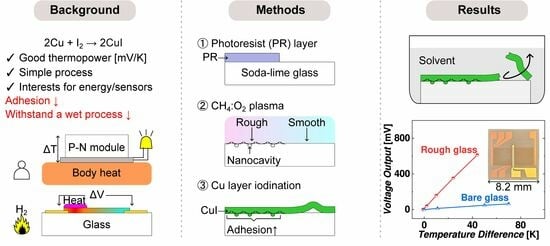
1. Introduction
2. Materials and Methods
2.1. Device
2.2. Fabrication
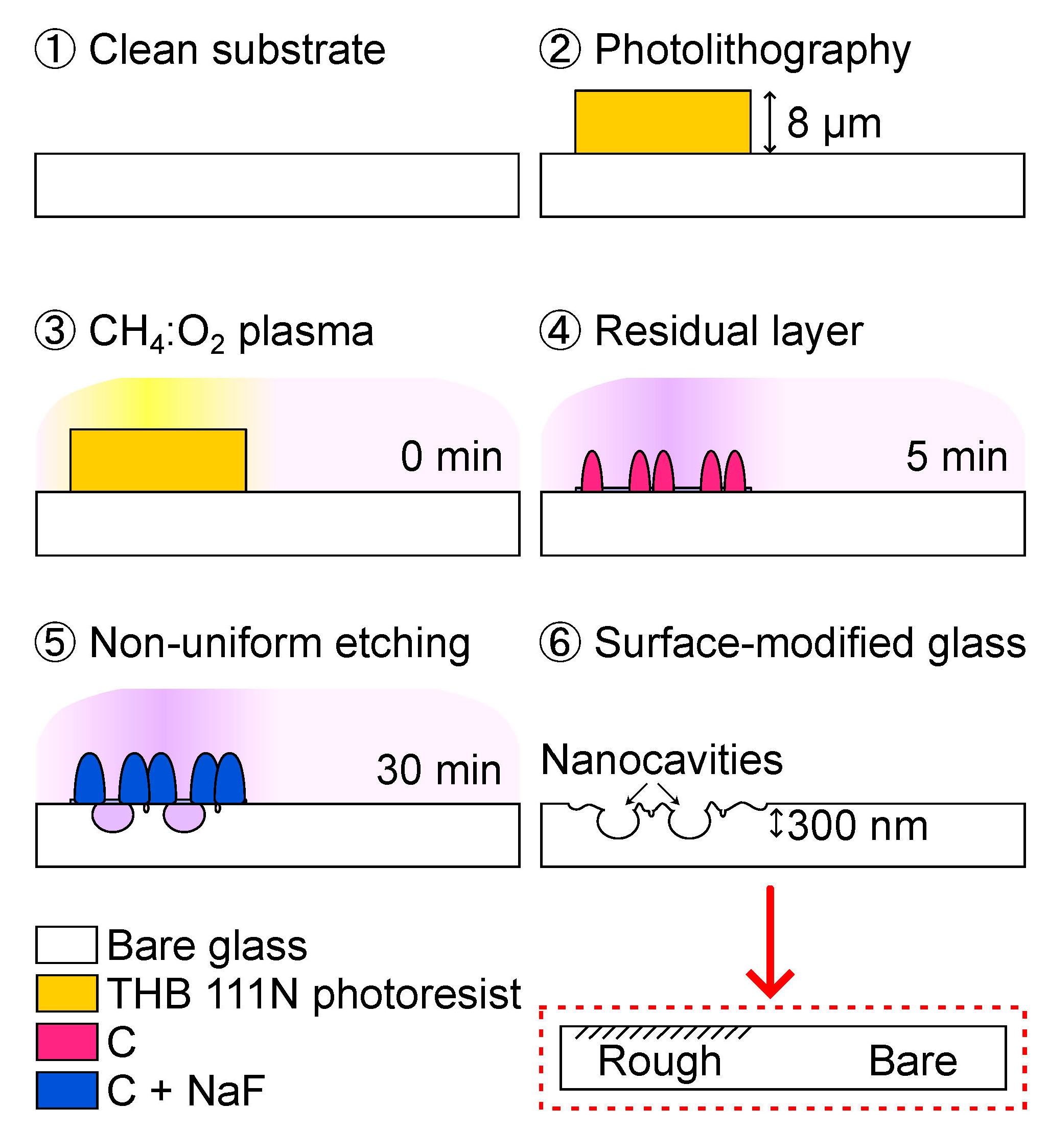
- Clean a soda-lime glass substrate in a piranha solution with a volume ratio of 3:1 for H2SO4 (96%):H2O2 (30%) for 15 min.
- Spin-coat a negative photoresist (THB 111N, JSR Corporation, Tokyo, Japan) at 2000 rpm for 30 s. Soft-bake in a convection oven at 393 K for 5 min. Transfer the pattern from the photomask using a mask aligner in vacuum-contact mode. Expose the sample to 365 nm UV light and deliver a total dose of 300 mJ/cm2. Develop the sample in a developer solution (AZ 300 MIF, Merck Electronic Materials Co., Ltd., Anseong, Republic of Korea) while gently shaking for 6 min. Hard-bake the sample on a hotplate for 10 min. Note: the glass with a photoresist layer undergoes a surface modification, and the photoresist layer is 8 μm thick.
- Use an RIE system (URL-100, ULTECH Co., Ltd., Daegu, Republic of Korea) for sample treatment at 200 mTorr with 10 sccm CF4 and 30 sccm O2. Plasma is produced by a 13.56 MHz RF power generator at 100 W. The sample chuck is continuously cooled to 288 K with a chiller.
- Carbon residuals can form on the photoresist-coated areas after RIE treatment for 5 min, initiating non-uniform etching reactions. The plasma glow color changes from white to light purple.
- Nanocavities are formed due to local masking effects caused by carbon residuals and the aggregation of less volatile components from the etching of the glass surface.
- Clean the RIE-treated sample in an ultrasonic bath with a photoresist stripper (STR-F, Hana Corporation Co., Ltd., Seongnam, Republic of Korea) for 1 h at 333 K. An arrow indicates the schematic for rough and bare glass used in the next section.
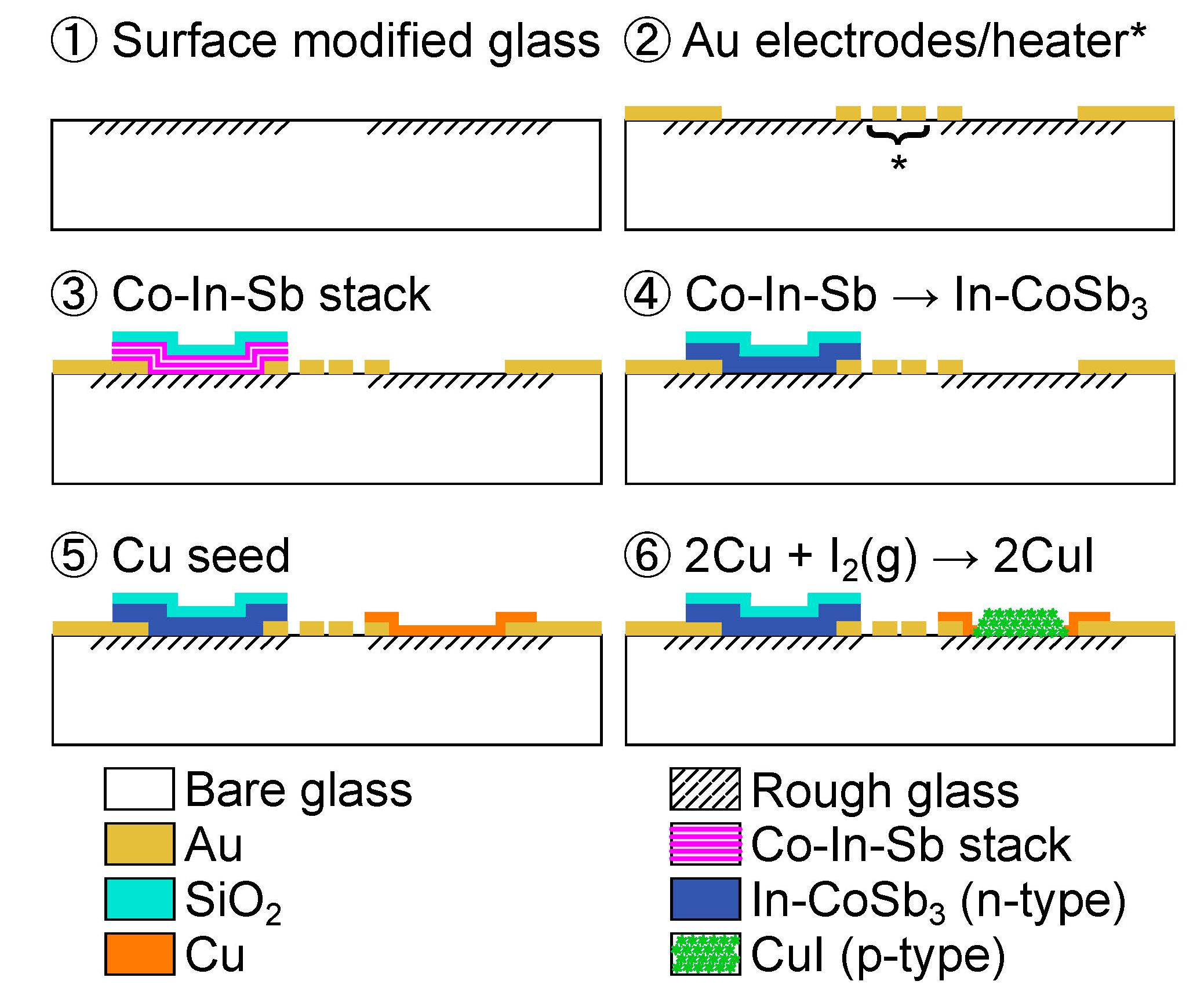
- Prepare a surface-modified glass according to the procedure in Figure 3.
- Pattern a sacrificial layer for lift-off of the Au electrode and heater with an AZ-nLOF-2070 photoresist 5 μm thick (Clariant Corporation, Somerville, NJ, USA). Deposit 70 nm Au (2.5 Å/s) on 30 nm of Cr (2.0 Å/s) by e-beam evaporation at 6 × 10⁻⁶ Torr. The heater location is shown by the asterisk (*).
- Pattern a photoresist layer for lift-off of the Co-In-Sb stack. Deposit seven cycles of a Co-In-Sb stack composed of 90 nm Sb (4.0 Å/s), 5 nm In (0.4 Å/s), and 9 nm Co (1.0 Å/s) on a 30 nm Cr adhesion layer. Deposit 250 nm SiO2 (1.5 Å/s) as a capping layer.
- Convert the Co-In-Sb stack into an In-doped CoSb3 layer by thermal annealing at 573 K for 20 min under ambient conditions.
- Pattern a photoresist layer for the lift-off of Cu. Deposit 160 nm Cu (4.0 Å/s) on a 3 nm Cr adhesion layer.
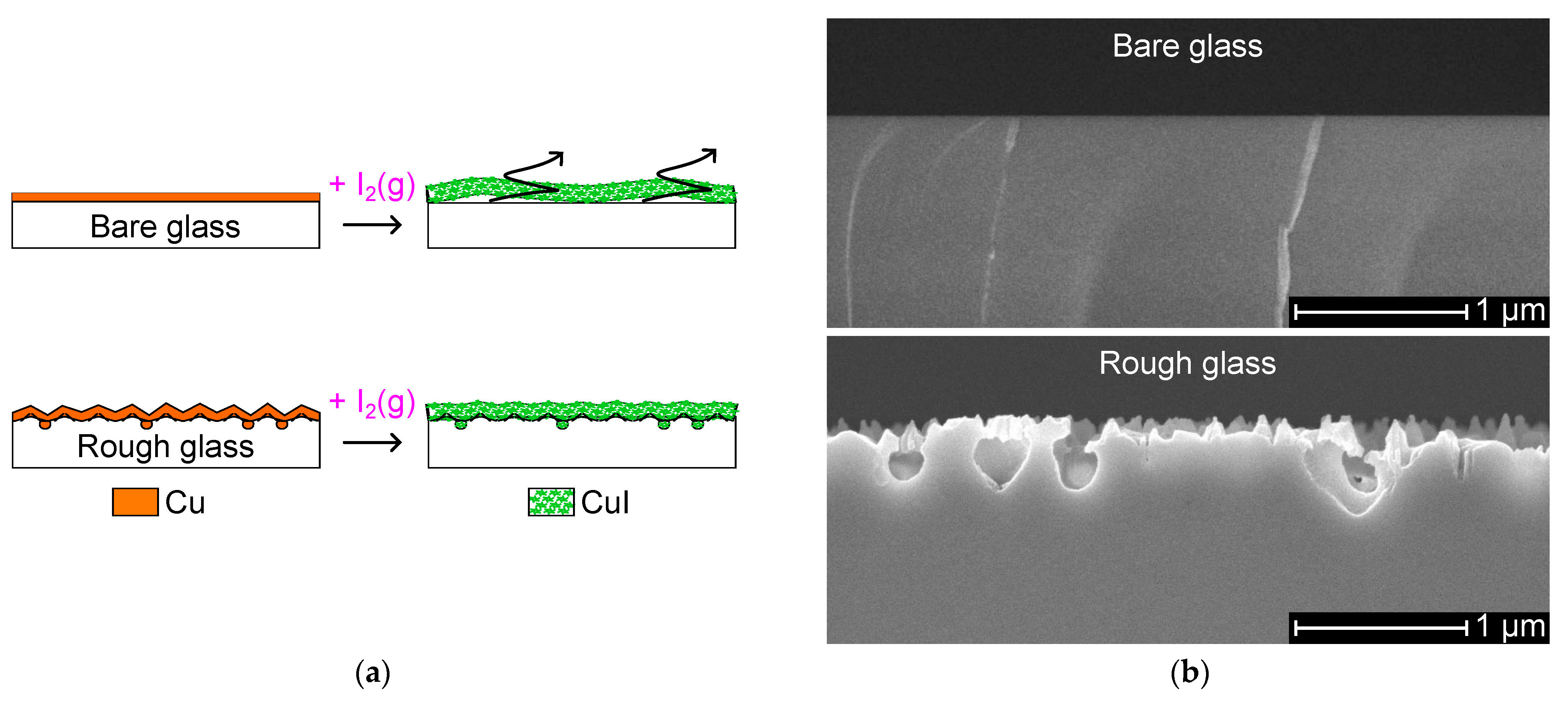
- Pattern a masking layer to expose only Cu on the textured glass with an AZ-10XT photoresist (520 cP) 7 μm thick (Clariant Corporation, Somerville, NJ, USA). Expose to iodine vapor in a sealed beaker on a hot plate at 373 K for 3 min under ambient conditions. Remove the photoresist.
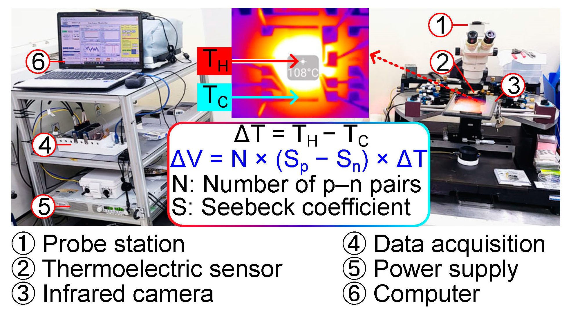
2.3. Measurement Setup
3. Results
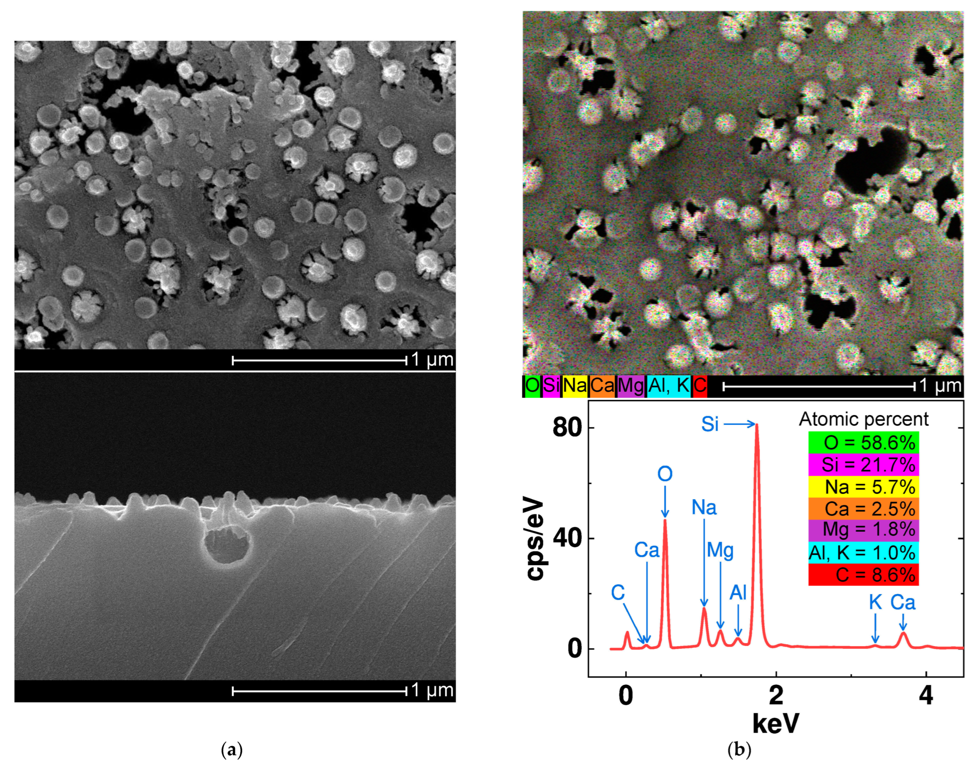
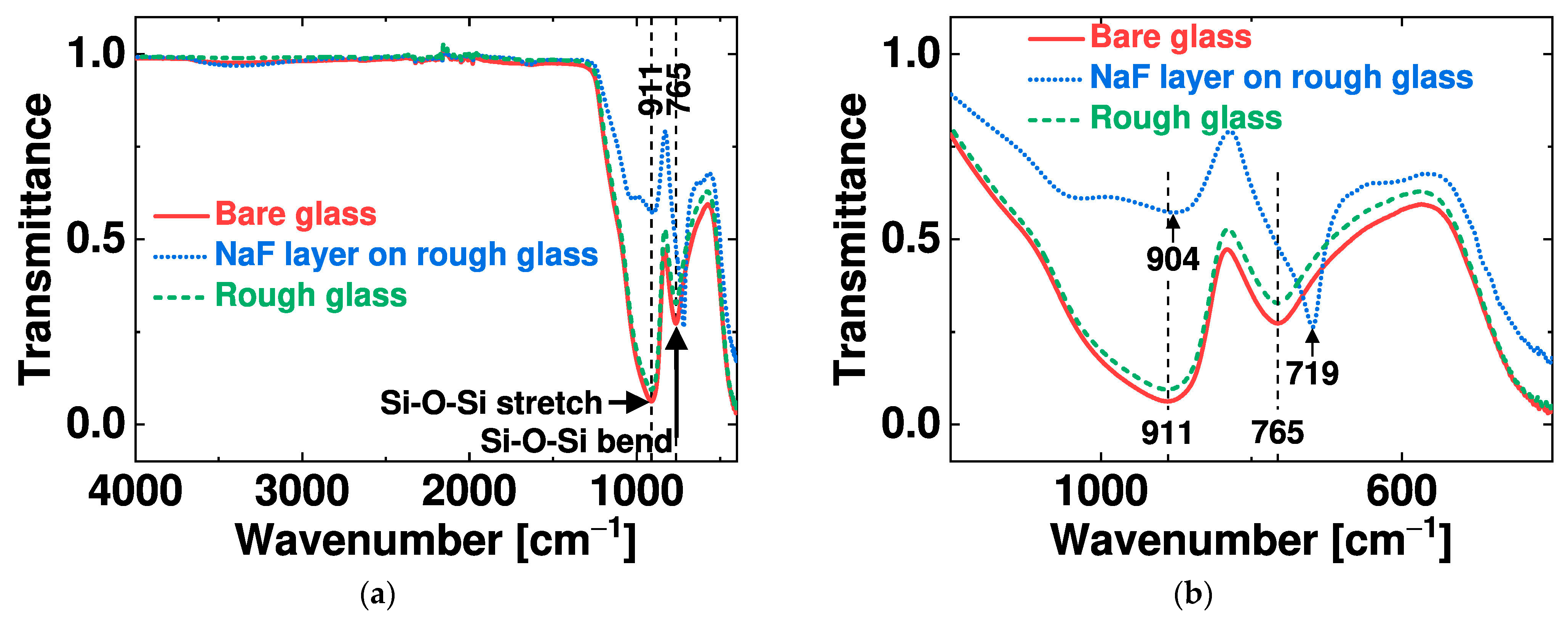
3.1. Characterization of the Glass Substrate
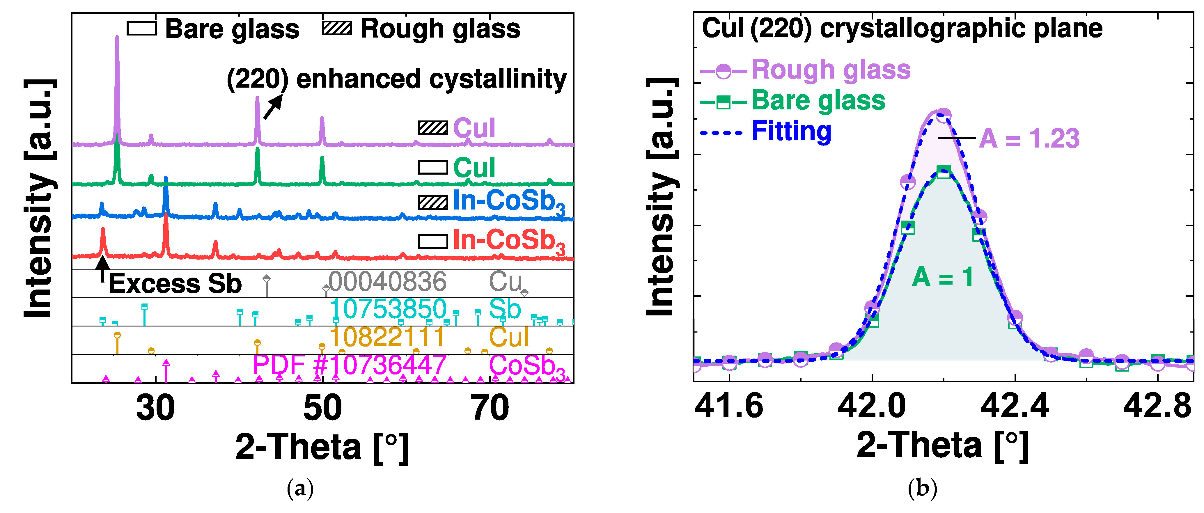
3.2. Characterization of Thermoelectric Layers
3.3. Test Results
4. Discussion
4.1. Mechanism for Rough Soda-Lime Glass with Nanocavities
4.2. Effects of the Surface Roughness
4.3. Adhesion Strength of the CuI Layer
4.4. Thermoelectric Response
5. Conclusions
Author Contributions
Funding
Data Availability Statement
Acknowledgments
Conflicts of Interest
References
- Zhang, Q.; Deng, K.; Wilkens, L.; Reith, H.; Nielsch, K. Micro-Thermoelectric Devices. Nat. Electron. 2022, 5, 333–347. [Google Scholar] [CrossRef]
- Freer, R.; Powell, A.V. Realising the Potential of Thermoelectric Technology: A Roadmap. J. Mater. Chem. C Mater. 2020, 8, 441–463. [Google Scholar] [CrossRef]
- Chudecka, M.; Lubkowska, A. Thermal Maps of Young Women and Men. Infrared Phys. Technol. 2015, 69, 81–87. [Google Scholar] [CrossRef]
- Webb, P. Temperatures of Skin, Subcutaneous Tissue, Muscle and Core in Resting Men in Cold, Comfortable and Hot Conditions. Eur. J. Appl. Physiol. Occup. Physiol. 1992, 64, 471–476. [Google Scholar] [CrossRef] [PubMed]
- Del Orbe Henriquez, D.; Cho, I.; Yang, H.; Choi, J.; Kang, M.; Chang, K.S.; Jeong, C.B.; Han, S.W.; Park, I. Pt Nanostructures Fabricated by Local Hydrothermal Synthesis for Low-Power Catalytic-Combustion Hydrogen Sensors. ACS Appl. Nano Mater. 2021, 4, 7–12. [Google Scholar] [CrossRef]
- Houlet, L.F.; Tajima, K.; Shin, W.; Itoh, T.; Izu, N.; Matsubara, I. Platinum Micro-Hotplates on Thermal Insulated Structure for Micro-Thermoelectric Gas Sensor. IEEJ Trans. Sens. Micromach. 2006, 126, 568–572. [Google Scholar] [CrossRef]
- Liu, A.; Zhu, H.; Kim, M.G.; Kim, J.; Noh, Y.Y. Engineering Copper Iodide (CuI) for Multifunctional p-Type Transparent Semiconductors and Conductors. Adv. Sci. 2021, 8, 2100546. [Google Scholar] [CrossRef] [PubMed]
- Jaldurgam, F.F.; Ahmad, Z.; Touati, F. Low-Toxic, Earth-Abundant Nanostructured Materials for Thermoelectric Applications. Nanomaterials 2021, 11, 895. [Google Scholar] [CrossRef]
- Posopa, N.; Sakulkalavek, A.; Chanlek, N.; Kaewkhao, J.; Sakdanuphab, R. Room-Temperature Rapid Synthesis of CuI Thin Films via Liquid Iodination Method. Superlattices Microstruct. 2020, 141, 106501. [Google Scholar] [CrossRef]
- Coroa, J.; Morais Faustino, B.M.; Marques, A.; Bianchi, C.; Koskinen, T.; Juntunen, T.; Tittonen, I.; Ferreira, I. Highly Transparent Copper Iodide Thin Film Thermoelectric Generator on a Flexible Substrate. RSC Adv. 2019, 9, 35384–35391. [Google Scholar] [CrossRef]
- Peng, W.; Li, L.; Yu, S.; Yang, P.; Xu, K.; Luo, W. High-Performance Flexible Transparent p-CuI Film by Optimized Solid Iodization. Vacuum 2021, 183, 109862. [Google Scholar] [CrossRef]
- Yamada, N.; Ino, R.; Ninomiya, Y. Truly Transparent P-Type γ-CuI Thin Films with High Hole Mobility. Chem. Mater. 2016, 28, 4971–4981. [Google Scholar] [CrossRef]
- Darnige, P.; Thimont, Y.; Presmanes, L.; Barnabé, A. Insights into Stability, Transport, and Thermoelectric Properties of Transparent p-Type Copper Iodide Thin Films. J. Mater. Chem. C Mater. 2023, 11, 630–644. [Google Scholar] [CrossRef]
- Ramu, A.T.; Cassels, L.E.; Hackman, N.H.; Lu, H.; Zide, J.M.O.; Bowers, J.E. Rigorous Calculation of the Seebeck Coefficient and Mobility of Thermoelectric Materials. J. Appl. Phys. 2010, 107, 83707. [Google Scholar] [CrossRef]
- Karthikeyan, V.; Theja, V.C.S.; De Souza, M.M.; Roy, V.A.L. Hierarchically Interlaced 2D Copper Iodide/MXene Composite for High Thermoelectric Performance. Phys. Status Solidi (RRL)—Rapid Res. Lett. 2022, 16, 2100419. [Google Scholar] [CrossRef]
- Qin, B.; Wang, D.; Zhao, L.D. Slowing down the Heat in Thermoelectrics. InfoMat 2021, 3, 755–789. [Google Scholar] [CrossRef]
- Hu, C.; Xia, K.; Fu, C.; Zhao, X.; Zhu, T. Carrier Grain Boundary Scattering in Thermoelectric Materials. Energy Environ. Sci. 2022, 15, 1406–1422. [Google Scholar] [CrossRef]
- Sun, Y.; Liu, Y.; Li, R.; Li, Y.; Bai, S. Strategies to Improve the Thermoelectric Figure of Merit in Thermoelectric Functional Materials. Front. Chem. 2022, 10, 865281. [Google Scholar] [CrossRef]
- Mehdizadeh Dehkordi, A.; Zebarjadi, M.; He, J.; Tritt, T.M. Thermoelectric Power Factor: Enhancement Mechanisms and Strategies for Higher Performance Thermoelectric Materials. Mater. Sci. Eng. R Rep. 2015, 97, 1–22. [Google Scholar] [CrossRef]
- Liu, Z.; Mao, J.; Liu, T.H.; Chen, G.; Ren, Z. Nano-Microstructural Control of Phonon Engineering for Thermoelectric Energy Harvesting. MRS Bull. 2018, 43, 181–186. [Google Scholar] [CrossRef]
- Yang, C.; Souchay, D.; Kneiß, M.; Bogner, M.; Wei, H.M.; Lorenz, M.; Oeckler, O.; Benstetter, G.; Fu, Y.Q.; Grundmann, M. Transparent Flexible Thermoelectric Material Based on Non-Toxic Earth-Abundant p-Type Copper Iodide Thin Film. Nat. Commun. 2017, 8, 16076. [Google Scholar] [CrossRef] [PubMed]
- Jacob, U.; Vancea, J.; Hoffmann, H. Surface-Roughness Contributions to the Electrical Resistivity of Polycrystalline Metal Films. Phys. Rev. B 1990, 41, 11852. [Google Scholar] [CrossRef] [PubMed]
- Hof, L.A.; Ziki, J.A.; Jiang, H.; Nguyen, N.-T. Micro-Hole Drilling on Glass Substrates—A Review. Micromachines 2017, 8, 53. [Google Scholar] [CrossRef]
- Hein, E.; Fox, D.; Fouckhardt, H. Glass Surface Modification by Lithography-Free Reactive Ion Etching in an Ar/CF4-Plasma for Controlled Diffuse Optical Scattering. Surf. Coat. Technol. 2011, 205, S419–S424. [Google Scholar] [CrossRef]
- Mazurczyk, R.; Mansfield, C.D. Introduction to Glass Microstructuring Techniques. Methods Mol. Biol. 2013, 949, 125–140. [Google Scholar] [CrossRef] [PubMed]
- Bansal, N.P.; Doremus, R.H. Handbook of Glass Properties; Elsevier BV: Amsterdam, The Netherlands, 2013; pp. 1–680. [Google Scholar] [CrossRef]
- Panama, G.; Jo, M.; Shim, S.S.; Kim, M.S.; Lee, S.S. Hydrogen Sensor with a Thick Catalyst Layer Anchored on Soda-Lime Glass. Int. J. Hydrog. Energy 2023, 55, 875–881. [Google Scholar] [CrossRef]
- Iacona, F.; Casella, G.; La Via, F.; Lombardo, S.; Raineri, V.; Spoto, G. Structural Properties of Fluorinated SiO2 Thin Films. Microelectron. Eng. 2000, 50, 67–74. [Google Scholar] [CrossRef]
- Zhu, Y.; Li, Y.; Ding, H.; Lu, A.; Li, Y.; Ji, X.; Zhang, Y.; Wang, C. Vibrational and Structural Insight into Silicate Minerals by Mid-Infrared Absorption and Emission Spectroscopies. Phys. Chem. Miner. 2022, 49, 6. [Google Scholar] [CrossRef]
- Chen, G.; Zhang, J.; Yang, S. Fabrication of Hydrophobic Fluorinated Amorphous Carbon Thin Films by an Electrochemical Route. Electrochem. Commun. 2008, 10, 7–11. [Google Scholar] [CrossRef]
- Kennedy, J.V.; Murmu, P.P.; Karthik, V.; Liu, Z.; Jovic, V.; Mori, T.; Yang, W.L.; Smith, K.E. Influence of Carrier Density and Energy Barrier Scattering on a High Seebeck Coefficient and Power Factor in Transparent Thermoelectric Copper Iodide. ACS Appl. Energy Mater. 2020, 3, 10037–10044. [Google Scholar] [CrossRef]
- Zheng, Z.H.; Fan, P.; Zhang, Y.; Luo, J.T.; Huang, Y.; Liang, G.X. High-Performance In Filled CoSb3 Nano Thin Films Fabricated by Multi-Step Co-Sputtering Method. J. Alloys Compd. 2015, 639, 74–78. [Google Scholar] [CrossRef]
- Wen, P.F.; Li, P.; Zhang, Q.J.; Ruan, Z.W.; Liu, L.S.; Zhai, P.C. Effects of Annealing on Microstructure and Thermoelectric Properties of Nanostructured CoSb3. J. Electron. Mater. 2012, 42, 1443–1448. [Google Scholar] [CrossRef]
- Karouta, F. A Practical Approach to Reactive Ion Etching. J. Phys. D Appl. Phys. 2014, 47, 233501. [Google Scholar] [CrossRef]
- Metwalli, E.E.; Pantano, C.G. Reactive Ion Etching of Glasses: Composition Dependence. Nucl. Instrum. Methods Phys. Res. B 2003, 207, 21–27. [Google Scholar] [CrossRef]
- Beena Unni, A.; Winkler, R.; Duarte, D.M.; Chat, K.; Adrjanowicz, K. Influence of Surface Roughness on the Dynamics and Crystallization of Vapor-Deposited Thin Films. J. Phys. Chem. B 2022, 126, 8072–8079. [Google Scholar] [CrossRef] [PubMed]
- Faustino, B.M.M.; Gomes, D.; Faria, J.; Juntunen, T.; Gaspar, G.; Bianchi, C.; Almeida, A.; Marques, A.; Tittonen, I.; Ferreira, I. CuI P-Type Thin Films for Highly Transparent Thermoelectric p-n Modules. Sci. Rep. 2018, 8, 6867. [Google Scholar] [CrossRef] [PubMed]
- Zhang, K.X.; Wang, S.W.; Zhang, Y.W.; Yi, L.X. The Influence of Thickness on Morphology and Iodine Decomposition in Copper(I) Iodide Film. Thin Solid Films 2021, 733, 138827. [Google Scholar] [CrossRef]
- Lin, G.; Zhao, F.; Zhao, Y.; Zhang, D.; Yang, L.; Xue, X.; Wang, X.; Qu, C.; Li, Q.; Zhang, L. Luminescence Properties and Mechanisms of CuI Thin Films Fabricated by Vapor Iodization of Copper Films. Materials 2016, 9, 990. [Google Scholar] [CrossRef]
- Mulla, R.; Jones, D.R.; Dunnill, C.W. Thin-Films on Cellulose Paper to Construct Thermoelectric Generator of Promising Power Outputs Suitable for Low-Grade Heat Recovery. Mater. Today Commun. 2021, 29, 102738. [Google Scholar] [CrossRef]
- Kapton®, EN. Available online: https://www.dupont.com/electronics-industrial/kapton-en.html (accessed on 24 December 2023).
- Bae, E.J.; Kim, J.; Han, M.; Kang, Y.H. Precision Doping of Iodine for Highly Conductive Copper(I) Iodide Suitable for the Spray-Printable Thermoelectric Power Generators. ACS Mater. Lett. 2023, 5, 2009–2018. [Google Scholar] [CrossRef]
- Maji, T.; Rousti, A.M.; Kazi, A.P.; Drew, C.; Kumar, J.; Christodouleas, D.C. Wearable Thermoelectric Devices Based on Three-Dimensional PEDOT:Tosylate/CuI Paper Composites. ACS Appl. Mater. Interfaces 2021, 13, 46919–46926. [Google Scholar] [CrossRef] [PubMed]
- Ao, D.; Li, F.; Chen, Y.; Luo, J.; Liang, G.; Zheng, Z.; Zhang, X.-H.; Fan, P. CoSb3-Based Thin-Film Thermoelectric Devices with High Performance Via Electrode Optimization. ACS Appl. Energy Mater. 2021, 4, 5265–5273. [Google Scholar] [CrossRef]
- Kaushik, D.K.; Selvaraj, M.; Ramu, S.; Subrahmanyam, A. Thermal Evaporated Copper Iodide (CuI) Thin Films: A Note on the Disorder Evaluated through the Temperature Dependent Electrical Properties. Sol. Energy Mater. Sol. Cells 2017, 165, 52–58. [Google Scholar] [CrossRef]
- Almasoudi, M.; Saeed, A.; Salah, N.; Alshahrie, A.; Hasan, P.M.Z.; Melaibari, A.; Koumoto, K. CuI: A Promising Halide for Thermoelectric Applications below 373 K. ACS Appl. Energy Mater. 2022, 5, 10177–10186. [Google Scholar] [CrossRef]


| Material | Thickness [nm] | CuI Precursor | Area 1 [mm2] | Substrate | S 1 [mV/K] | Reference |
|---|---|---|---|---|---|---|
| CuI | 300 | Cu, I2(s) | - | PET | 0.17 | [21] |
| CuI | 325 | 100 nm Cu, I2(s) | 12 × 12 | 1000 μm glass | 0.29 | [13] |
| CuI/GZO | 302/306 | 60 nm Cu, I2(s) | 10 × 30 | 50 μm Kapton | 0.09 | [10] |
| CuI/Bi | 1400/200 | 200 nm Cu, I2(g) | 20 × 12 | 100 μm paper | 0.18 | [40] |
| CuI/ITO | 550/- | CuI + I2 solution | 45 × 20 | ITO/polyimide | 0.26 | [42] |
| CuI/Monel 2 | 3/0.5 × 106 | CuSO4, NaI sol. | 13 × 13 | 2.75 mm paper | 0.23 | [43] |
| P-N CoSb3 | 200/185 | Ti, In, CoSb3 | 8 × 6 | 150 μm Kapton | 0.34 | [44] |
| CuI/In-CoSb3 | 1000/750 | 160 nm Cu, I2(g) | 3 × 0.14 | Soda-lime glass | 0.33 | This work |
Disclaimer/Publisher’s Note: The statements, opinions and data contained in all publications are solely those of the individual author(s) and contributor(s) and not of MDPI and/or the editor(s). MDPI and/or the editor(s) disclaim responsibility for any injury to people or property resulting from any ideas, methods, instructions or products referred to in the content. |
© 2024 by the authors. Licensee MDPI, Basel, Switzerland. This article is an open access article distributed under the terms and conditions of the Creative Commons Attribution (CC BY) license (https://creativecommons.org/licenses/by/4.0/).
Share and Cite
Panama, G.; Lee, S.S. Thermoelectric Sensor with CuI Supported on Rough Glass. Nanomaterials 2024, 14, 105. https://doi.org/10.3390/nano14010105
Panama G, Lee SS. Thermoelectric Sensor with CuI Supported on Rough Glass. Nanomaterials. 2024; 14(1):105. https://doi.org/10.3390/nano14010105
Chicago/Turabian StylePanama, Gustavo, and Seung S. Lee. 2024. "Thermoelectric Sensor with CuI Supported on Rough Glass" Nanomaterials 14, no. 1: 105. https://doi.org/10.3390/nano14010105
APA StylePanama, G., & Lee, S. S. (2024). Thermoelectric Sensor with CuI Supported on Rough Glass. Nanomaterials, 14(1), 105. https://doi.org/10.3390/nano14010105