Article

Broadband Optical Properties of Bi2Se3

by
Georgy A. Ermolaev
1,
Ivan S. Vyslanko
1,
Andrey P. Tselin
1,2,
Marwa A. El-Sayed
1,3,
Mikhail K. Tatmyshevskiy
1,
Aleksandr S. Slavich
1,
Dmitry I. Yakubovsky
1,
Mikhail S. Mironov
1,
Arslan B. Mazitov
1,
Amir Eghbali
1,
Daria A. Panova
1,
Roman I. Romanov
4,
Andrey M. Markeev
1,
Ivan A. Kruglov
1,5,
Sergey M. Novikov
1,
Andrey A. Vyshnevyy
1,
Aleksey V. Arsenin
1,6 and
Valentyn S. Volkov
1,*
1
Center for Photonics and 2D Materials, Moscow Institute of Physics and Technology, 9 Institutsky Lane, Dolgoprudny 141700, Russia
2
Photonics and Quantum Materials Department, Skolkovo Institute of Science and Technology, 3 Nobel Str., Moscow 143026, Russia
3
Department of Physics, Faculty of Science, Menoufia University, Shebin El-Koom 32511, Egypt
4
Department of Solid State Physics and Nanosystems, National Research Nuclear University MEPhI (Moscow Engineering Physics Institute), 31 Kashirskoe Sh., Moscow 115409, Russia
5
Center of Fundamental and Applied Research, Dukhov Research Institute of Automatics (VNIIA), 22 Suschevskaya Str., Moscow 127055, Russia
6
Laboratory of Advanced Functional Materials, Yerevan State University, 1 Alek Manukyan Str., Yerevan 0025, Armenia
*
Author to whom correspondence should be addressed.
Nanomaterials 2023, 13(9), 1460; https://doi.org/10.3390/nano13091460
Submission received: 8 March 2023 / Revised: 18 April 2023 / Accepted: 21 April 2023 / Published: 25 April 2023
(This article belongs to the Special Issue 2D Materials for Advanced Sensors: Fabrication and Applications)

Abstract

:
Materials with high optical constants are of paramount importance for efficient light manipulation in nanophotonics applications. Recent advances in materials science have revealed that van der Waals (vdW) materials have large optical responses owing to strong in-plane covalent bonding and weak out-of-plane vdW interactions. However, the optical constants of vdW materials depend on numerous factors, e.g., synthesis and transfer method. Here, we demonstrate that in a broad spectral range (290–3300 nm) the refractive index n and the extinction coefficient k of Bi2Se3 are almost independent of synthesis technology, with only a ~ 10% difference in n and k between synthesis approaches, unlike other vdW materials, such as MoS2, which has a ~ 60% difference between synthesis approaches. As a practical demonstration, we showed, using the examples of biosensors and therapeutic nanoparticles, that this slight difference in optical constants results in reproducible efficiency in Bi2Se3-based photonic devices.

1. Introduction

High-refractive-index materials are the core of modern nanophotonics [1,2]. In particular, the real part n of the complex refractive index n ˜ determines the photonic devices’ footprint, which scales as λ / n , where λ is a free space wavelength of light [3,4]. Moreover, the device performance is also highly dependent on n [5]. Hence, even a minor increase in the refractive index has a significant impact on nanophotonics [1]. However, classical high-refractive-index materials (TiO2, GaP, Si, and Ge) offer a limited range of available refractive indices, and these typically fall below 4 [2,6,7,8]. It is thus necessary to search for new optical materials with large optical responses [1].
The appearance of graphene and other two-dimensional (2D) and layered materials [9,10,11] has led to the development of a novel materials platform, usually referred to as van der Waals (vdW) materials [12,13]. To date, there are more than 5000 potential vdW crystal structures which provide diverse optical responses [14] and can be employed together with or fully independently of bulk materials. One of the most promising is a family of transition metal dichalcogenides (TMDCs), which includes MoS2, WS2, MoSe2, and WSe2 [12,15,16,17,18]. Due to their pronounced in-plane excitonic effects, they offer previously unimaginable optical constants with in-plane refractive indices exceeding 4 [12,19,20]. As a result, numerous studies consider vdW materials to be essential building blocks for next-generation nanophotonics [1,4,12,21]. However, industrial implementation requires standardized optical responses, i.e., sample-to-sample variations in optical properties should be very low. By contrast, the optical constants of vdW materials depend on numerous factors [22,23,24,25,26], among which the most influential are the dielectric environment and the synthesis method. For example, recent research [23] has demonstrated that optical constants vary dramatically among differently synthesized samples of monolayer MoS2. At λ = 750 nm, the refractive indices n of exfoliated, epitaxial, and chemical vapor deposition-grown MoS2 are equal to 3.16, 4.02, and 5.16, respectively [23]. This is a more than 60% variation in optical constants, which greatly impedes the commercial viability of TMDCs. Furthermore, the considerable differences between the optical constants of differently synthesized samples is not only problematic for 2D materials, but for bulk crystals too, as can be seen from the comparison of dielectric functions of chemical vapor deposition-grown [27] and exfoliated [12] MoS2 (Figure A1). Therefore, vdW materials with synthesis-independent optical properties are in high demand.
To address this issue, we focused on vdW topological insulators such as Bi2Se3, Bi2S3, Bi2Te3, and Sb2Te3 [28,29,30,31,32,33,34]. Their topological nature has attracted renewed interest in their electronic and optical properties [32,35,36,37,38,39,40,41]. More importantly, they demonstrate an even stronger optical response than TMDCs with a refractive index above 5 [32,40,42,43]. This enables, for example, the realization of pronounced Mie resonances with high-order multipoles [32]. Therefore, their optical constants are of great interest. Finally, one might assume that the optical responses of vdW topological insulators is less dependent on the synthesis process than those of TMDCs because of the topological protection of their topological surface states [44].
In this study, we investigated the dependence of the broadband optical properties of Bi2Se3, which is a typical vdW topological insulator, on the synthesis method. The comparison of spectroscopic ellipsometry results and first-principle computations together with the literature database reveal that Bi2Se3 has synthesis-independent optical constants. Additionally, we determined the broadband (290–3300 nm) refractive index and extinction coefficient. Our findings show that Bi2Se3 has a high refractive index ( n ~ 5) and extinction coefficient ( k > 0.1) for a wide spectral interval, which makes Bi2Se3 a promising material for a wide range of photonic applications.

2. Materials and Methods

2.1. Materials

Full area coverage Bi2Se3 thin film was purchased from SixCarbon (6CarbonTechnology, Shenzhen, China), where the sample was synthesized via the chemical vapor deposition (CVD) method on a silicon substrate with silicon dioxide.

2.2. Raman Characterization

A Horiba LabRAM HR Evolution confocal scanning Raman microscope (Horiba Ltd., Kyoto, Japan) was employed for the acquisition of the Raman spectra of the Bi2Se3. All measurements were carried out under linearly polarized excitation at free space wavelengths of 532 nm and 632.8 nm with a 1800 lines/mm diffraction grating and a 100× objective with a numerical aperture (NA) of 0.90. The spot diameter was approximately 0.9 µm. The Raman spectra were recorded with an integration time of 10 s.

2.3. Spectroscopic Ellipsometry Characterization

A variable-angle spectroscopic ellipsometer (VASE, J.A. Woollam Co., Lincoln, NE, USA) was utilized to measure the broadband optical constants of the Bi2Se3. The measurements were performed at multiple incident angles from 50° to 70° in 5° steps, and over a broad spectral interval from 290 nm to 3300 nm. For the ellipsometry spectra analysis, we employed WVASE software, provided by the producer. We described the Bi2Se3 sample using a four-layer model: roughness layer, Bi2Se3 layer, silicon dioxide (SiO2), and silicon (Si) substrate. The thicknesses of the layers were 21.7 nm (for the roughness layer), 44.4 nm (for the Bi2Se3 layer), 265.7 nm (for the SiO2 layer), and a semi-infinite layer for the silicon. In order to account for the surface roughness, we followed a standard approach [45] which involved introducing the Bruggeman effective medium approximation layer with equal fractions of air and investigating the Bi2Se3 material. In addition, despite the uniaxial anisotropy of the Bi2Se3 [12], we used an isotropic model for the Bi2Se3 since ellipsometry is almost insensitive to the out-of-plane component because of the high in-plane refractive index, which significantly decreases the interaction between the light electric field and the out-of-plane dielectric function of the film.

2.4. Reflectance Measurements

The reflectance spectrum ( λ =  450–950 nm) of the Bi2Se3 sample was measured using a Biolam M-1 optical microscope (LOMO, Saint Petersburg, Russia) equipped with a 24 V, 100 W halogen light source and a QE65000 spectrometer (Ocean Optics, Dunedin, FL, USA).

2.5. First-Principle Calculations

The optical constants of the Bi2Se3 were calculated using the GW@DFT approach implemented in the VASP package [46]. First, the atomic positions of the crystal ( a = b = 0.4143   nm and c = 2.8636   nm) [47] were relaxed until the converged interatomic forces were less than 10−2 eV/nm, and the unit cell was kept fixed. Next, we obtained ground-state one-electron wavefunctions using the density functional theory (DFT) and used them to initialize the GW routines. Finally, we calculated the imaginary and real parts of the frequency-dependent dielectric function within the GW approximation and derived the refractive indices and extinction coefficients of the material. The cutoff energy for the plane-wave basis set was 500 eV, while the first Brillouin zone was sampled with a Γ-centered 18 × 18 × 3 grid. The exchange correlation effects were described with a generalized gradient approximation (Perdew–Burke–Ernzerhof functional) [48], and the behavior of the wavefunctions in the core region was reconstructed with a projector augmented wave pseudopotentials [49].

2.6. Optical Visualization

The optical images of the Bi2Se3 samples were recorded using an optical microscope (Nikon LV150L, Tokyo, Japan).

2.7. Atomic-Force Microscopy

The surface topography of the Bi2Se3 films was examined using an atomic force microscope (NT-MDT Ntegra) operated in a semi-contact mode. AFM scanning was performed in air using HA_NC ETALON silicon tips (TipsNano, Tallinn, Estonia) with a tip-tapping resonant frequency of around 140 kHz and a spring constant of 3.5 N/m. The quantitative analysis was carried out using Gwyddion software (www.gwyddion.net; accessed on 1 January 2022).

2.8. X-ray Photoelectron Spectroscopy

The chemical state and composition were analyzed via X-ray photoelectron spectroscopy (XPS) using a Theta Probe spectrometer under high-vacuum conditions (base pressure < 2 × 10⁻⁹ mbar) with a monochromatic Al-Kα X-ray source (1486.6 eV). The photoelectron spectra were acquired using the fixed analyzer transmission (FAT) mode with 50 eV pass energy. The spectrometer energy scale was calibrated on the Au4f7/2 line (84.0 eV). The XPS spectra were acquired using charge-compensation under the pressure of ~10−7 mbar to avoid sample charging. For the elemental composition XPS analysis, Scofield’s Factors were employed in the calculations.

3. Results and Discussion

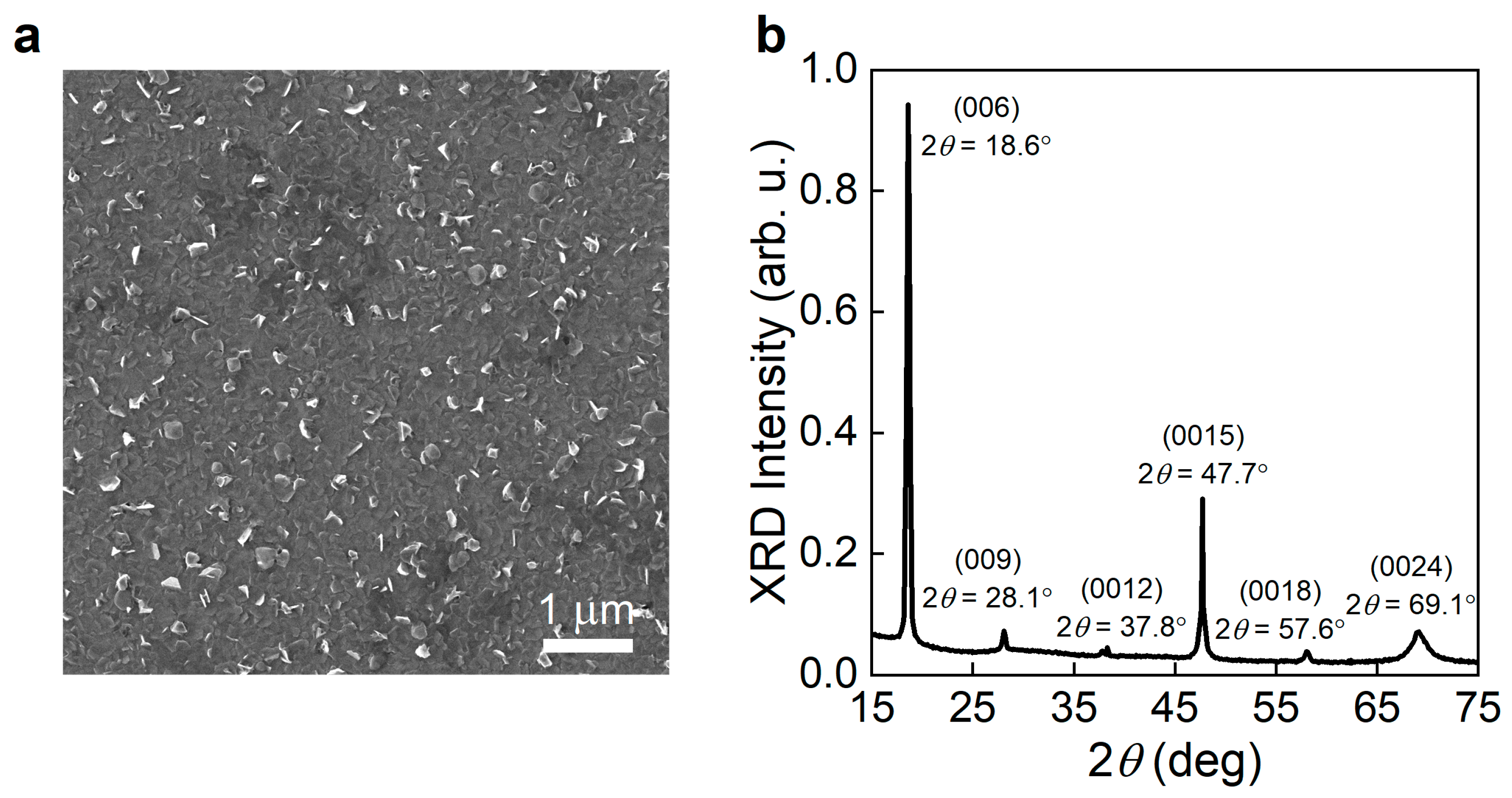
3.1. Sample Characterization

Bi2Se3 has a rhombohedral phase crystal structure with quintuple layers (Figure 1a). Our Bi2Se3 thin film was prepared using the chemical vapor deposition (CVD) method and, therefore, had a uniform substrate coverage, confirmed by optical microscopy (Figure 1b). From the optical image in Figure 1b, one can notice that the synthesized sample has a roughness, similar to other Bi2Se3 samples grown using CVD [50,51]. In order to obtain a qualitative estimate of the roughness, we measured the sample surface with an atomic-force microscope (Figure 1c). The AFM image yielded a root mean square roughness of 26 nm. After that, we verified the stoichiometry of the samples using X-ray photoemission spectroscopy (XPS) (Figure 1d,e). The XPS signal in Figure 1d,e shows a rich spectrum with Bi- and Se-related peaks, and a quantitative XPS analysis based on Bi4f and Se3d showed that the stoichiometry of the film reached ~ 43%:57%, close to the expected 40%:60% (2 Bi: 3 Se) [52,53,54,55]. According to the previous studies of Bi2Se3, the peak Se0 (Figure 1e) indicates elemental selenium (Se) [55,56,57]. Additionally, we performed Raman spectroscopy (Figure 1f,g) at two excitation wavelengths: 532 nm (Figure 1f) and 632.8 nm (Figure 1g). Both spectra have two pronounced Raman peaks at 131.3 cm−1 and 174.3 cm−1 for λ = 532 nm and 131.9 cm−1 and 174.8 cm−1 for λ = 632.8 nm (Figure 1f,g). A comparison with Bi2Se3 data from the literature allowed us to assign the first peak with the E g 2 phonon mode and the second peak with the A 1 g 2 phonon mode, and their positions are very close to those reported for Bi2Se3 ( A 1 g 2   ~ 131 cm−1 and E g 2   ~ 174 cm−1) with a thickness above 20 nm [58]. In addition, we performed scanning electron microscopy (SEM) and X-ray diffraction (XRD), as is shown in Figure A2. The SEM image in Figure A2a confirms the morphology of our sample surface as observed using atomic-force microscopy (Figure 1c), and the XRD pattern (Figure A2b) gives additional verification of Bi2Se3 crystal structure: the XRD peaks at around 9.3°, 18.6°, 28.1°, 37.8°, 47.7°, 57.6°, and 69.1° correspond to the (003), (006), (009), (0012), (0015), (0018), and (0021) crystallographic planes of the Bi2Se3, respectively [59]. In addition, we would like to note that the XPS spectra (Figure 1d,e) demonstrate the slight oxidation of the sample. However, other techniques, such as Raman spectroscopy (Figure 1f,g) and XRD (Figure A2b), show only the presence of Bi2Se3, which additionally confirms that the sample was only slightly oxidized. Hence, this preliminary sample characterization confirmed that our sample was Bi2Se3 and gives additional information about its roughness, which should be about 26 nm, and its thickness, which should be more than 20 nm.

3.2. Spectrocopic Ellipsometry of Bi2Se3

To obtain the broadband optical properties of the Bi2Se3, we measured the spectroscopic ellipsometry of our sample at several incident angles ( θ = 50–70°) in a broad wavelength range ( λ = 290–3300 nm). The resulting spectra of ellipsometric parameters Ψ and Δ are plotted in Figure 2a,b. Since ellipsometry is a very accurate technique [60] that “feels” a system’s nonidealities, we included in the optical model an effective medium approximation (EMA) layer [45,61] on top of the Bi2Se3 film to account for the surface roughness (Figure 1b,c). We also assumed a negligible optical response from the Bi2Se3 oxide and the surface conductive layer, and therefore did not include it in the optical model. Our ellipsometry analysis started with a point-by-point conversion approach [62]. We then used the results from the first step for the Lorentz oscillator description of the optical constants of the Bi2Se3 (Figure 2c,d). We would like to note that unlike those of other semiconducting layered materials, the Bi2Se3 optical response is better described via Lorentz oscillators than via Tauc-Lorentz oscillators [63] since Bi2Se3 is a narrow bandgap ( E g   0.3 eV) semiconductor [34]. In other words, the lowest energy incident photon has 0.376 eV energy, which is much larger than the bandgap E g = 0.3 eV of Bi2Se3. We also confirmed this bandgap value with band structure computations (the inset in Figure 2c) using density functional theory. Furthermore, to validate the Bi2Se3 optical constants in Figure 2c,d and their predictive capabilities, we recorded the reflectance spectrum of our sample (the inset in Figure 2d) and compared it with the transfer matrix calculations [64] based on the refractive indices and extinction coefficients presented in Figure 2c,d. Therefore, our assumptions concerning a negligible optical response from the oxide layer and the EMA approach for roughness are valid because they were double-checked against the first-principle calculations and reflectance measurements, and there was good agreement between the AFM roughness of 26 nm and the effective ellipsometry roughness of 21.7 nm.
In addition to this, we compared the resulting dielectric function of our CVD-grown sample with the first-principle calculations and dielectric function of molecular beam epitaxy (MBE)-grown Bi2Se3, reported by Fang and colleagues [40]. Interestingly, our recent publications [12,65] have shown that DFT dielectric function coincides with the optical response of monocrystals (an almost perfect match for n and a qualitative match with k), which in the case of layered materials are usually prepared using the exfoliation technique [66]. Hence, we can safely assume that DFT optical constants correspond with exfoliated Bi2Se3. In this case, the perfect match between the CVD-grown, exfoliated, and MBE-grown Bi2Se3 (Figure 2c,d) implies that the Bi2Se3 optical response is almost synthesis-invariant, unlike those of other vdW materials [23]. This property makes Bi2Se3 a promising vdW material for commercial use because its optical properties are reproducible.
In addition to CVD and MBE technologies, Bi2Se3 can also be synthesized using numerous other methods, e.g., solvothermal [67] and sonochemical [68] methods and mechanical exfoliation [69]. Unfortunately, for most synthesis methods, it is hard to find optical constants for comparison because researchers now focus primarily on the electronic properties of topological states rather than the optics of Bi2Se3. Nevertheless, the CVD and MBE methods are the most popular and well-developed for synthesizing two-dimensional and layered materials and, therefore, the most important for the scientific community. Additionally, we provide first-principle computations, which give optical constants close to those of the exfoliated samples [12]. Hence, we can conclude that first-principle computations yield optical constants for exfoliated Bi2Se3, expanding our comparison to the three synthesis methods (CVD, MBE, and exfoliated) and confirming the synthesis-independent optical response of Bi2Se3.

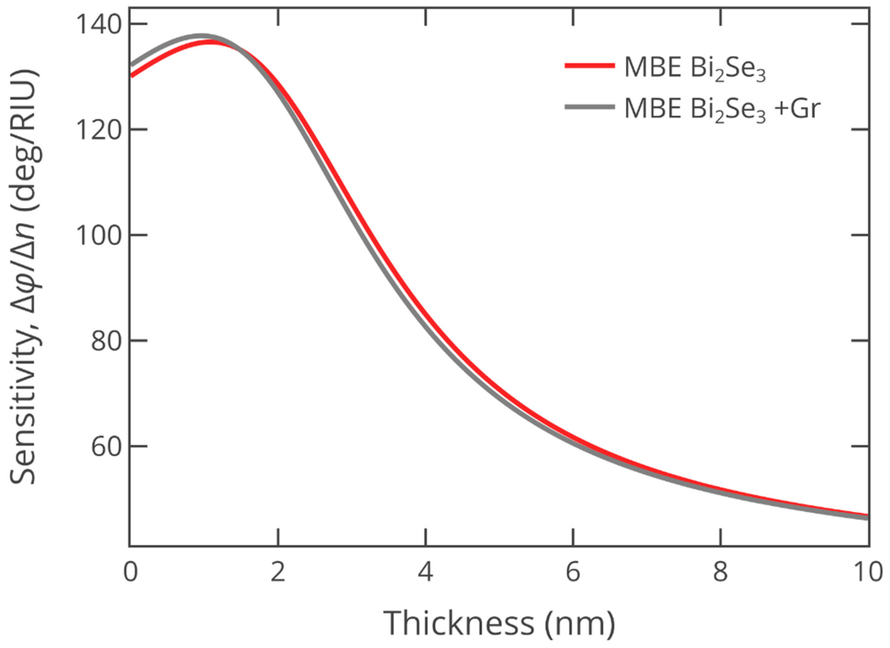
3.3. Applications of Bi2Se3

To demonstrate the invariant performance of Bi2Se3-based photonic devices, we chose two applications: a surface plasmon resonance (SPR) biosensor [70] and the heating of nanoparticles for cancer treatment [21]. Performance-invariance is imperative for the reliable industrial implementation of Bi2Se3.
We commence with a Bi2Se3-based SPR biosensor. In a common approach [70] to SPR-sensitivity enhancement, one usually deposits vdW materials on top of gold (or other plasmonic material) in a biosensor using the Kretschmann scheme (the inset in Figure 3b) [71]. The benefit of the added vdW material is twofold: (i) it increases the sensitivity of the biosensor; (ii) it enhances the immobilization efficiency of the detected molecules. Since Bi2Se3 is a topological insulator, one might expect that Bi2Se3 could also give a plasmonic response. This expectation is correct, and plasmonic modes in Bi2Se3 were observed in the THz range [39,72]. Above the bandgap, the optical response from the topological states is combined with interband transitions in bulk material, with the weight of the former decreasing with the increase in the thickness of the material [40,73]. At the same time, topological insulators can support guided surface electromagnetic waves, provided that the real part of the permittivity is negative [31,74]. In the case of Bi2Se3, at a standard SPR wavelength of λ = 635 nm (E = 1.953 eV), the real part of the dielectric permittivity is positive, and thus we do not foresee its application as a replacement for plasmonic metal. Assuming that Bi2Se3 is an auxiliary layer, the optical constants in Figure 2c,d allow the estimation of the sensitivity enhancement. Using the transfer matrix calculations, we determined the dependence of the reflection coefficient on the angle of incidence (Figure 3a) and the biosensor sensitivity (Figure 3b) for the CVD and MBE-grown Bi2Se3. The close characteristics (Figure 3a,b) of the biosensors for both the CVD and MBE Bi2Se3 show that the device performance remains almost independent of the choice of synthesis method. During the calculations, we neglected the contribution of the topological states to the optical response (see Figure A3 for the estimation of the error introduced by this oversight).
Given the recent success of the fabrication of nanospheres from vdW materials [21,75], we also considered Bi2Se3 nanospheres for efficient heating in the therapeutic window, known as NIR-I (700–980 nm) [21]. To demonstrate the efficiency invariance of Bi2Se3 for the optical response of nanoparticles, we employed the Mie theory [76] to calculate the multipole decomposition of the extinction spectrum (Figure 3c), scattering (Figure 3d), and absorption (Figure 3e) cross-sections for a nanosphere with a standard diameter of d = 100 nm in a water environment using the dielectric function of CVD and MBE-grown Bi2Se3. Using these cross-sections, we estimated the spectral dependence of the heating of Bi2Se3 nanoparticles under constant laser irradiation ( I 0 = 3.2·105 W/m2). Like the biosensor, the heating efficiency of the Bi2Se3 nanospheres was very close for CVD and MBE-grown Bi2Se3, especially in the practically important NIR-I spectral region. Thus, the synthesis-independent optical constants of Bi2Se3 lead to the synthesis-independent performance of Bi2Se3 optical devices.
In addition, it is worth comparing the performance of Bi2Se3-based devices with the performance of devices made from other materials. For the SPR comparison, we included the performance of graphene (Gr) [62] and MoS2 [77] in Figure 2b. This shows that despite the enormously high refractive index of Bi2Se3 (n~5.3) at a standard SPR wavelength of λ = 635 nm, Bi2Se3 demonstrates slightly less SPR sensitivity than graphene and MoS2 owing to its strong optical absorption (k~3.3). In addition, large optical constants make Bi2Se3 a suitable material for the heating of NPs for cancer treatment. Indeed, the comparison of Bi2Se3 with traditional materials such as Au [78], Si [79], and MoS2 [21] in the therapeutic window NIR-I reveals a more than tenfold enhancement in heating efficiency (Figure 3f). Therefore, Bi2Se3 is a promising material for absorbing and heating photonic applications thanks to its extraordinarily high optical response.

4. Conclusions

In summary, we have reported the broadband (290–3300 nm) optical properties of Bi2Se3, a typical representative of van der Waals (vdW) topological insulators. Our study shows that Bi2Se3 has ultrawide absorption, with an extinction coefficient above 0.1, and an enormously large dielectric response, with a refractive index above 5. This was unambiguously verified using theoretical computations within the density functional theory framework and reflectance spectroscopy. More importantly, we found that Bi2Se3 optical constants are synthesis-invariant, which is highly desirable for optical engineering. As a result, we envision Bi2Se3 as an essential material in the next generation of nanophotonic nanostructures, useful in countless applications, including biosensing [70], theranostics [21], photodetection [80], light focusing [81], and superabsorbers [82].

Author Contributions

Conceptualization, G.A.E., A.A.V., A.V.A., V.S.V., M.S.M., R.I.R., A.M.M. and S.M.N.; methodology, G.A.E., I.S.V., A.B.M., A.E., D.A.P., I.A.K. and A.A.V.; formal analysis, G.A.E., I.S.V., A.P.T., A.S.S., A.A.V., A.V.A. and V.S.V.; writing—original draft preparation, G.A.E. and I.S.V.; writing—review and editing, G.A.E., I.S.V., A.P.T., M.A.E.-S., M.K.T., A.S.S., D.I.Y., M.S.M., R.I.R., A.M.M., A.A.V., A.V.A., V.S.V., A.B.M., A.E., D.A.P., I.A.K. and S.M.N. All authors have read and agreed to the published version of the manuscript.

Funding

G.A.E. and I.S.V. acknowledge the support of the Russian Science Foundation (grant No. 22-29-01192) https://rscf.ru/project/22-29-01192/.

Data Availability Statement

The data presented in this study are available upon reasonable request from the corresponding author.

Acknowledgments

The authors thank the MIPT’s Shared Research Facilities Center for the use of their equipment.

Conflicts of Interest

The authors declare no conflict of interest.

Appendix A

Figure A1. Comparison of dielectric functions of chemical vapor deposition-grown [27] and exfoliated [12] MoS2.
Nanomaterials 13 01460 g0a1
Figure A2. Additional structural and morphological study of Bi2Se3. (a) Scanning electron microscopy image of Bi2Se3 surface. (b) X-ray diffraction pattern of Bi2Se3 with pronounced peaks which correspond to the (006), (009), (0012), (0015), (0018), and (0024) crystallographic planes of Bi2Se3.
Nanomaterials 13 01460 g0a2
Figure A3. Angular optical sensitivity of the SPR biosensor as a function of the thickness of the auxiliary Bi2Se3 layer. Calculations were performed neglecting the optical conductivity contribution from the topological surface states (red line) and accounting for this by adding a monolayer of graphene (gray line).
Nanomaterials 13 01460 g0a3
Table A1. Tabulated optical constants for Bi2Se3 from Figure 2c,d.
λ (nm)nkε1ε2
3001.48354.0190−13.951611.9244
3502.18714.2554−13.325218.6138
4002.85874.3035−10.347524.6049
4503.45754.2646−6.233029.4897
5004.04424.1643−0.986133.6823
5324.41694.03773.206535.6679
5504.61633.93935.791536.3699
6005.08703.579813.062636.4213
6335.31183.304217.296835.1024
6505.40073.160619.177834.1386
7005.57392.759623.453330.7635
7505.65302.413326.132127.2847
7805.67242.234627.182225.3509
8005.67762.126827.712124.1507
8505.67351.892628.606921.4748
9005.65521.700329.090119.2311
10645.56951.263029.424614.0680
12005.51281.070229.246111.7991
15005.40530.727228.68837.8610
18005.34230.542128.24655.7919
21005.29890.415427.90574.4021
24005.26600.321327.62713.3839
27005.23900.247727.38552.5952
30005.21550.188027.16651.9612
33005.19430.138526.96191.4385

References

  1. Khurgin, J.B. Expanding the Photonic Palette: Exploring High Index Materials. ACS Photonics 2022, 9, 743–751. [Google Scholar] [CrossRef]
  2. Baranov, D.G.; Zuev, D.A.; Lepeshov, S.I.; Kotov, O.V.; Krasnok, A.E.; Evlyukhin, A.B.; Chichkov, B.N. All-Dielectric Nanophotonics: The Quest for Better Materials and Fabrication Techniques. Optica 2017, 4, 814. [Google Scholar] [CrossRef]
  3. Evlyukhin, A.B.; Novikov, S.M.; Zywietz, U.; Eriksen, R.L.; Reinhardt, C.; Bozhevolnyi, S.I.; Chichkov, B.N. Demonstration of Magnetic Dipole Resonances of Dielectric Nanospheres in the Visible Region. Nano Lett. 2012, 12, 3749–3755. [Google Scholar] [CrossRef]
  4. Ling, H.; Li, R.; Davoyan, A.R. All van Der Waals Integrated Nanophotonics with Bulk Transition Metal Dichalcogenides. ACS Photonics 2021, 8, 721–730. [Google Scholar] [CrossRef]
  5. Verre, R.; Baranov, D.G.; Munkhbat, B.; Cuadra, J.; Käll, M.; Shegai, T. Transition Metal Dichalcogenide Nanodisks as High-Index Dielectric Mie Nanoresonators. Nat. Nanotechnol. 2019, 14, 679–684. [Google Scholar] [CrossRef] [PubMed]
  6. Fedorov, V.V.; Koval, O.Y.; Ryabov, D.R.; Fedina, S.V.; Eliseev, I.E.; Kirilenko, D.A.; Pidgayko, D.A.; Bogdanov, A.A.; Zadiranov, Y.M.; Goltaev, A.S.; et al. Nanoscale Gallium Phosphide Epilayers on Sapphire for Low-Loss Visible Nanophotonics. ACS Appl. Nano Mater. 2022, 5, 8846–8858. [Google Scholar] [CrossRef]
  7. Evlyukhin, A.B.; Matiushechkina, M.; Zenin, V.A.; Heurs, M.; Chichkov, B.N. Lightweight Metasurface Mirror of Silicon Nanospheres [Invited]. Opt. Mater. Express 2020, 10, 2706. [Google Scholar] [CrossRef]
  8. Sun, L.; Hou, P. Spectroscopic Ellipsometry Study on E-Beam Deposited Titanium Dioxide Films. Thin Solid Film. 2004, 455–456, 525–529. [Google Scholar] [CrossRef]
  9. Novoselov, K.S. Electric Field Effect in Atomically Thin Carbon Films. Science 2004, 306, 666–669. [Google Scholar] [CrossRef]
  10. Novoselov, K.S.; Jiang, D.; Schedin, F.; Booth, T.J.; Khotkevich, V.V.; Morozov, S.V.; Geim, A.K. Two-Dimensional Atomic Crystals. Proc. Natl. Acad. Sci. USA 2005, 102, 10451–10453. [Google Scholar] [CrossRef]
  11. Mak, K.F.; Lee, C.; Hone, J.; Shan, J.; Heinz, T.F. Atomically Thin MoS2: A New Direct-Gap Semiconductor. Phys. Rev. Lett. 2010, 105, 2–5. [Google Scholar] [CrossRef]
  12. Ermolaev, G.A.; Grudinin, D.V.; Stebunov, Y.V.; Voronin, K.V.; Kravets, V.G.; Duan, J.; Mazitov, A.B.; Tselikov, G.I.; Bylinkin, A.; Yakubovsky, D.I.; et al. Giant Optical Anisotropy in Transition Metal Dichalcogenides for Next-Generation Photonics. Nat. Commun. 2021, 12, 854. [Google Scholar] [CrossRef]
  13. Geim, A.K.; Grigorieva, I.V. Van Der Waals Heterostructures. Nature 2013, 499, 419–425. [Google Scholar] [CrossRef]
  14. Mounet, N.; Gibertini, M.; Schwaller, P.; Campi, D.; Merkys, A.; Marrazzo, A.; Sohier, T.; Castelli, I.E.; Cepellotti, A.; Pizzi, G.; et al. Two-Dimensional Materials from High-Throughput Computational Exfoliation of Experimentally Known Compounds. Nat. Nanotechnol. 2018, 13, 246–252. [Google Scholar] [CrossRef]
  15. Munkhbat, B.; Baranov, D.G.; Stührenberg, M.; Wersäll, M.; Bisht, A.; Shegai, T. Self-Hybridized Exciton-Polaritons in Multilayers of Transition Metal Dichalcogenides for Efficient Light Absorption. ACS Photonics 2019, 6, 139–147. [Google Scholar] [CrossRef]
  16. Kravets, V.G.; Wu, F.; Auton, G.H.; Yu, T.; Imaizumi, S.; Grigorenko, A.N. Measurements of Electrically Tunable Refractive Index of MoS2 Monolayer and Its Usage in Optical Modulators. Npj 2D Mater. Appl. 2019, 3, 36. [Google Scholar] [CrossRef]
  17. Yu, Y.; Yu, Y.; Cai, Y.; Li, W.; Gurarslan, A.; Peelaers, H.; Aspnes, D.E.; Van de Walle, C.G.; Nguyen, N.V.; Zhang, Y.-W.; et al. Exciton-Dominated Dielectric Function of Atomically Thin MoS2 Films. Sci. Rep. 2015, 5, 16996. [Google Scholar] [CrossRef]
  18. Liu, H.-L.; Shen, C.-C.; Su, S.-H.; Hsu, C.-L.; Li, M.-Y.; Li, L.-J. Optical Properties of Monolayer Transition Metal Dichalcogenides Probed by Spectroscopic Ellipsometry. Appl. Phys. Lett. 2014, 105, 201905. [Google Scholar] [CrossRef]
  19. Kravets, V.G.; Zhukov, A.A.; Holwill, M.; Novoselov, K.S.; Grigorenko, A.N. “Dead” Exciton Layer and Exciton Anisotropy of Bulk MoS2 Extracted from Optical Measurements. ACS Nano 2022, 16, 18637–18647. [Google Scholar] [CrossRef]
  20. Li, Y.; Chernikov, A.; Zhang, X.; Rigosi, A.; Hill, H.M.; van der Zande, A.M.; Chenet, D.A.; Shih, E.-M.; Hone, J.; Heinz, T.F. Measurement of the Optical Dielectric Function of Monolayer Transition-Metal Dichalcogenides: MoS2, MoSe2, WS2, and WSe2. Phys. Rev. B 2014, 90, 205422. [Google Scholar] [CrossRef]
  21. Tselikov, G.I.; Ermolaev, G.A.; Popov, A.A.; Tikhonowski, G.V.; Panova, D.A.; Taradin, A.S.; Vyshnevyy, A.A.; Syuy, A.V.; Klimentov, S.M.; Novikov, S.M.; et al. Transition Metal Dichalcogenide Nanospheres for High-Refractive-Index Nanophotonics and Biomedical Theranostics. Proc. Natl. Acad. Sci. USA 2022, 119, e2208830119. [Google Scholar] [CrossRef] [PubMed]
  22. Ermolaev, G.A.; Stebunov, Y.V.; Vyshnevyy, A.A.; Tatarkin, D.E.; Yakubovsky, D.I.; Novikov, S.M.; Baranov, D.G.; Shegai, T.; Nikitin, A.Y.; Arsenin, A.V.; et al. Broadband Optical Properties of Monolayer and Bulk MoS2. Npj 2D Mater. Appl. 2020, 4, 21. [Google Scholar] [CrossRef]
  23. Ermolaev, G.A.; El-Sayed, M.A.; Yakubovsky, D.I.; Voronin, K.V.; Romanov, R.I.; Tatmyshevskiy, M.K.; Doroshina, N.V.; Nemtsov, A.B.; Voronov, A.A.; Novikov, S.M.; et al. Optical Constants and Structural Properties of Epitaxial MoS2 Monolayers. Nanomaterials 2021, 11, 1411. [Google Scholar] [CrossRef] [PubMed]
  24. Raja, A.; Waldecker, L.; Zipfel, J.; Cho, Y.; Brem, S.; Ziegler, J.D.; Kulig, M.; Taniguchi, T.; Watanabe, K.; Malic, E.; et al. Dielectric Disorder in Two-Dimensional Materials. Nat. Nanotechnol. 2019, 14, 832–837. [Google Scholar] [CrossRef] [PubMed]
  25. Cho, Y.; Berkelbach, T.C. Environmentally Sensitive Theory of Electronic and Optical Transitions in Atomically Thin Semiconductors. Phys. Rev. B 2018, 97, 041409. [Google Scholar] [CrossRef]
  26. El-Sayed, M.A.; Tselin, A.P.; Ermolaev, G.A.; Tatmyshevskiy, M.K.; Slavich, A.S.; Yakubovsky, D.I.; Novikov, S.M.; Vyshnevyy, A.A.; Arsenin, A.V.; Volkov, V.S. Non-Additive Optical Response in Transition Metal Dichalcogenides Heterostructures. Nanomaterials 2022, 12, 4436. [Google Scholar] [CrossRef]
  27. Islam, K.M.; Synowicki, R.; Ismael, T.; Oguntoye, I.; Grinalds, N.; Escarra, M.D. In-Plane and Out-of-Plane Optical Properties of Monolayer, Few-Layer, and Thin-Film MoS2 from 190 to 1700 Nm and Their Application in Photonic Device Design. Adv. Photonics Res. 2021, 2, 2000180. [Google Scholar] [CrossRef]
  28. Ambrosi, A.; Sofer, Z.; Luxa, J.; Pumera, M. Exfoliation of Layered Topological Insulators Bi2Se3 and Bi2Te3 via Electrochemistry. ACS Nano 2016, 10, 11442–11448. [Google Scholar] [CrossRef]
  29. Teweldebrhan, D.; Goyal, V.; Balandin, A.A. Exfoliation and Characterization of Bismuth Telluride Atomic Quintuples and Quasi-Two-Dimensional Crystals. Nano Lett. 2010, 10, 1209–1218. [Google Scholar] [CrossRef]
  30. Efthimiopoulos, I.; Kemichick, J.; Zhou, X.; Khare, S.V.; Ikuta, D.; Wang, Y. High-Pressure Studies of Bi2S3. J. Phys. Chem. A 2014, 118, 1713–1720. [Google Scholar] [CrossRef]
  31. Ou, J.-Y.; So, J.-K.; Adamo, G.; Sulaev, A.; Wang, L.; Zheludev, N.I. Ultraviolet and Visible Range Plasmonics in the Topological Insulator Bi1.5Sb0.5Te1.8Se1.2. Nat. Commun. 2014, 5, 5139. [Google Scholar] [CrossRef]
  32. Krishnamoorthy, H.N.S.; Adamo, G.; Yin, J.; Savinov, V.; Zheludev, N.I.; Soci, C. Infrared Dielectric Metamaterials from High Refractive Index Chalcogenides. Nat. Commun. 2020, 11, 1692. [Google Scholar] [CrossRef]
  33. Hasan, M.Z.; Kane, C.L. Colloquium: Topological Insulators. Rev. Mod. Phys. 2010, 82, 3045–3067. [Google Scholar] [CrossRef]
  34. Zhang, H.; Liu, C.-X.; Qi, X.-L.; Dai, X.; Fang, Z.; Zhang, S.-C. Topological Insulators in Bi2Se3, Bi2Te3 and Sb2Te3 with a Single Dirac Cone on the Surface. Nat. Phys. 2009, 5, 438–442. [Google Scholar] [CrossRef]
  35. Pogna, E.A.A.; Viti, L.; Politano, A.; Brambilla, M.; Scamarcio, G.; Vitiello, M.S. Mapping Propagation of Collective Modes in Bi2Se3 and Bi2Te2.2Se0.8 Topological Insulators by near-Field Terahertz Nanoscopy. Nat. Commun. 2021, 12, 6672. [Google Scholar] [CrossRef]
  36. Ma, J.; Deng, K.; Zheng, L.; Wu, S.; Liu, Z.; Zhou, S.; Sun, D. Experimental Progress on Layered Topological Semimetals. 2D Mater. 2019, 6, 032001. [Google Scholar] [CrossRef]
  37. Pesin, D.; MacDonald, A.H. Spintronics and Pseudospintronics in Graphene and Topological Insulators. Nat. Mater. 2012, 11, 409–416. [Google Scholar] [CrossRef]
  38. He, M.; Sun, H.; He, Q.L. Topological Insulator: Spintronics and Quantum Computations. Front. Phys. 2019, 14, 43401. [Google Scholar] [CrossRef]
  39. Di Pietro, P.; Ortolani, M.; Limaj, O.; Di Gaspare, A.; Giliberti, V.; Giorgianni, F.; Brahlek, M.; Bansal, N.; Koirala, N.; Oh, S.; et al. Observation of Dirac Plasmons in a Topological Insulator. Nat. Nanotechnol. 2013, 8, 556–560. [Google Scholar] [CrossRef]
  40. Fang, M.; Wang, Z.; Gu, H.; Tong, M.; Song, B.; Xie, X.; Zhou, T.; Chen, X.; Jiang, H.; Jiang, T.; et al. Layer-Dependent Dielectric Permittivity of Topological Insulator Bi2Se3 Thin Films. Appl. Surf. Sci. 2020, 509, 144822. [Google Scholar] [CrossRef]
  41. Sharma, A.; Srivastava, A.K.; Senguttuvan, T.D.; Husale, S. Robust Broad Spectral Photodetection (UV-NIR) and Ultra High Responsivity Investigated in Nanosheets and Nanowires of Bi2Te3 under Harsh Nano-Milling Conditions. Sci. Rep. 2017, 7, 17911. [Google Scholar] [CrossRef] [PubMed]
  42. Bai, A.; Hilse, M.; Patil, P.D.; Engel-Herbet, R.; Peiris, F. Probing the Growth Quality of Molecular Beam Epitaxy-Grown Bi2Se3 Films via in-Situ Spectroscopic Ellipsometry. J. Cryst. Growth 2022, 591, 126714. [Google Scholar] [CrossRef]
  43. Qudavasov, S.K.; Abdullayev, N.A.; Jalilli, J.N.; Badalova, Z.I.; Mamedova, I.A.; Nemov, S.A. Ellipsometric Studies of the Optical Properties of Bi2Se3 and Bi2Se3<Cu> Single Crystals. Semiconductors 2021, 55, 985–988. [Google Scholar] [CrossRef]
  44. Zhang, X.; Wang, J.; Zhang, S.-C. Topological Insulators for High-Performance Terahertz to Infrared Applications. Phys. Rev. B 2010, 82, 245107. [Google Scholar] [CrossRef]
  45. Aspnes, D.E.; Theeten, J.B.; Hottier, F. Investigation of Effective-Medium Models of Microscopic Surface Roughness by Spectroscopic Ellipsometry. Phys. Rev. B 1979, 20, 3292–3302. [Google Scholar] [CrossRef]
  46. Kresse, G.; Furthmüller, J. Efficient Iterative Schemes for Ab Initio Total-Energy Calculations Using a Plane-Wave Basis Set. Phys. Rev. B 1996, 54, 11169–11186. [Google Scholar] [CrossRef]
  47. Nakajima, S. The Crystal Structure of Bi2Te3−xSex. J. Phys. Chem. Solids 1963, 24, 479–485. [Google Scholar] [CrossRef]
  48. Perdew, J.P.; Burke, K.; Ernzerhof, M. Generalized Gradient Approximation Made Simple. Phys. Rev. Lett. 1996, 77, 3865–3868. [Google Scholar] [CrossRef]
  49. Kresse, G.; Joubert, D. From Ultrasoft Pseudopotentials to the Projector Augmented-Wave Method. Phys. Rev. B 1999, 59, 1758–1775. [Google Scholar] [CrossRef]
  50. Newbrook, D.W.; Richards, S.P.; Greenacre, V.K.; Hector, A.L.; Levason, W.; Reid, G.; de Groot, C.H.; Huang, R. Improved Thermoelectric Performance of Bi2Se3 Alloyed Bi2Te3 Thin Films via Low Pressure Chemical Vapour Deposition. J. Alloys Compd. 2020, 848, 156523. [Google Scholar] [CrossRef]
  51. Naveed, M.; Cai, Z.; Bu, H.; Fei, F.; Shah, S.A.; Chen, B.; Rahman, A.; Zhang, K.; Xie, F.; Song, F. Temperature-Dependent Growth of Topological Insulator Bi2Se3 for Nanoscale Fabrication. AIP Adv. 2020, 10, 115202. [Google Scholar] [CrossRef]
  52. Zhang, G.; Qin, H.; Teng, J.; Guo, J.; Guo, Q.; Dai, X.; Fang, Z.; Wu, K. Quintuple-Layer Epitaxy of Thin Films of Topological Insulator Bi2Se3. Appl. Phys. Lett. 2009, 95, 053114. [Google Scholar] [CrossRef]
  53. Wang, X.; Smyth, C.M.; Khosravi, A.; Cormier, C.R.; Shallenberger, J.R.; Addou, R.; Wallace, R.M. 2D Topological Insulator Bismuth Selenide Analyzed by in Situ XPS. Surf. Sci. Spectra 2019, 26, 024014. [Google Scholar] [CrossRef]
  54. Wang, C.-C.; Shieu, F.-S.; Shih, H.C. Photosensing and Characterizing of the Pristine and In-, Sn-Doped Bi2Se3 Nanoplatelets Fabricated by Thermal V–S Process. Nanomaterials 2021, 11, 1352. [Google Scholar] [CrossRef]
  55. Wang, C.-C.; Lin, P.-T.; Shieu, F.-S.; Shih, H.-C. Enhanced Photocurrent of the Ag Interfaced Topological Insulator Bi2Se3 under UV- and Visible-Light Radiations. Nanomaterials 2021, 11, 3353. [Google Scholar] [CrossRef]
  56. Hagmann, J.A.; Li, X.; Chowdhury, S.; Dong, S.-N.; Rouvimov, S.; Pookpanratana, S.J.; Man Yu, K.; Orlova, T.A.; Bolin, T.B.; Segre, C.U.; et al. Molecular Beam Epitaxy Growth and Structure of Self-Assembled Bi2Se3/Bi2MnSe4 Multilayer Heterostructures. New J. Phys. 2017, 19, 085002. [Google Scholar] [CrossRef]
  57. Gautam, S.; Aggarwal, V.; Singh, B.; Awana, V.P.S.; Ganesan, R.; Kushvaha, S.S. Signature of Weak-Antilocalization in Sputtered Topological Insulator Bi2Se3 Thin Films with Varying Thickness. Sci. Rep. 2022, 12, 9770. [Google Scholar] [CrossRef]
  58. Zhang, J.; Peng, Z.; Soni, A.; Zhao, Y.; Xiong, Y.; Peng, B.; Wang, J.; Dresselhaus, M.S.; Xiong, Q. Raman Spectroscopy of Few-Quintuple Layer Topological Insulator Bi2Se3 Nanoplatelets. Nano Lett. 2011, 11, 2407–2414. [Google Scholar] [CrossRef]
  59. Sultana, R.; Gurjar, G.; Patnaik, S.; Awana, V.P.S. Growth, Characterization and High-Field Magneto-Conductivity of Co0.1Bi2Se3 Topological Insulator. J. Supercond. Nov. Magn. 2019, 32, 769–777. [Google Scholar] [CrossRef]
  60. Tompkins, H.G.; Irene, E.A. (Eds.) Handbook of Ellipsometry; Springer: Berlin/Heidelberg, Germany, 2005; ISBN 978-3-540-22293-4. [Google Scholar]
  61. Franta, D.; Ohlídal, I. Comparison of Effective Medium Approximation and Rayleigh–Rice Theory Concerning Ellipsometric Characterization of Rough Surfaces. Opt. Commun. 2005, 248, 459–467. [Google Scholar] [CrossRef]
  62. El-Sayed, M.A.; Ermolaev, G.A.; Voronin, K.V.; Romanov, R.I.; Tselikov, G.I.; Yakubovsky, D.I.; Doroshina, N.V.; Nemtsov, A.B.; Solovey, V.R.; Voronov, A.A.; et al. Optical Constants of Chemical Vapor Deposited Graphene for Photonic Applications. Nanomaterials 2021, 11, 1230. [Google Scholar] [CrossRef] [PubMed]
  63. Ermolaev, G.A.; Yakubovsky, D.I.; Stebunov, Y.V.; Arsenin, A.V.; Volkov, V.S. Spectral Ellipsometry of Monolayer Transition Metal Dichalcogenides: Analysis of Excitonic Peaks in Dispersion. J. Vac. Sci. Technol. B 2020, 38, 014002. [Google Scholar] [CrossRef]
  64. Passler, N.C.; Paarmann, A. Generalized 4 × 4 Matrix Formalism for Light Propagation in Anisotropic Stratified Media: Study of Surface Phonon Polaritons in Polar Dielectric Heterostructures. J. Opt. Soc. Am. B 2017, 34, 2128. [Google Scholar] [CrossRef]
  65. Ermolaev, G.; Pushkarev, A.P.; Zhizhchenko, A.; Kuchmizhak, A.A.; Iorsh, I.; Kruglov, I.; Mazitov, A.; Ishteev, A.; Konstantinova, K.; Saranin, D.; et al. Giant and Tunable Excitonic Optical Anisotropy in Single-Crystal Halide Perovskites. Nano Lett. 2023, 23, 2570–2577. [Google Scholar] [CrossRef]
  66. Frisenda, R.; Niu, Y.; Gant, P.; Muñoz, M.; Castellanos-Gomez, A. Naturally Occurring van Der Waals Materials. Npj 2D Mater. Appl. 2020, 4, 38. [Google Scholar] [CrossRef]
  67. Kadel, K.; Kumari, L.; Li, W.; Huang, J.Y.; Provencio, P.P. Synthesis and Thermoelectric Properties of Bi2Se3 Nanostructures. Nanoscale Res. Lett. 2011, 6, 57. [Google Scholar] [CrossRef]
  68. Cui, H.; Liu, H.; Wang, J.; Li, X.; Han, F.; Boughton, R.I. Sonochemical Synthesis of Bismuth Selenide Nanobelts at Room Temperature. J. Cryst. Growth 2004, 271, 456–461. [Google Scholar] [CrossRef]
  69. Checkelsky, J.G.; Hor, Y.S.; Liu, M.-H.; Qu, D.-X.; Cava, R.J.; Ong, N.P. Quantum Interference in Macroscopic Crystals of Nonmetallic Bi2Se3. Phys. Rev. Lett. 2009, 103, 246601. [Google Scholar] [CrossRef]
  70. Stebunov, Y.V.; Aftenieva, O.A.; Arsenin, A.V.; Volkov, V.S. Highly Sensitive and Selective Sensor Chips with Graphene-Oxide Linking Layer. ACS Appl. Mater. Interfaces 2015, 7, 21727–21734. [Google Scholar] [CrossRef]
  71. Kretschmann, E.; Raether, H. Notizen: Radiative Decay of Non Radiative Surface Plasmons Excited by Light. Z. Naturforsch. A 1968, 23, 2135–2136. [Google Scholar] [CrossRef]
  72. Chen, S.; Bylinkin, A.; Wang, Z.; Schnell, M.; Chandan, G.; Li, P.; Nikitin, A.Y.; Law, S.; Hillenbrand, R. Real-Space Nanoimaging of THz Polaritons in the Topological Insulator Bi2Se3. Nat. Commun. 2022, 13, 1374. [Google Scholar] [CrossRef]
  73. Li, L.L.; Xu, W.; Peeters, F.M. Optical conductivity of topological insulator thin films. J. Appl. Phys. 2015, 117, 175305. [Google Scholar] [CrossRef]
  74. Lu, H.; Dai, S.; Yue, Z.; Fan, Y.; Cheng, H.; Di, J.; Mao, D.; Li, E.; Mei, T.; Zhao, J. Sb2Te3 topological insulator: Surface plasmon resonance and application in refractive index monitoring. Nanoscale 2019, 11, 4759. [Google Scholar] [CrossRef]
  75. Chernikov, A.S.; Tselikov, G.I.; Gubin, M.Y.; Shesterikov, A.V.; Khorkov, K.S.; Syuy, A.V.; Ermolaev, G.A.; Kazantsev, I.S.; Romanov, R.I.; Markeev, A.M.; et al. Tunable Optical Properties of Transition Metal Dichalcogenide Nanoparticles Synthesized by Femtosecond Laser Ablation and Fragmentation. J. Mater. Chem. C 2023, 11, 3493–3503. [Google Scholar] [CrossRef]
  76. Evlyukhin, A.B.; Reinhardt, C.; Evlyukhin, E.; Chichkov, B.N. Multipole Analysis of Light Scattering by Arbitrary-Shaped Nanoparticles on a Plane Surface. J. Opt. Soc. Am. B 2013, 30, 2589. [Google Scholar] [CrossRef]
  77. Hsu, C.; Frisenda, R.; Schmidt, R.; Arora, A.; Vasconcellos, S.M.; Bratschitsch, R.; der Zant, H.S.J.; Castellanos-Gomez, A. Thickness-Dependent Refractive Index of 1L, 2L, and 3L MoS2, MoSe2, WS2, and WSe2. Adv. Opt. Mater. 2019, 7, 1900239. [Google Scholar] [CrossRef]
  78. Kabashin, A.V.; Meunier, M. Synthesis of Colloidal Nanoparticles during Femtosecond Laser Ablation of Gold in Water. J. Appl. Phys. 2003, 94, 7941. [Google Scholar] [CrossRef]
  79. Blandin, P.; Maximova, K.A.; Gongalsky, M.B.; Sanchez-Royo, J.F.; Chirvony, V.S.; Sentis, M.; Timoshenko, V.Y.; Kabashin, A.V. Femtosecond Laser Fragmentation from Water-Dispersed Microcolloids: Toward Fast Controllable Growth of Ultrapure Si-Based Nanomaterials for Biological Applications. J. Mater. Chem. B 2013, 1, 2489. [Google Scholar] [CrossRef]
  80. Koppens, F.H.L.; Mueller, T.; Avouris, P.; Ferrari, A.C.; Vitiello, M.S.; Polini, M. Photodetectors Based on Graphene, Other Two-Dimensional Materials and Hybrid Systems. Nat. Nanotechnol. 2014, 9, 780–793. [Google Scholar] [CrossRef]
  81. Lin, H.; Xu, Z.-Q.; Cao, G.; Zhang, Y.; Zhou, J.; Wang, Z.; Wan, Z.; Liu, Z.; Loh, K.P.; Qiu, C.-W.; et al. Diffraction-Limited Imaging with Monolayer 2D Material-Based Ultrathin Flat Lenses. Light Sci. Appl. 2020, 9, 137. [Google Scholar] [CrossRef]
  82. Alfieri, A.D.; Motala, M.J.; Snure, M.; Lynch, J.; Kumar, P.; Zhang, H.; Post, S.; Bowen, T.; Muratore, C.; Robinson, J.A.; et al. Ultrathin Broadband Metasurface Superabsorbers from a van Der Waals Semimetal. Adv. Opt. Mater. 2023, 11, 2202011. [Google Scholar] [CrossRef]
Figure 1. Bi2Se3 sample characterization. (a) Crystal structure of Bi2Se3. (b) Optical image of Bi2Se3 sample. (c) AFM color map of Bi2Se3 sample. (d,e) XPS spectra of Bi2Se3 with several Bi and Se peaks: Se3p1/2 (165.0 eV); Bi4f (BiOx) (164.2 eV); Bi4f5/2 (163.2 eV); Bi4f (BiOx) (158.9 eV); Bi4f7/2 (157.9 eV); Se3p3/2 (159.6 eV); Se-O (58.9 eV); Se0 (54.7 eV); Se3d3/2 (54.2 eV); Se3d5/2 (53.4 eV). Black, red, green, purple, blue, orange, violet, and cyan colors label experimental, total, Se3p1/2 or Se3p3/2, Bi4f (BiOx), Bi4f5/2 or Bi4f7/2, Se3d3/2, Se3d5/2, and Se0 XPS signals, respectively. Raman spectra of Bi2Se3 for (f) λ = 532 nm and (g) λ = 632.8 nm.
Nanomaterials 13 01460 g001
Figure 2. Variable-angle spectroscopic ellipsometry of Bi2Se3. Ellipsometry spectra of Bi2Se3 (a) Ψ and (b) Δ . Solid and dashed lines denote the experimental and calculated optical model data. (c) Refractive index and (d) extinction coefficient of Bi2Se3 for differently synthesized samples: chemical vapor deposition (CVD); density functional theory (DFT) calculations attributed to exfoliation; and molecular beam epitaxy (MBE), adopted from [40]. The inset in panel (c) is the calculated band structure of Bi2Se3. The inset in panel (d) shows a comparison between the experimental reflectance spectra of Bi2Se3 and the simulated one. Tabulated optical constants of Bi2Se3 are collected in Table A1.
Nanomaterials 13 01460 g002
Figure 3. Photonic applications of Bi2Se3. (a) The reflectance of the surface plasmon resonance (SPR) sensor based on a SiO2/Au (40 nm) chip with CVD and MBE-grown Bi2Se3. (b) The dependence of SPR sensor angular sensitivity on the thickness of Bi2Se3 layers. The inset is a schematic representation of an SPR sensor. For comparison, we also added the Gr and MoS2 performance. (c) The multipole decomposition of the extinction spectrum of a single Bi2Se3 nanosphere with a diameter d of 100 nm. (d) Extinction and (e) absorption cross-section of nanoparticles with diameters d of 100 nm for CVD and MBE-grown Bi2Se3. (f) Spectral dependence of the heating of nanoparticles with diameters d of 100 nm for CVD and MBE-grown Bi2Se3. The gray regions in panels c–f show spectral therapeutic region NIR-I (700–980 nm). For comparison, we included the performance of Au, Si, and MoS2 NPs.
Nanomaterials 13 01460 g003
Disclaimer/Publisher’s Note: The statements, opinions and data contained in all publications are solely those of the individual author(s) and contributor(s) and not of MDPI and/or the editor(s). MDPI and/or the editor(s) disclaim responsibility for any injury to people or property resulting from any ideas, methods, instructions or products referred to in the content.

