Abstract
Antimony selenide (Sb2Se3) is emerging as a promising photovoltaic material owing to its excellent photoelectric property. However, the low carrier transport efficiency, and detrimental surface oxidation of the Sb2Se3 thin film greatly influenced the further improvement of the device efficiency. In this study, the introduction of tellurium (Te) can induce the benign growth orientation and the desirable Sb/Se atomic ratio in the Te-Sb2Se3 thin film. Under various characterizations, it found that the Te-doping tended to form Sb2Te3-doped Sb2Se3, instead of alloy-type Sb2(Se,Te)3. After Te doping, the mitigation of surface oxidation has been confirmed by the Raman spectra. High-quality Te-Sb2Se3 thin films with preferred [hk1] orientation, large grain size, and low defect density can be successfully prepared. Consequently, a 7.61% efficiency Sb2Se3 solar cell has been achieved with a VOC of 474 mV, a JSC of 25.88 mA/cm2, and an FF of 64.09%. This work can provide an effective strategy for optimizing the physical properties of the Sb2Se3 absorber, and therefore the further efficiency improvement of the Sb2Se3 solar cells.
1. Introduction
Antimony selenide (Sb2Se3) has become a promising light-harvesting material, thanks to the advantages of high earth abundance, low toxicity, superior photoelectric properties, and a high light absorption coefficient [1,2,3,4,5]. Sb2Se3 as a binary compound has high stability and fixed stoichiometry. Moreover, Sb2Se3 has a band gap of ~1.1 eV, suitable for single-junction solar cells. According to the Shockley-Queisser limit, this small band gap determined a theory power conversion efficiency (PCE) exceeding 32% for a single-junction solar cell [6]. In addition, Sb2Se3 owns a 1D crystal structure composed of [Sb4Se6]n nanoribbons with strong covalent connections along the (001) axis and van der Waals (vdW) forces along the (100) and (010) axes [7,8,9]. Hence, it is required to induce the favorable [hk1] orientation in the Sb2Se3 thin film, which is advantageous for the photogenerated carrier to transport and results in an improvement of PCE.
It is widely known that doping is an effective strategy to optimize the property of semiconductors [10]. In the family of V2VI3 (V = Sb, Bi; VI = Se, Te), Sb2Te3 illustrated a rhombohedral crystal structure while Sb2Se3 exhibited an orthorhombic crystal structure. The introduction of tellurium (Te) in the Sb2Se3 has been found to effectively adjust the electrical and optical properties [11,12]. Ma et al. [13] reported Te-doped Sb2Se3 thin film synthesized by spin-coating, which indicated that Te-doping can successfully minimize the deep-level defects in the Sb2Se3 thin film by optimizing the change in Sb/Se atomic ratios. Rahman et al. [14] studied the Te-doped Sb2Se3 thin film obtained by thermal evaporation from the bulk powder prepared using the melt quenching technique. A reduction in surface oxidation may be detected in Sb2Se3 thin films, and the DC conductivity of the Te-doped Sb2Se3 thin film is in the region of 10−7 Ω−1 cm−1 at 308.5 K, which is ten times more than the conductivity of pristine Sb2Se3 films that had previously been reported. Ren et al. [15] found that Te atoms were accommodated into the gap of [Sb4Se6]n ribbons, and the Te-doped Sb2Se3 films oriented along the plane (221), which is beneficial for carrier transport. Hence, it is necessary to solve the issues that limit the further improvement of device performance, such as surface oxidation, deep-level defect, and the preferred [hk1] orientation.
In this work, we have successfully fabricated the Te-doped Sb2Se3 thin film by a co-post-selenization treatment. By carefully modifying the temperature and the weights of the Te source, the Se/Sb atomic ratios and the bulk defect of Sb2Se3 can be effectively optimized. According to the results, we found that the Te-doping tended to form Sb2Te3-doped Sb2Se3, instead of the alloy type Sb2(Se,Te)3. Besides, proper Te doping can effectively alleviate the surface oxidation phenomenon and passivate the defects of the absorber leading to further enhancement of the absorber quality. Consequently, the solar cell device with the architecture of Mo/Te-Sb2Se3/CdS/ITO/Ag exhibits the best performance of 7.61% with an open-circuit voltage (VOC) of 474 mV, short-circuit current density (JSC) of 25.88 mA cm−2 and fill factor (FF) of 64.09%.
2. Materials and Methods
2.1. Te-Sb2Se3 Thin Film Deposition
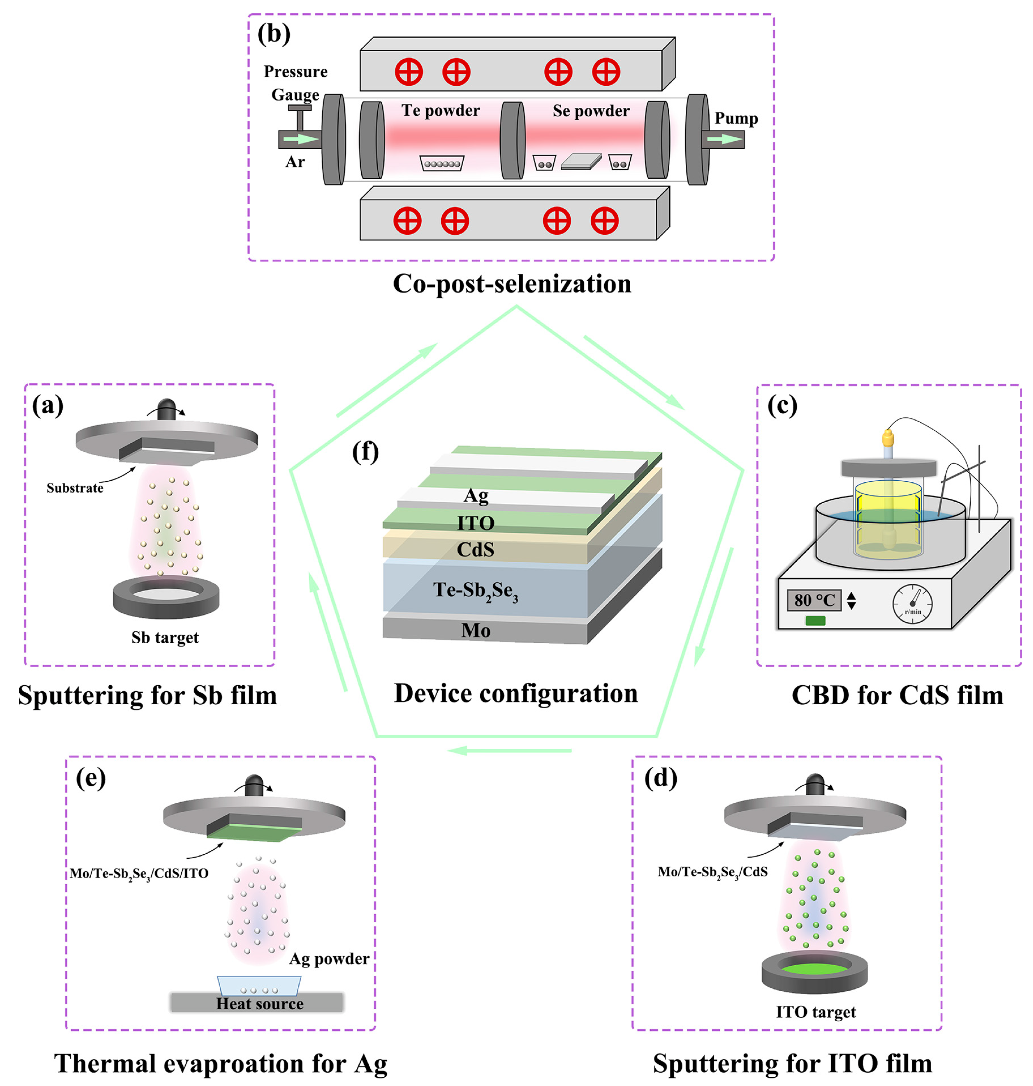
Firstly, a radiofrequency (RF) magnetron sputtering deposition method was used to obtain the Sb metallic precursors thin films. Before the depositions, Mo-coated glass substrates were ultrasonically cleaned with detergent solution, deionized water, and ethanol for 20 min, respectively. Before beginning to deposit the Sb thin film, the background pressure of the sputtering system was reduced to 8.0 × 10⁻⁴ Pa. At a flow rate of 35 sccm high-purity (>99.999%) Ar gas was fed into the sputtering chamber. (Figure 1a) During the sputtering process, the power and duration were fixed at 30 W and 45 min, respectively. The working pressure was kept at 1.8 Pa. To obtain the Te-Sb2Se3 thin film, The precursor thin films were subsequently put into a vacuum tubular furnace for post-selenization treatment (Figure 1b). The selenization temperature and the quantity of Te powder were adjusted from 440 °C to 480 °C and from 0 g to 0.2 g, respectively, to study the influence of selenization parameters on device behavior. A total of 0.4 g of selenium powder was applied to each sample for the selenizaiton process. The temperature of the selenium source and tellurium source is controlled by two temperature zones. Before the selenization the tubular furnace was evacuated to a low background pressure. After that, the furnace was filled with high purity Ar (>99.999%), and the working pressure was maintained at 7 × 10⁴ Pa throughout the annealing process. Thereafter, at a rate of 20 °C/min, the furnace temperature was increased to 440 °C for the Te source and 420 °C for the Se source, respectively. For each sample, the selenizing time was set at 15 min. After the heating cycle was over, the furnace automatically cooled to room temperature.

Figure 1.
Schematic diagram of the preparation process of the Sb2Se3 solar cell. (a) sputtering for Sb thin film. (b) Co-post-selenization heat treatment of Te-doped Sb2Se3. (c) Chemical bath deposition (CBD) method deposited CdS buffer layer. (d) A magnetron sputter-deposited ITO window layer. (e) Thermal evaporation for Ag electrode. (f) The schematic layout of the completed Te-doped Sb2Se3 device.
2.2. Te-Sb2Se3 Thin-Film Solar Cell Preparation
Chemical bath deposition (CBD) was used to obtain the cadmium sulfide (CdS) buffer layer following the post-selenization procedure. (Figure 1c). The CdS layer was then coated with an indium tin oxide (ITO) layer using magnetron sputtering for 25 min at a DC voltage of 120 W (Figure 1d). The active device area was 0.12 cm2 after Ag conductors were thermally evaporated onto the ITO surface to create metallic contact. Figure 1f shows an overall schematic layout of the device preparation procedure and the device configuration.
2.3. Device Characterization
The scanning electron microscope (SEM, SUPRA 55, Zeiss, Jena, Germany) was introduced to characterize the Te-Sb2Se3 thin film morphology. The crystal orientation of the Te-Sb2Se3 films was examined using X-ray diffraction (XRD, Ultima-iv, Rigaku, Tokyo, Japan, CuK radiation under operation circumstances of 40 kV and 40 mA from 10° to 60°). The excitation frequency used to produce the Raman spectra (Renishaw, Wotton-under-Edge, UK) was 532. A class AAA solar simulator (SCS1011, Zolix, Beijing, China) was used to measure the current density-voltage (J-V) profiles of the devices under illumination of 100 mW cm2 AM 1.5 G light at room temperature. A Zolix SCS101 system and a Keithley 2400 source meter were used to quantify the external quantum efficiency (EQE) spectra. A parameter analyzer was used to conduct capacitance-voltage (C-V) and drive-level capacitance profiles (DLCP) tests (Keithley, 4200A-SCS, Cleveland, OH, USA). The admittance spectroscopy (AS) measurement was performed using a Victor digital LCR meter in the frequency band of 100–1 MHz and 180–330 K (Lake Shore, 325 cryogenic temperature controller, Carson, CA, USA). A CHI600E Electrochemical Workstation (Shanghai, China) (was used to perform the electrochemical impedance spectroscopy (EIS).
3. Results and Discussion
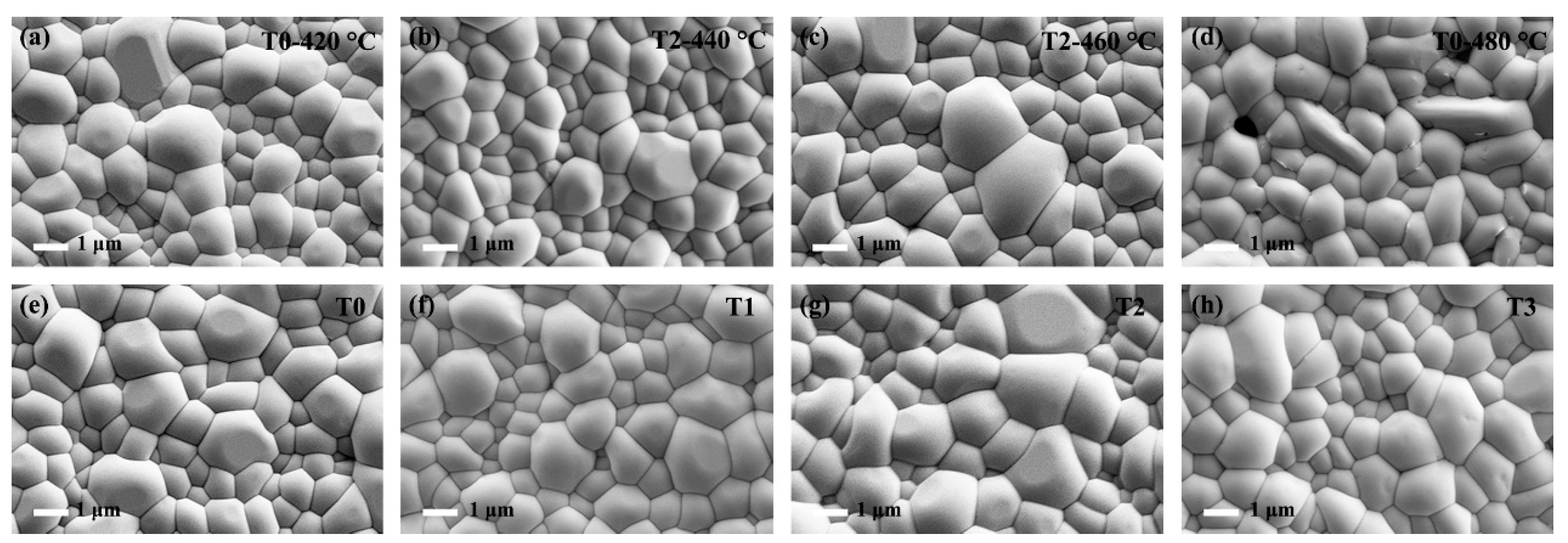
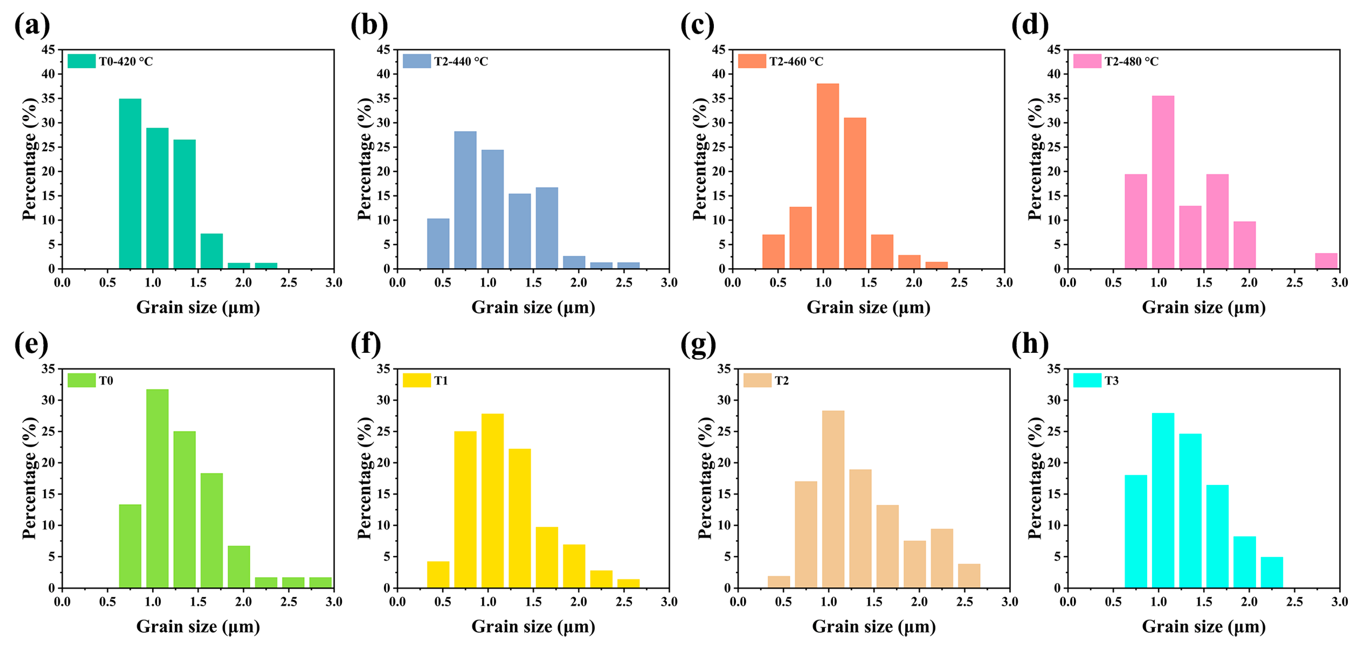
The Te-Sb2Se3 thin films selenized with the different weights of Te powder were denoted as T0, T1, T2, and T3, respectively. T0 corresponds to the weight of 0 g Te powder, T1 corresponds to the weight of 0.1 g Te powder, T2 corresponds to the weight of 0.15 g Te powder and T3 corresponds to the weight of 0.2 g Te powder. Besides, the Te-Sb2Se3 thin films selenized under different temperatures were denoted as T2-440 °C, T2-460 °C, and T2-480 °C, respectively, and the pristine Sb2Se3 thin film was denoted as T0-420 °C. Several carefully planned experiments were performed to gain insight into the connection between the Te source temperature and the thin film quality. Figure 2a–c depicted the SEM morphology of the pristine sample and the Te-doped sample under the same Se source temperature but with the various Te source temperature. As can be seen, the T0-420 °C, T2-440 °C, and T2-460 °C thin films showed a similar morphology. With the increased temperature of the Te source, the crystal grain size also presented an increasing trend. However, pinholes appeared on the surface of the T2-480 °C sample (Figure 2d). The film significantly deteriorated probably because the nucleation and crystal growth processes had changed, leading to the formation of apparent holes. The particle size distribution versus the fine frequency histograms were depicted in Figure 3. After Te doping, the T2-460 °C thin films revealed a steady improvement in compactness and uniformity as the temperature was raised from 440 to 460 °C, which was accompanied by a corresponding rise in average grain size from 1.02 m to 1.28 m. Nevertheless, when the temperature increased to 480 °C, some pinholes appeared. Under a high temperature, Se is simpler to evaporate out during the selenization process compared with Te, leading to the generation more pinholes. Subsequently, the Te and Se source temperatures were fixed at 460 °C and 420 °C, respectively. The surface SEM pictures of the Sb2Se3 thin films with various weights of Te powder during the selenization treatment are illustrated in Figure 2e–h. All the as-obtained films displayed a relatively dense surface morphology. As depicted in Figure 3e–f, the average grain size of the T0 sample is 1.3 μm. Once the Te with weight of 0.1 and 0.15 g were added during the selenization treatment, the average grain size increased to 1.31 and 1.36 μm, respectively. However, when the weight of Te increased to 0.2 g, the average grain size decreased to 1.20 μm. The grain growth in this instance was presumably prevented by more Te being concentrated at the grain boundaries.

Figure 2.
Surface morphology image of the pure Sb2Se3 and Te-Sb2Se3 thin films under different selenization temperatures, denoted as (a) T0-420 °C, (b) T2-440 °C, (c) T2-460 °C, and (d) T2-480 °C, respectively. Top-view SEM picture of the pristine Sb2Se3 and Te-Sb2Se3 thin films under the different weights of the Te source, labeled as (e) T0, (f) T1, (g) T2, and (h) T3, respectively.

Figure 3.
The particle size distribution versus the fine frequency histograms of the pristine Sb2Se3 and Te-Sb2Se3 thin films under different selenization temperatures are denoted as (a) T0-420 °C, (b) T2-440 °C, (c) T2-460 °C, and (d) T2-480 °C, respectively. (e–h) The particle size distribution versus the fine frequency histograms of the pristine Sb2Se3 and Te-Sb2Se3 thin films under the different weights of the Te source, labeled as (e) T0, (f) T1, (g) T2, and (h) T3, respectively.
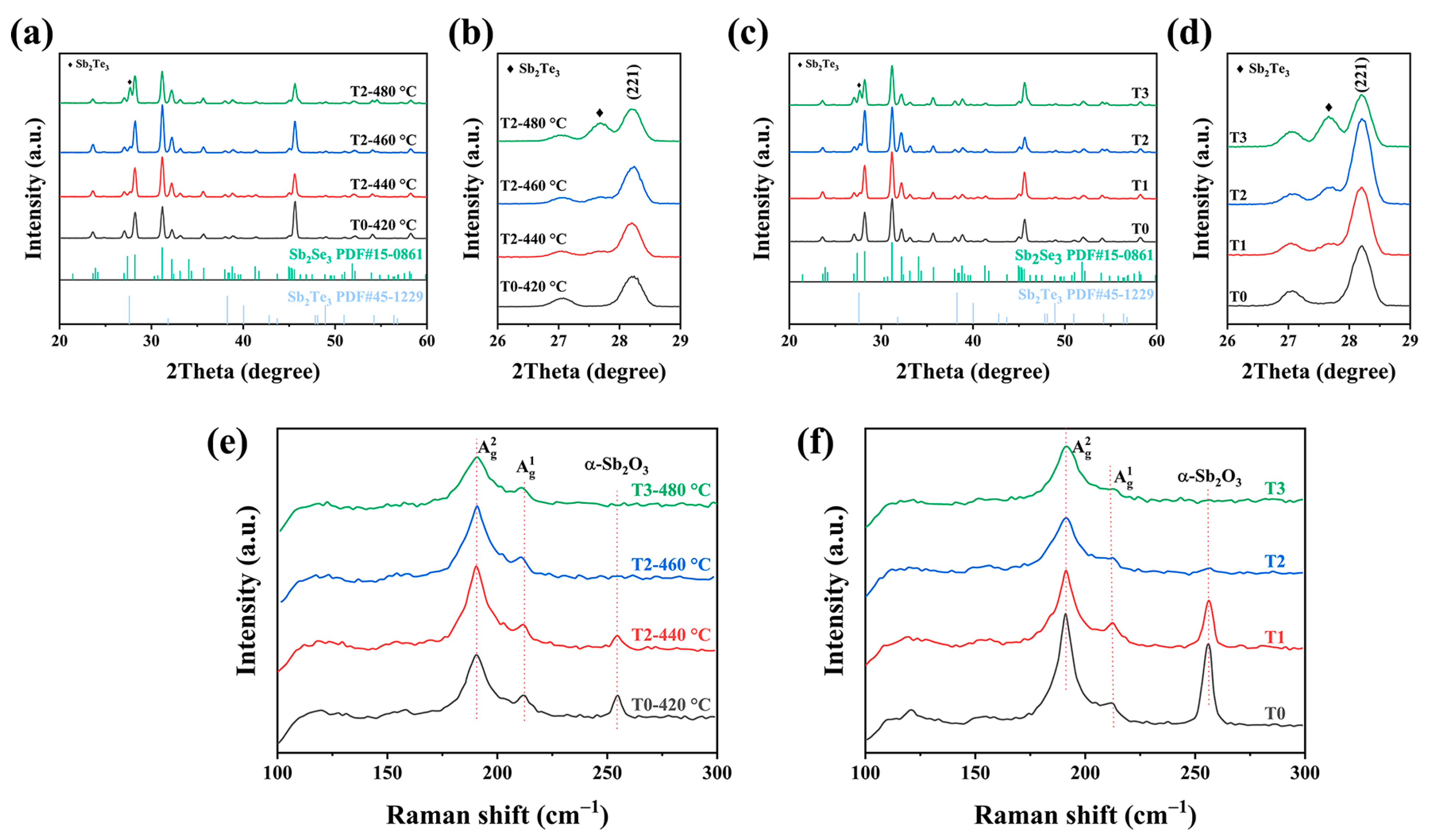
The introduction of the X-ray diffraction (XRD) characterization was conducted to confirm the crystal structure of the as-obtained thin films. Figure 4 displayed the XRD patterns of the pure sample and the Te-doped samples at various weights and temperatures. It is clear that all of the sample diffraction peaks matched the typical ortho-rhombic Sb2Se3 diffraction patterns well (JCPDS 15-0861). Figure 4b showed the detailed analysis of enlarged XRD patterns. There are additional diffraction peaks indexed in the Te-doped Sb2Se3 thin films, which was in good agreement with the Sb2Te3 patterns (JCPDS 45-1229). Once we introduced the Te source during the selenization process, an additional Sb2Te3 phase appeared, rather than the peak of Sb2Se3 shifting. Besides, when increasing the weight of Te, the XRD patterns exhibited the same peak position (Figure 4c). This observation proved that increasing the reaction temperature and weight does not lead to the Te atoms substituting for the Se atoms in the lattice. It means that under the competitive reaction between the Te and Se during the selenization process it tended to form Sb2Te3-doped Sb2Se3, instead of the alloy-type Sb2(Se,Te)3. Moreover, it is notable that the [221] and [211] diffraction peaks intensity increased before decreasing, no matter whether increasing the reaction temperature or increasing the weight of Te. However, if the temperature and the weight of Te were too high and/or too much, e.g., 480 °C and 0.2 g, there was a slight decrease in the intensity of the diffraction peak, which could be explained by the formation of the Sb2Te3 phase that prevented the grain growth. Figure 4e,f demonstrated the Raman images of the thin films under different temperatures and weights of Te. As depicted in the Raman spectra, There were two obvious peaks centered around 189 and 210 cm−1, which are frequently ascribed to the Sb-Se-Sb bending vibration of Sb2Se3 [16,17]. The stabilization of the orthorhombic phase has been further confirmed, which is in accordance with the XRD results. Except that, an additional peak that appeared at 253 cm−1 was more closely related to α-Sb2O3 [18]. After introducing Te during the selenization, the peak around 253 cm−1 disappeared, and the peak intensity for Te-doped Sb2Se3 thin film decreased with higher insertion. Moreover, the energy-dispersive X-ray spectroscopy (EDS) was introduced to measure the element composition of the absorber layers. Such a situation may be due to the mitigation of surface oxidation or the tunning of the (Se/Sb) ratio (Table 1 and Table 2). Interestingly, it can be shown that the Sb2O3 peak got reduced at 460 °C and completely disappeared at 480 °C. A similar trend can be noticed in Figure 4e with increasing the weight of the Te source, which indicated that a lower temperature and weight for the Te source are insufficient to occupy the Sb sites during the selenization process.
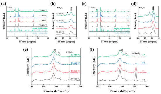
Figure 4.
(a) Virgin Sb2Se3 and Te-Sb2Se3 thin film XRD patterns at various selenization temperatures, and (b) enlarged region of the XRD patterns. (c) XRD patterns of the pristine Sb2Se3 and the Te-Sb2Se3 thin films at different weights of Te source, and (d) enlarged region of the XRD pattern. (e) Raman spectroscopy of the virgin Sb2Se3 and the Te-Sb2Se3 thin films under different selenization temperatures. (f) Raman spectroscopy of the virgin Sb2Se3 and the Te-Sb2Se3 thin films under different weights of the Te source.

Table 1.
Elemental composition of the Sb2Se3 thin films deposited at the different doping condition (temperature).

Table 2.
Elemental composition of the Sb2Se3 thin films deposited at the different doping condition (Te weight).
Overall, a suitable selenization temperature and doping weight were crucial for obtaining high-quality Sb2Se3 thin film via carefully optimized selenization parameters. On the one hand, the introduction of Te can effectively induce the [hk1] orientation of the Sb2Se3 thin films, leading to higher carrier transport and extraction. On the other hand, harmful surface oxidation can be effectively mitigated after Te inclusion. Ultimately, the temperature and weight of the Te source were set at 460 °C and 0.15 g, respectively, while the temperature of the Se source was set at 420 °C. These values were determined to be the optimal selenization parameters.
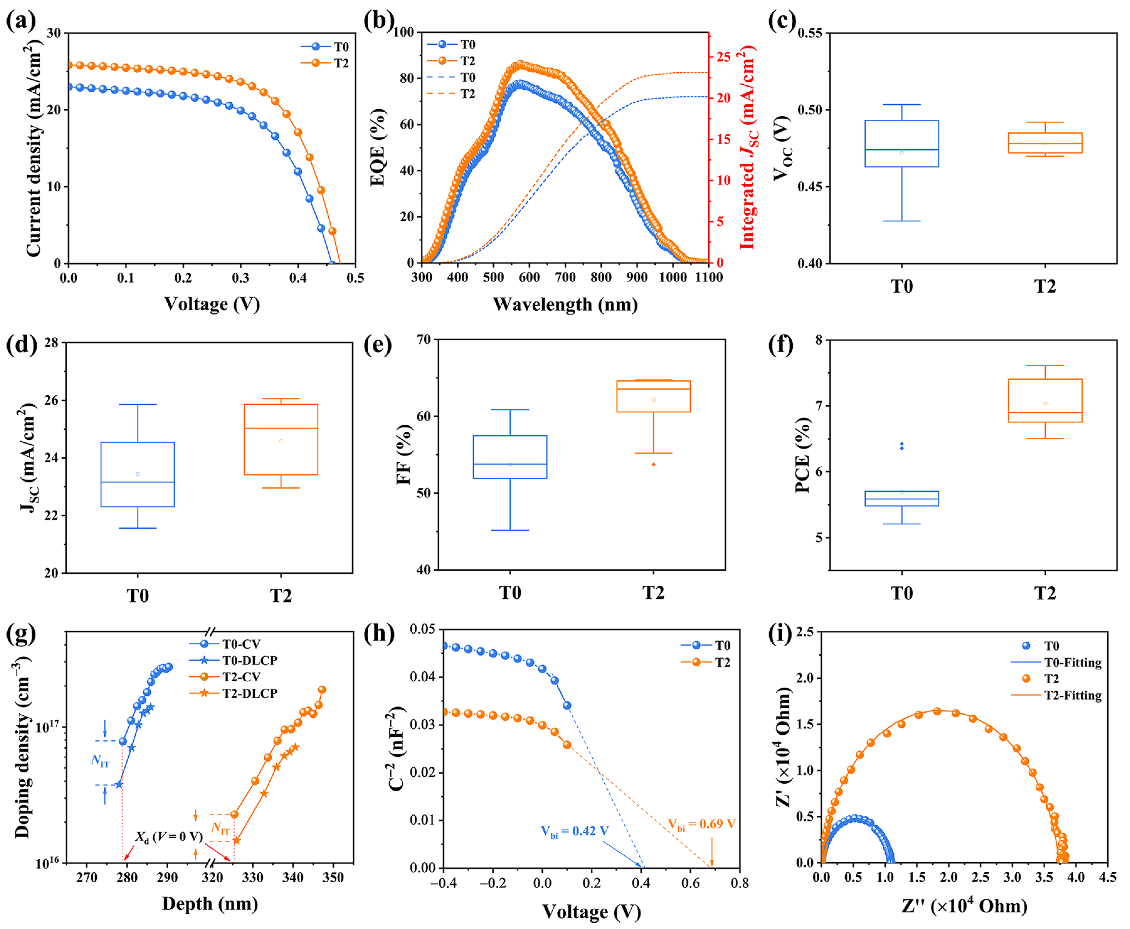
To investigate the photovoltaic properties of the Te-doped Sb2Se3 thin films, Mo/Te-Sb2Se3/CdS/ITO/Ag was used in the fabrication of the devices. The optimized films and pristine films were used for comparison. Moreover, for clarity of description, the two samples were denoted as T0 and T2, respectively. The current density-voltage (J-V) curves of the devices were characterized under simulated AM 1.5 sunlight, and Table 3 shows the detailed photovoltaic properties of the two devices. The pristine Sb2Se3 solar cell exhibited a PCE of 6.42% with a VOC of 460 mV, a JSC of 23.15 mA/cm2, and an FF of 60.86%. While after Te-doping, the T2 device exhibited a much superior performance with a PCE of 7.61%, along with a VOC of 474 mV, a JSC of 25.88 mA/cm2, and an FF of 64.09% (Figure 5a). Notably, the enhancement of the performance after Te-doping could be mainly due to the synergetic development of the photovoltaic parameters, confirming that Te-doping may enhance the efficiency of the carrier transport, leading to better thin films. Besides, Figure 5c–f depicted the statistics box diagrams of performance parameters from these two devices, demonstrating the excellent repeatability of device fabrication.

Table 3.
Device characteristics of the Sb2Se3 solar cells with or without Te doping.

Figure 5.
(a) The J-V curves, and (b) the EQE spectroscopy of the T0 and T2 devices. Statistical distribution of the photovoltaic parameter of the T0 and T2 devices, involving (c) VOC, (d) JSC, (e) FF, and (f) PCE. (g) CV and DLCP characterization of the T0 and T2 devices, and (h) Plots of C−2 against V. (i) Nyquist plot of the T0 and T2 devices.
To further analyze the photo responses of the devices, the external quantum efficiency (EQE) spectra of both devices was conducted, as displayed in Figure 5b. Compared with the virgin device, the T2 device exhibited a much higher response in the wavelength region from 500 nm to 900 nm, which is not only corresponding to better carrier transport and extraction leading to a higher JSC but also suggests fewer recombination losses within both the bulk and the interface. The integrated JSC values of the devices were 20.17 and 23.13 mA/cm2, respectively, which are consistent with the values obtained from the J-V curves.
Capacitance-voltage (C-V) and deep-level capacitance profiling (DLCP) tests were performed to assess the defect density of the Sb2Se3 absorber layers more clearly and the combination properties of the solar cells. Figure 5g presented the pattern produced by C-V and DLCP. Information on interface defects could be directly obtained from the differences in doping density between the CV and DLCP data. The plots of NCV and NDLCP against the depth x can be calculated based on the following equation [19]:
where C0 and C1 are two quadratic fitting parameters generated from the DLCP data; εr,n and εr,p are the relative permittivity of CdS and Sb2Se3, respectively; A is the device area and; ND is the doping density of CdS. The interface defect density of the T0 device was 4.05 × 1016 cm−3, while after Te-doping, the interface defect density decreased to 8.45 × 1015 cm−3, indicating that there were fewer surface defects in Te-doped Sb2Se3 absorber. It is noteworthy that the carriers could be difficult to capture as a recombination center, but more easy to transport at the interface with the decreasing interface defect density, leading to much superior device performance [20]. In addition, the depletion width of the T2 device (325 nm) is obviously larger than that of the T0 device (278 nm). The collection and extraction of the charge carrier benefit from the wider depletion width [21]. As revealed in Figure 5h, the built-in voltage (Vbi) of the T0 device is 0.42 V, and it increased to 0.69 V for the T2 device. The introduction of the Te enlarged the Vbi of the device forming an enhanced built-in voltages, supporting the improvement of the VOC [22]. We used electrochemical impedance spectroscopy (EIS) measurements at frequencies ranging from 1 Hz to 1 MHz to shed light on the carrier recombination mechanism. The Nyquist curves were depicted in Figure 5i, and the inset graph demonstrates the corresponding fitted curves using an equivalent electrical circuit. Where Rs represents internal resistance, and Rrec represents recombination resistance [23,24]. Strikingly, the Rrec increases from 10.9 kΩ to 37.3 kΩ after the introduction of Te-doping, implying that the severe carrier accumulation and recombination at the interface have been effectively passivated, thus providing a higher photovoltaic performance [25].
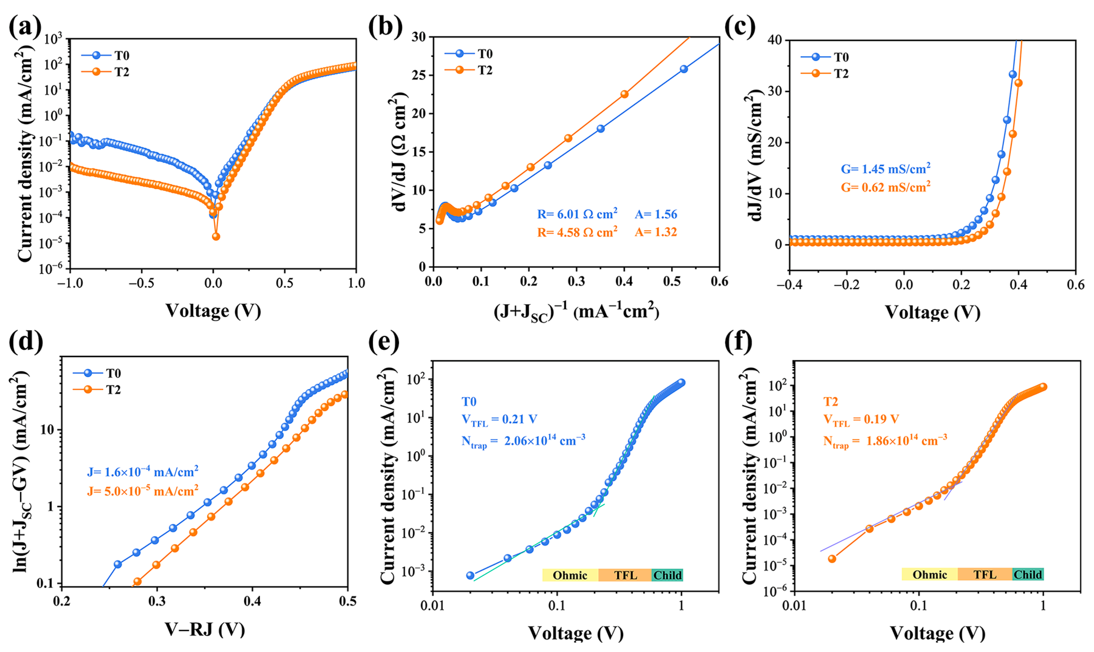
The dark J-V characterization was conducted to scrutinize the intrinsic electrical behaviors of the devices, as illustrated in Figure 6. A single exponential diode equation can be utilized to fit the shunt conductance (G), series resistance (RS), diode ideality factor (A), and reverse saturation current density (J0) [26,27].

Figure 6.
Electrical characteristics of the T0 and T2 devices include the following: (a) dark J-V curves; (b) series resistance R and ideality factor A; (c) shunt conductance G; and (d) reverse saturation current density J0. (e,f) The corresponding logarithmic J-V curves of the T0 and T2 devices.
Compared with the two devices, a lower reverse current density is found in the T2 device, suggesting that fewer carriers were trapped by defect recombination centers and more carriers successfully swept out of the device. As demonstrated in Figure 6b, the R-value is determined to be 6.08 and 4.58 Ω cm2 for T0 and T2 devices, respectively, and the obtained values of A were 1.56 and 1.32, respectively. The smaller value of A implies that the space-charge region (SCR) recombination has been suppressed effectively. Additionally, it is discovered that the J0 value of the T2 device is 5.0 × 10⁻⁵ mA/cm2, which is lower than that of the T0 device (1.6 × 10⁻⁵ mA/cm2). After Te-doping, the optimized absorber possesses a better quality, as well as a better PN junction quality, leading to a higher PCE. Finally, to better understand the thin films defect states, we introduced the standard space charge limited current (SCLC) model. Figure 6e,f illustrated the logarithmic J-V curves, which can be sectioned into three regimes: the ohmic region at low voltages (exponent n = 1), the trap-filled limit (TFL) region at intermediate voltages (n > 3), and the trap free child region at high voltages (n > 2). When the bias voltage exceeds the kink point, which corresponds to the trap-filled limit voltage, the injected carrier fills the trap states in the TFL region (VTFL). [28] Then the defect density of the Sb2Se3 thin film can be determined using the VTFL value according to the following equation [5]:
where L represents the thickness of the Sb2Se3 thin film, q represents the elementary charge, εr represents the permittivity of the Sb2Se3 and ε0 represents the vacuum permittivity. The defect densities were calculated to 2.06 × 1014 cm−3 and 1.86 × 1014 cm−3, respectively. The SCLC characterization confirmed that the Sb2Se3 films with larger grain sizes and benign orientation are capable of reducing the inter-defect density, echoing the previous analysis.
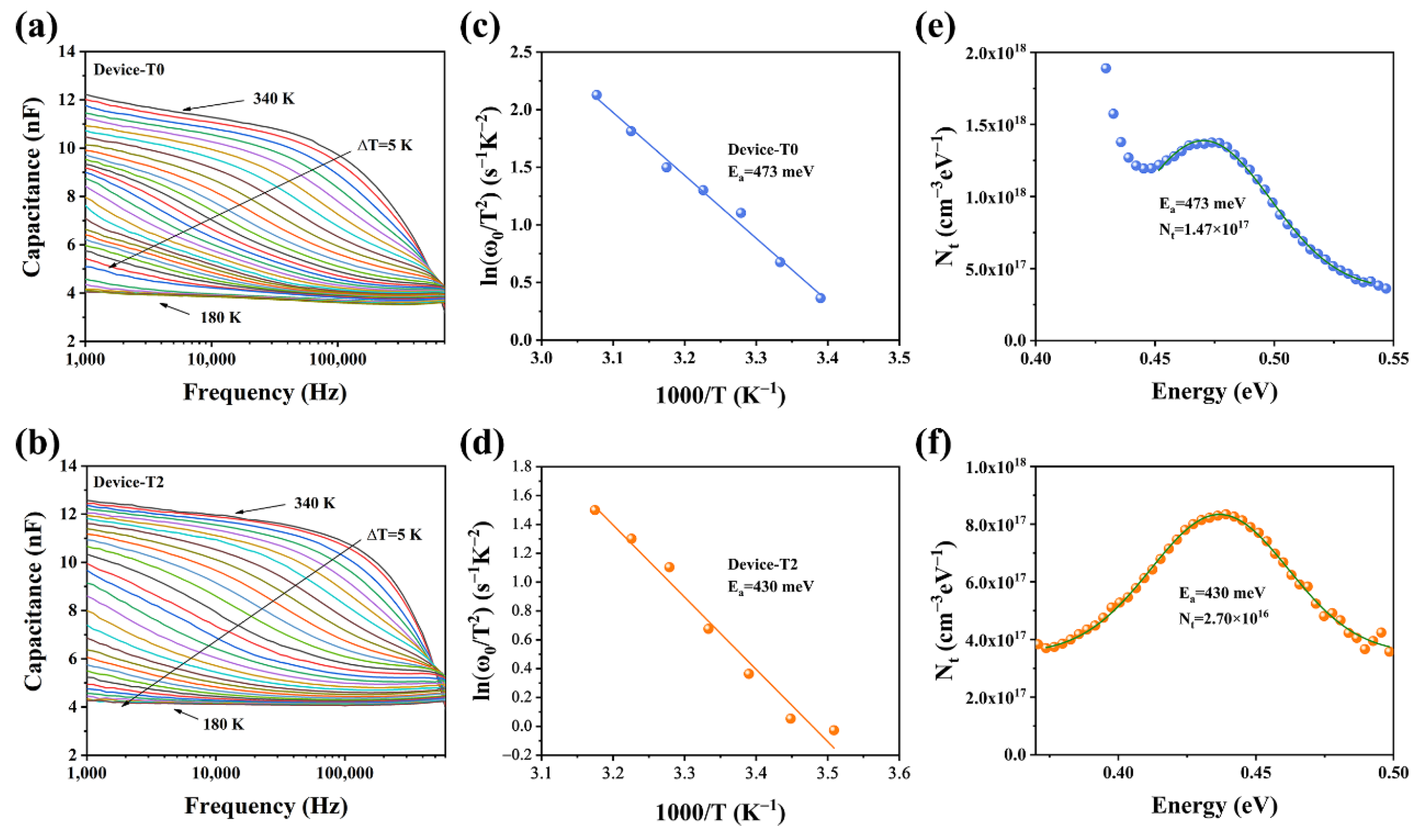
To further determine the defect characters of the Sb2Se3 films, the admittance spectroscopy (AS) measurements were applied. Figure 7a,b demonstrated the capacitance–frequency (C–f) curves for the temperature range of 180–340 K at 10 K intervals. The capacitance at low frequency indicates the response of the sum of the free carrier and deep defect, while the capacitance at high frequency represents the response of the free carrier density, according to the Kimerling model [29,30]. Compared to the T0 device, the capacitance of the T2 device showed less change as a function of frequency. Te-doping may be able to successfully passivate defects to improve the quality of the absorber layer because the more significant the frequency dependency of the capacitance, the greater the defect densities in the absorber. The angular frequency point at the maximum of the ωdC/dω plot was used to calculate the Arrhenius plots for the inflection points in the two AS results, which are exhibited in Figure 7c,d. Then, using the following equation, we determined the defect activation energies (Ea) based on the slopes of the Arrhenius plots [31,32].
where Ea is the defect electronic state level and the ω0 is the step frequency, υ0 is the pre-exponential factor. The Ea values of 473 and 430 meV are determined for T0 and T2 devices, respectively, indicating that they are of the same type of defect. Based on a previous report, the Sb2Se3 thin films deposited via a post-selenization are slightly Se-rich. Under Se-rich conditions, the dominant defects of the Sb2Se3 thin films are antimony vacancy (VSb) and selenium antisite (SeSb) defects [33]. As a function of frequency, only one capacitance step can be recognized. It is difficult to differentiate them from each other. Thus, we tentatively considered both these defects (VSb and SeSb) to be the dominant defects in our devices. It is well known that defects with higher Ea values are more likely to become recombination centers, which lowers device performance. The defect densities of the two devices were fitted with a Gaussian curve employing following equation to provide relative quantitative data about the defect [34,35].
where Vd represents the built-in voltage of the P-N junction, E represents the energetic gap between the defect energy level and the CBM or VBM, and Nt represents the defect density. Figure 7e,f depicted the defect density of the T2 device (2.70 × 1016 cm−3), which was considerably less than that of the T0 device (1.47 × 1017 cm−3). In this regard, Te doping was essential in passivating the Sb2Se3 bulk defects.
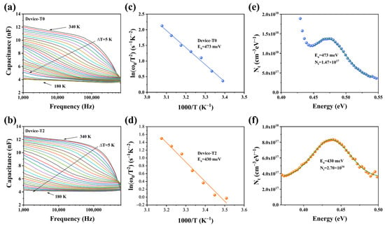
Figure 7.
(a,b) Capacitance−frequency−temperature (C−f−T) spectra (different colored lines represent capacitance values at different temperatures) of the T0 and T2 devices, respectively; (c,d) Arrhenius plots of the T0 and T2 devices; and (e,f) defect densities of T0 and T2 devices, respectively.
4. Conclusions
In conclusion, our work has investigated the impact of Te doping on the functionality of the device. A two-step deposition process (sputtering and post-selenization) was introduced to prepare high-quality Te-Sb2Se3. The introduction of Te in the selenization process tended to form Sb2Te3-doped Sb2Se3, instead of the alloy-type Sb2(Se,Te)3, due to the competitive reaction between Te and Se. By a fine-tuning of the selenization parameters, high-quality, large grain size, and benign orientation Te-Sb2Se3 thin films can be successfully fulfilled. The characterizations and analyses have demonstrated that Te doping in Sb2Se3 not only enhances the quality of the Sb2Se3 absorber, leading to mitigation of surface oxidation, but also induces the thin film to present a favorable [hk1] orientation, leading to a better carrier transport. Finally, the champion Te-doped Sb2Se3 device exhibited a PCE of 7.61% with a VOC of 474 mV, a JSC of 25.88 mA/cm2, and an FF of 64.09%. This study demonstrated an effective doping strategy, which can significantly enhance the Sb2Se3 physical properties, providing a helpful direction for the creation of Sb2Se3 solar cells.
Author Contributions
Conceptualization, S.C. and G.L.; methodology, G.C., M.A. Z.S. and R.T.; validation, P.F.; formal analysis, S.C. and C.F.; investigation, G.C. and X.L.; resources, R.T.; writing—original draft preparation, G.C.; writing—review and editing, S.C., C.F. and G.L.; visualization, P.F.; supervision, S.C. and G.L.; funding acquisition, S.C, C.F. and G.L. All authors have read and agreed to the published version of the manuscript.
Funding
This work was supported by National Natural Science Foundation of China (No. 62104156, 62104157, 62074102), Guangdong Basic and Applied Basic Research Foundation (2022A1515010979, 2023A1515011256) China, Science and Technology plan project of Shenzhen (SGDX20190919102801693, 20220808165025003, 20200812000347001) China.
Data Availability Statement
The data presented in this study are available on request from the corresponding authors.
Conflicts of Interest
The authors declare no conflict of interest.
References
- Tang, R.; Chen, S.; Zheng, Z.; Su, Z.; Luo, J.; Fan, P.; Zhang, X.; Tang, J.; Liang, G. Heterojunction Annealing Enabling Record Open-Circuit Voltage in Antimony Triselenide Solar Cells. Adv. Mater. 2022, 34, 2109078. [Google Scholar] [CrossRef] [PubMed]
- Chen, S.; Fu, Y.; Ishaq, M.; Li, C.; Ren, D.; Su, Z.; Qiao, X.; Fan, P.; Liang, G.; Tang, J. Carrier recombination suppression and transport enhancement enable high-performance self-powered broadband Sb2Se3 photodetectors. Infomat 2023, e12400. [Google Scholar] [CrossRef]
- Liu, C.; Wu, S.; Gao, Y.; Feng, Y.; Wang, X.; Xie, Y.; Zheng, J.; Zhu, H.; Li, Z.; Schropp, R.E.; et al. Band Gap and Defect Engineering for High-Performance Cadmium-free Sb2(S,Se)3 Solar Cells and Modules. Adv. Funct. Mater. 2022, 32, 2209601. [Google Scholar] [CrossRef]
- Lin, J.; Chen, G.; Ahmad, N.; Ishaq, M.; Chen, S.; Su, Z.; Fan, P.; Zhang, X.; Zhang, Y.; Liang, G. Back contact interfacial modification mechanism in highly-efficient antimony selenide thin-film solar cells. J. Energy Chem. 2023, 80, 256–264. [Google Scholar] [CrossRef]
- Luo, Y.; Chen, G.; Chen, S.; Ahmad, N.; Azam, M.; Zheng, Z.; Su, Z.; Cathelinaud, M.; Ma, H.; Chen, Z.; et al. Carrier Transport Enhancement Mechanism in Highly Efficient Antimony Selenide Thin-Film Solar Cell. Adv. Funct. Mater. 2023, 2213941. [Google Scholar] [CrossRef]
- Liang, G.; Chen, M.; Ishaq, M.; Li, X.; Tang, R.; Zheng, Z.; Su, Z.; Fan, P.; Zhang, X.; Chen, S. Crystal Growth Promotion and Defects Healing Enable Minimum Open-Circuit Voltage Deficit in Antimony Selenide Solar Cells. Adv. Sci. 2022, 9, 2105142. [Google Scholar] [CrossRef]
- Fan, P.; Chen, G.-J.; Chen, S.; Zheng, Z.-H.; Azam, M.; Ahmad, N.; Su, Z.-H.; Liang, G.-X.; Zhang, X.-H.; Chen, Z.-G. Quasi-Vertically Oriented Sb2Se3 Thin-Film Solar Cells with Open-Circuit Voltage Exceeding 500 mV Prepared via Close-Space Sublimation and Selenization. ACS Appl. Mater. Interfaces 2021, 13, 46671–46680. [Google Scholar] [CrossRef]
- Chen, S.; Liu, T.; Zheng, Z.; Ishaq, M.; Liang, G.; Fan, P.; Chen, T.; Tang, J. Recent progress and perspectives on Sb2Se3-based photocathodes for solar hydrogen production via photoelectrochemical water splitting. J. Energy Chem. 2022, 67, 508–523. [Google Scholar] [CrossRef]
- Zhao, Y.; Wang, S.; Jiang, C.; Li, C.; Xiao, P.; Tang, R.; Gong, J.; Chen, G.; Chen, T.; Li, J.; et al. Regulating Energy Band Alignment via Alkaline Metal Fluoride Assisted Solution Post-Treatment Enabling Sb2(S,Se)3 Solar Cells with 10.7% Efficiency. Adv. Energy Mater. 2022, 12, 2103015. [Google Scholar] [CrossRef]
- Li, Y.; Zhou, Y.; Zhu, Y.; Chen, C.; Luo, J.; Ma, J.; Yang, B.; Wang, X.; Xia, Z.; Tang, J. Characterization of Mg and Fe doped Sb2Se3 thin films for photovoltaic application. Appl. Phys. Lett. 2016, 109, 232104. [Google Scholar] [CrossRef]
- Chen, S.; Qiao, X.; Zheng, Z.; Cathelinaud, M.; Ma, H.; Fan, X.; Zhang, X. Enhanced electrical conductivity and photoconductive properties of Sn-doped Sb2Se3 crystals. J. Mater. Chem. C 2018, 6, 6465–6470. [Google Scholar] [CrossRef]
- Tang, R.; Wang, X.; Jiang, C.; Li, S.; Liu, W.; Ju, H.; Yang, S.; Zhu, C.-F.; Chen, T. n-Type Doping of Sb2S3 Light-Harvesting Films Enabling High-Efficiency Planar Heterojunction Solar Cells. ACS Appl. Mater. Interfaces 2018, 10, 30314–30321. [Google Scholar] [CrossRef] [PubMed]
- Ma, Y.; Tang, B.; Lian, W.; Wu, C.; Wang, X.; Ju, H.; Zhu, C.; Fan, F.; Chen, T. Efficient defect passivation of Sb2Se3 film by tellurium doping for high performance solar cells. J. Mater. Chem. A 2020, 8, 6510–6516. [Google Scholar] [CrossRef]
- Rahman, R.S.; Asokan, K.; Zulfequar, M. Mitigation of Surface Oxidation in Sb2Se3 Thin Films Via Te Doping: An Effective Strategy towards Realization of Efficient Electronic Devices. J. Mater. Chem. C 2022, 126, 6065–6074. [Google Scholar] [CrossRef]
- Ren, D.; Luo, X.; Chen, S.; Zheng, Z.; Cathelinaud, M.; Liang, G.; Ma, H.; Qiao, X.; Fan, X.; Zhang, X. Structure, Morphology, and Photoelectric Performances of Te-Sb2Se3 Thin Film Prepared via Magnetron Sputtering. Nanomaterials 2020, 10, 1358. [Google Scholar] [CrossRef]
- Liang, G.-X.; Luo, Y.-D.; Chen, S.; Tang, R.; Zheng, Z.-H.; Li, X.-J.; Liu, X.-S.; Liu, Y.-K.; Li, Y.-F.; Chen, X.-Y.; et al. Sputtered and selenized Sb2Se3 thin-film solar cells with open-circuit voltage exceeding 500 mV. Nano Energy 2020, 73, 104806. [Google Scholar] [CrossRef]
- Li, Z.; Liang, X.; Li, G.; Liu, H.; Zhang, H.; Guo, J.; Chen, J.; Shen, K.; San, X.; Yu, W.; et al. 9.2%-efficient core-shell structured antimony selenide nanorod array solar cells. Nat. Commun. 2019, 10, 125. [Google Scholar] [CrossRef]
- Wang, C.; Lu, S.; Li, S.; Wang, S.; Lin, X.; Zhang, J.; Kondrotas, R.; Li, K.; Chen, C.; Tang, J. Efficiency improvement of flexible Sb2Se3 solar cells with non-toxic buffer layer via interface engineering. Nano Energy 2020, 71, 104577. [Google Scholar] [CrossRef]
- Luo, Y.-D.; Tang, R.; Chen, S.; Hu, J.-G.; Liu, Y.-K.; Li, Y.-F.; Liu, X.-S.; Zheng, Z.-H.; Su, Z.-H.; Ma, X.-F.; et al. An effective combination reaction involved with sputtered and selenized Sb precursors for efficient Sb2Se3 thin film solar cells. Chem. Eng. J. 2020, 393, 124599. [Google Scholar] [CrossRef]
- Tang, R.; Zheng, Z.-H.; Su, Z.-H.; Li, X.-J.; Wei, Y.-D.; Zhang, X.-H.; Fu, Y.-Q.; Luo, J.-T.; Fan, P.; Liang, G.-X. Highly efficient and stable planar heterojunction solar cell based on sputtered and post-selenized Sb2Se3 thin film. Nano Energy 2019, 64, 103929. [Google Scholar] [CrossRef]
- Chen, G.-J.; Tang, R.; Chen, S.; Zheng, Z.-H.; Su, Z.-H.; Ma, H.-L.; Zhang, X.-H.; Fan, P.; Liang, G.-X. Crystal Growth Promotion and Defect Passivation by Hydrothermal and Selenized Deposition for Substrate-Structured Antimony Selenosulfide Solar Cells. ACS Appl. Mater. Interfaces 2022, 14, 31986–31997. [Google Scholar] [CrossRef]
- Li, H.; Lin, L.; Yao, L.; Wu, F.; Wei, D.; Liu, G.; Huang, Z.; Chen, S.; Li, J.; Chen, G. High-Efficiency Sb2(S,Se)3 Solar Cells with New Hole Transport Layer-Free Back Architecture via 2D Titanium-Carbide Mxene. Adv. Funct. Mater. 2022, 32, 2110335. [Google Scholar] [CrossRef]
- Jiang, C.; Zhou, J.; Tang, R.; Lian, W.; Wang, X.; Lei, X.; Zeng, H.; Zhu, C.; Tang, W.; Chen, T. 9.7%-efficient Sb2(S,Se)3 solar cells with a dithieno[3,2-b:2′,3′-d]pyrrole-cored hole transporting material. Energy Environ. Sci. 2021, 14, 359–364. [Google Scholar] [CrossRef]
- Wang, S.; Zhao, Y.; Yao, L.; Li, C.; Gong, J.; Chen, G.; Li, J.; Xiao, X. Efficient and stable all-inorganic Sb2(S,Se)3 solar cells via manipulating energy levels in MnS hole transporting layers. Sci. Bull. 2021, 67, 263–269. [Google Scholar] [CrossRef]
- Wang, K.; Cheng, J.; Yang, X.; Hu, R.; Fu, L.; Huang, J.; Yu, J.; Li, L. Enhanced Photovoltaic Properties in Sb2S3 Planar Heterojunction Solar Cell with a Fast Selenylation Approach. Nanoscale Res. Lett. 2018, 13, 270. [Google Scholar] [CrossRef]
- Chen, S.; Ishaq, M.; Xiong, W.; Shah, U.A.; Farooq, U.; Luo, J.; Zheng, Z.; Su, Z.; Fan, P.; Zhang, X.; et al. Improved Open-Circuit Voltage of Sb2Se3 Thin-Film Solar Cells Via Interfacial Sulfur Diffusion-Induced Gradient Bandgap Engineering. Sol. RRL 2021, 5, 2100419. [Google Scholar] [CrossRef]
- Ishaq, M.; Deng, H.; Yuan, S.; Zhang, H.; Khan, J.; Farooq, U.; Song, H.; Tang, J. Efficient Double Buffer Layer Sb2(SexS1-x)3 Thin Film Solar Cell Via Single Source Evaporation. Sol. RRL 2018, 2, 1800144. [Google Scholar] [CrossRef]
- Guo, C.; Liang, X.; Liu, T.; Liu, Y.; Yang, L.; Lai, W.; Schropp, R.E.I.; Song, D.; Mai, Y.; Li, Z. 1D/3D Alloying Induced Phase Transition in Light Absorbers for Highly Efficient Sb2Se3 Solar Cells. Sol. RRL 2020, 4, 2000054. [Google Scholar] [CrossRef]
- Jasenek, A.; Rau, U.; Nadenau, V.; Schock, H.W. Electronic properties of CuGaSe2-based heterojunction solar cells. Part II. Defect spectroscopy. J. Appl. Phys. 2000, 87, 594–602. [Google Scholar] [CrossRef]
- Hu, X.; Tao, J.; Weng, G.; Jiang, J.; Chen, S.; Zhu, Z.; Chu, J. Investigation of electrically-active defects in Sb2Se3 thin-film solar cells with up to 5.91% efficiency via admittance spectroscopy. Sol. Energy Mater. Sol. Cells 2018, 186, 324–329. [Google Scholar] [CrossRef]
- Hu, X.; Tao, J.; Wang, Y.; Xue, J.; Weng, G.; Zhang, C.; Chen, S.; Zhu, Z.; Chu, J. 5.91%-efficient Sb2Se3 solar cells with a radio-frequency magnetron-sputtered CdS buffer layer. Appl. Mater. Today 2019, 16, 367–374. [Google Scholar] [CrossRef]
- Eisenbarth, T.; Unold, T.; Caballero, R.; Kaufmann, C.A.; Schock, H.-W. Interpretation of admittance, capacitance-voltage, and current-voltage signatures in Cu(In,Ga)Se2 thin film solar cells. J. Appl. Phys. 2010, 107, 034509. [Google Scholar] [CrossRef]
- Lian, W.; Cao, R.; Li, G.; Cai, H.; Cai, Z.; Tang, R.; Zhu, C.; Yang, S.; Chen, T. Distinctive Deep-Level Defects in Non-Stoichiometric Sb2Se3 Photovoltaic Materials. Adv. Sci. 2022, 9, 2105268. [Google Scholar] [CrossRef] [PubMed]
- Pan, Y.; Hu, X.; Guo, Y.; Pan, X.; Zhao, F.; Weng, G.; Tao, J.; Zhao, C.; Jiang, J.; Chen, S.; et al. Vapor Transport Deposition of Highly Efficient Sb2(S,Se)3 Solar Cells via Controllable Orientation Growth. Adv. Funct. Mater. 2021, 31, 2101476. [Google Scholar] [CrossRef]
- Walter, T.; Herberholz, R.; Müller, C.; Schock, H.W. Determination of defect distributions from admittance measurements and application to Cu(In,Ga)Se2based heterojunctions. J. Appl. Phys. 1996, 80, 4411–4420. [Google Scholar] [CrossRef]
Disclaimer/Publisher’s Note: The statements, opinions and data contained in all publications are solely those of the individual author(s) and contributor(s) and not of MDPI and/or the editor(s). MDPI and/or the editor(s) disclaim responsibility for any injury to people or property resulting from any ideas, methods, instructions or products referred to in the content. |
© 2023 by the authors. Licensee MDPI, Basel, Switzerland. This article is an open access article distributed under the terms and conditions of the Creative Commons Attribution (CC BY) license (https://creativecommons.org/licenses/by/4.0/).

