
Signatures of Electric Field and Layer Separation Effects on the Spin-Valley Physics of MoSe2/WSe2 Heterobilayers: From Energy Bands to Dipolar Excitons


Abstract
:1. Introduction
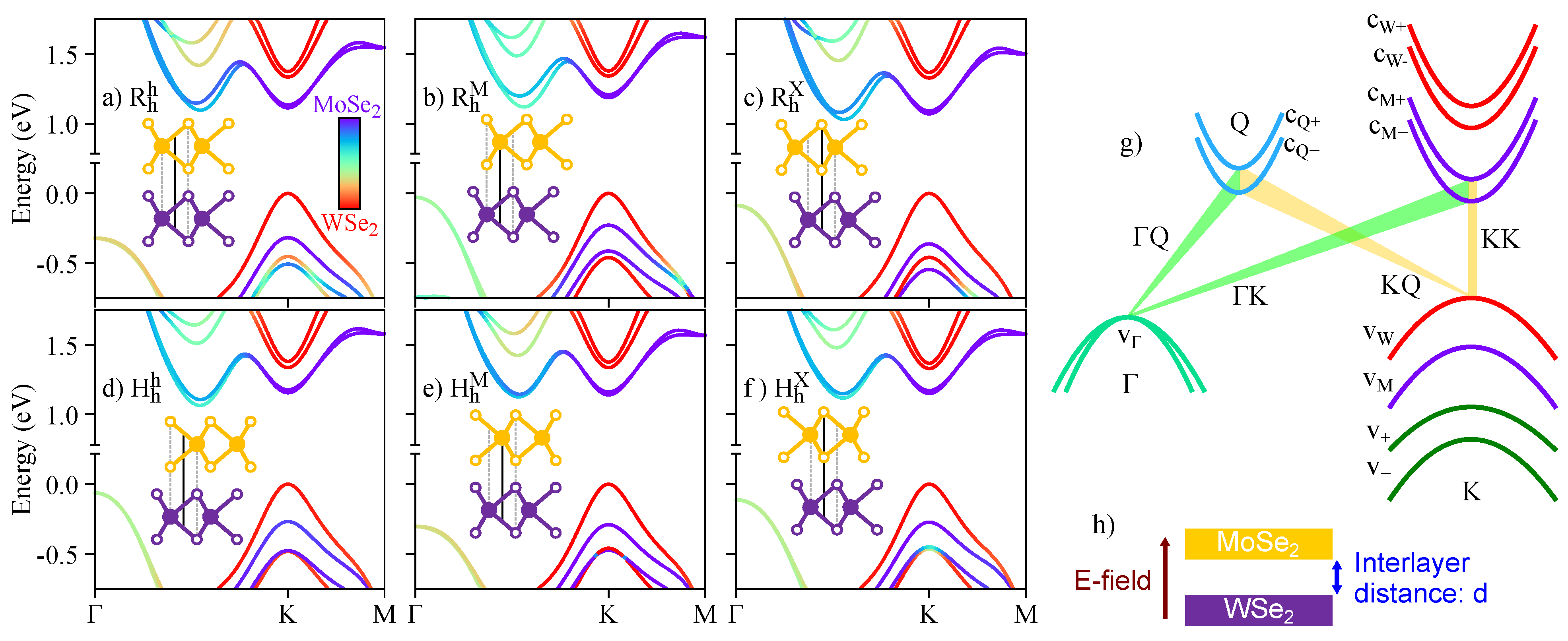
2. General Features of MoSe/WSe High-Symmetry Stackings
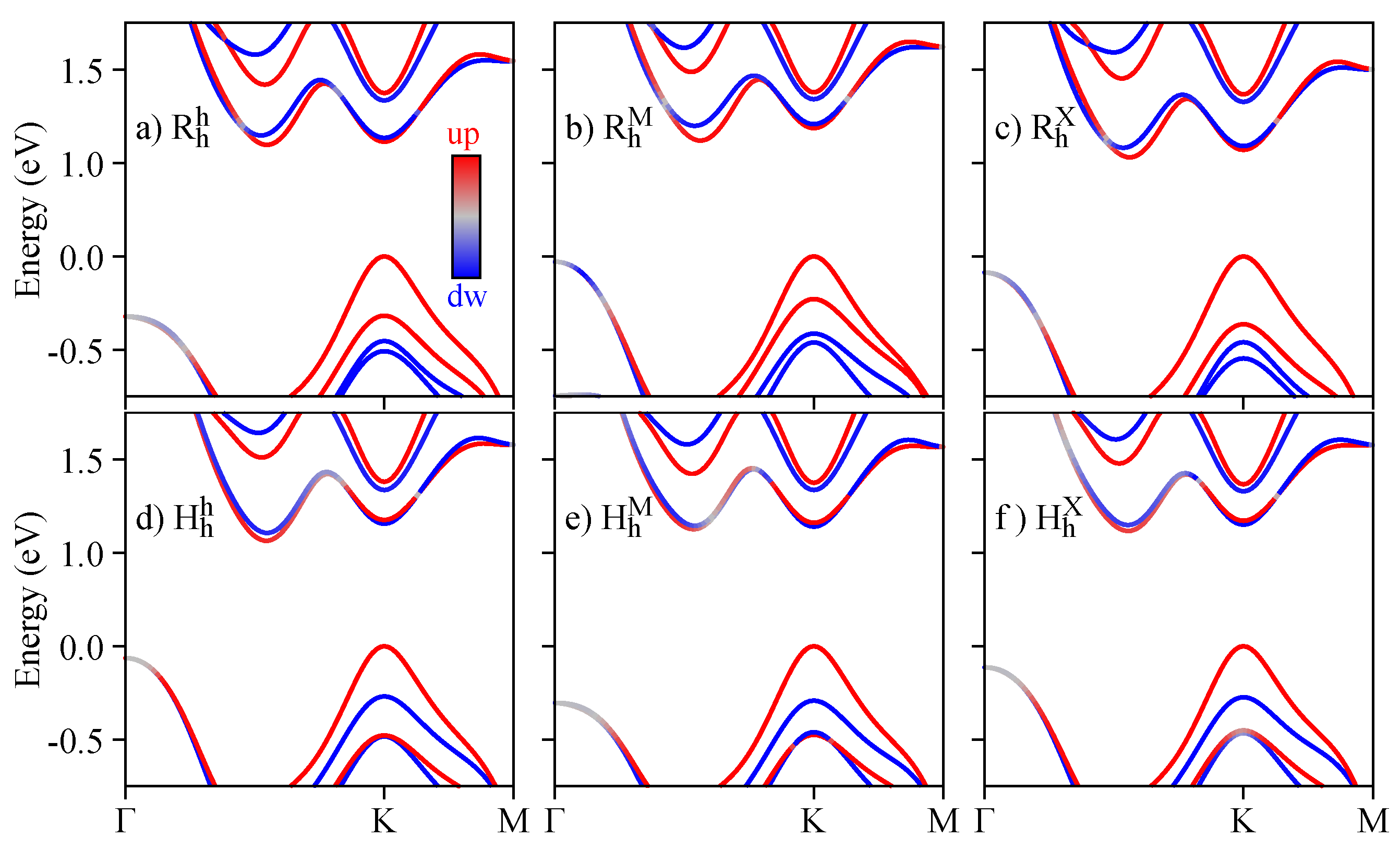
3. Spin-Valley Physics at the Band Edges
3.1. Pristine Heterostructures
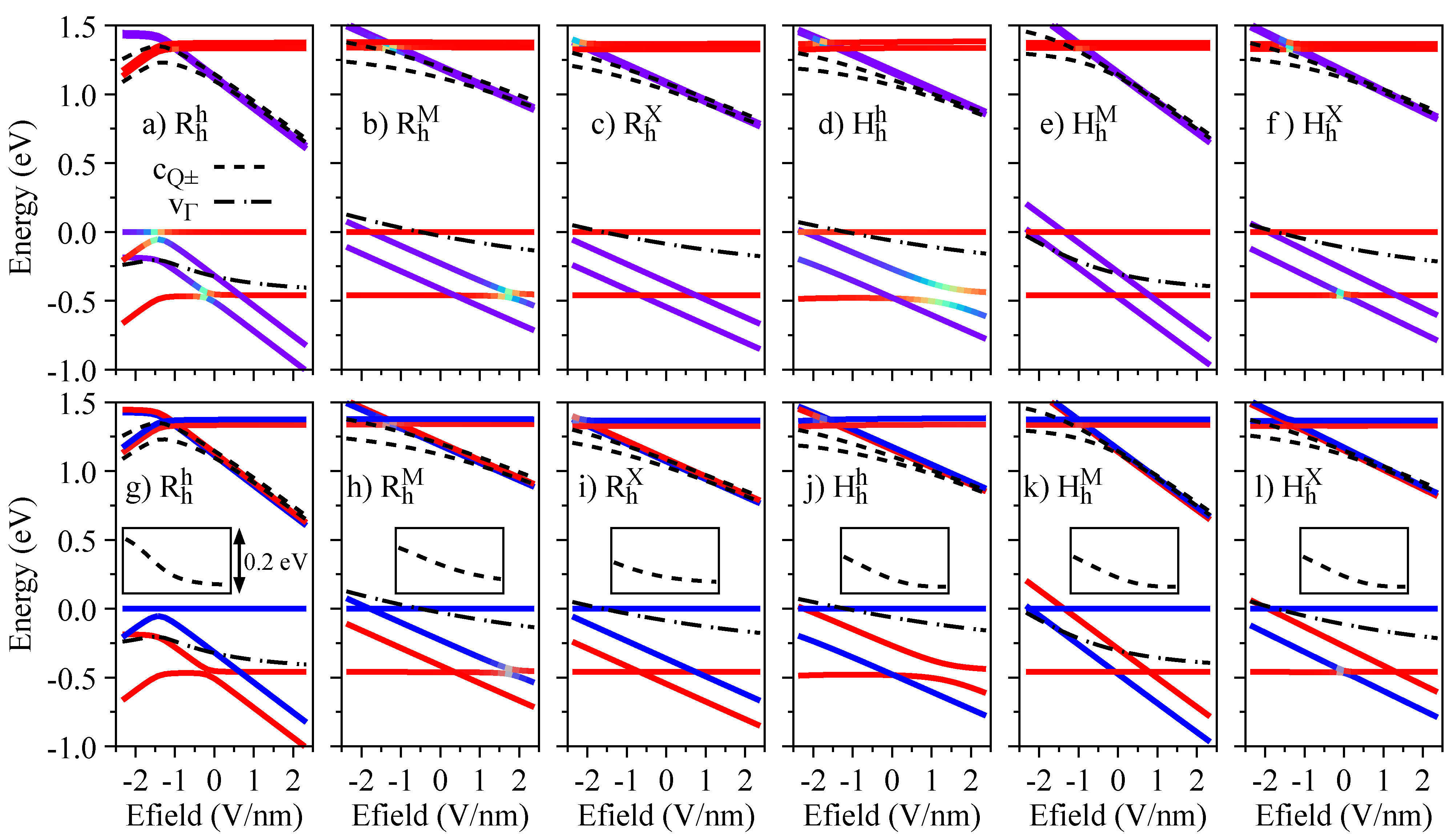
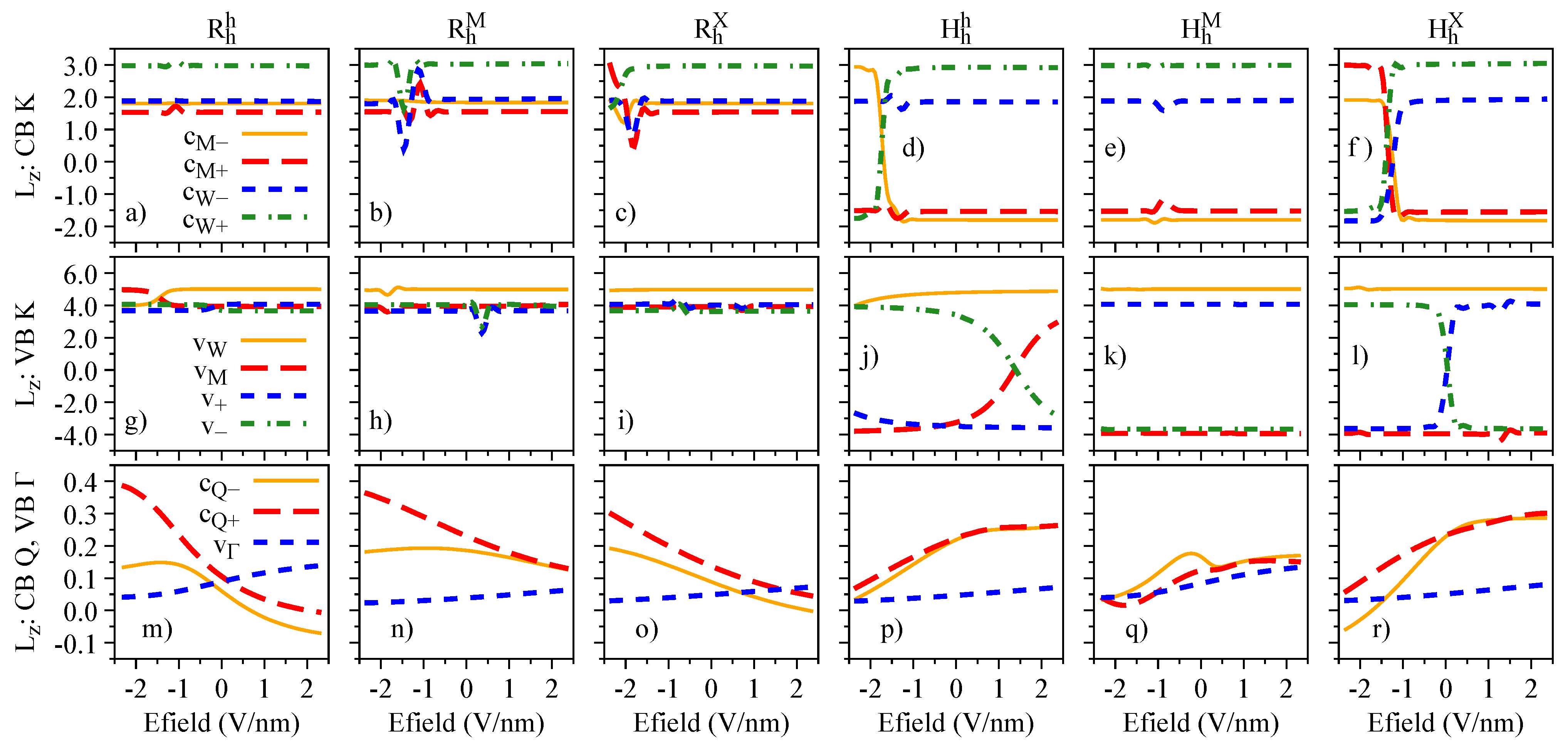
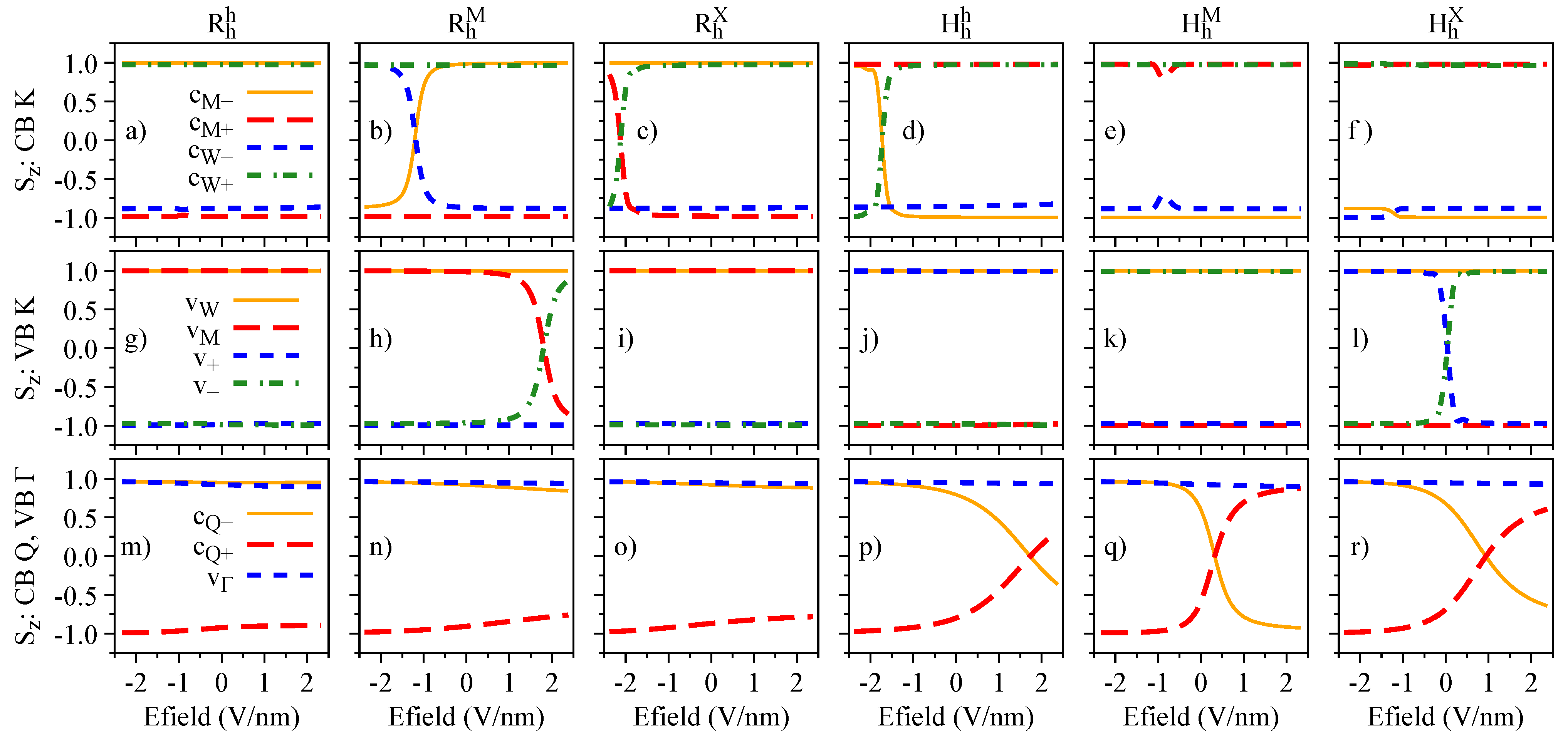
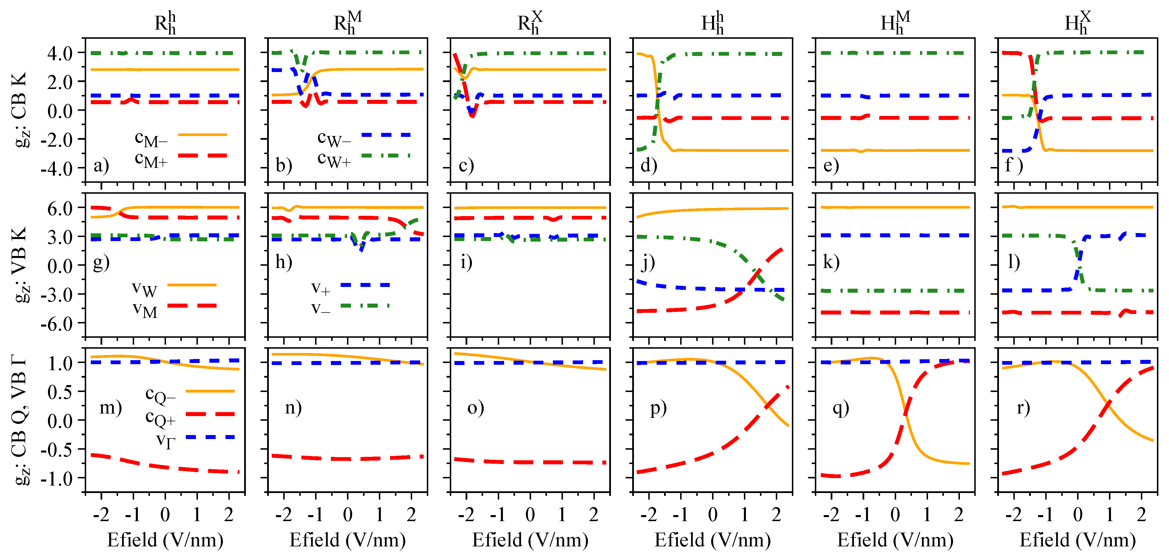
3.2. Electric Field Dependence
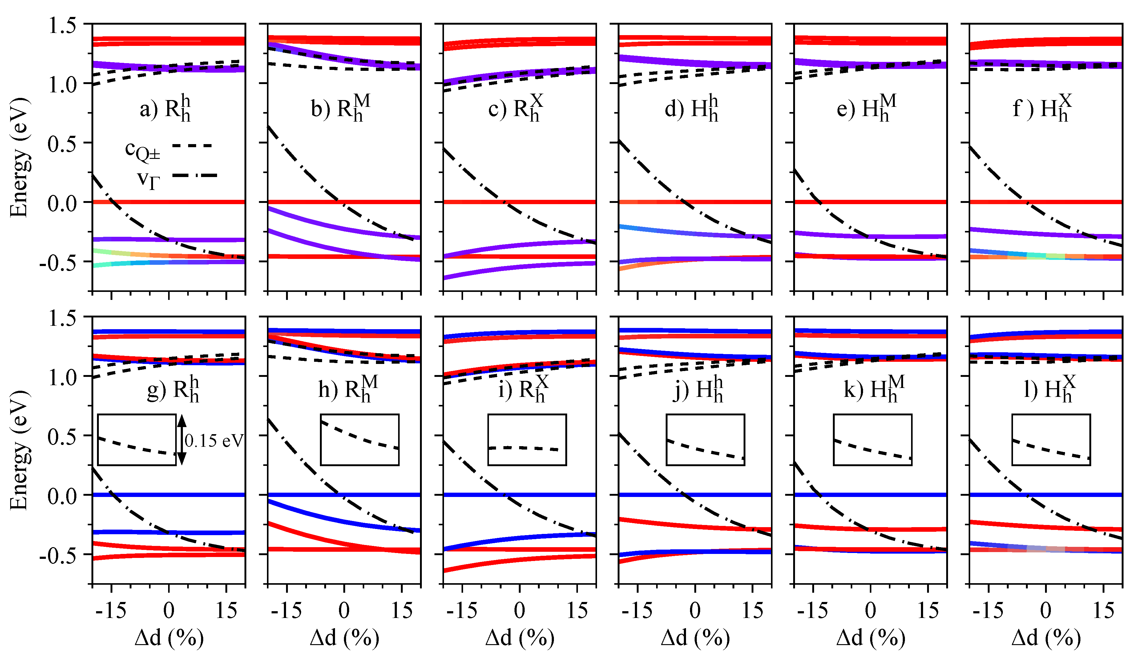
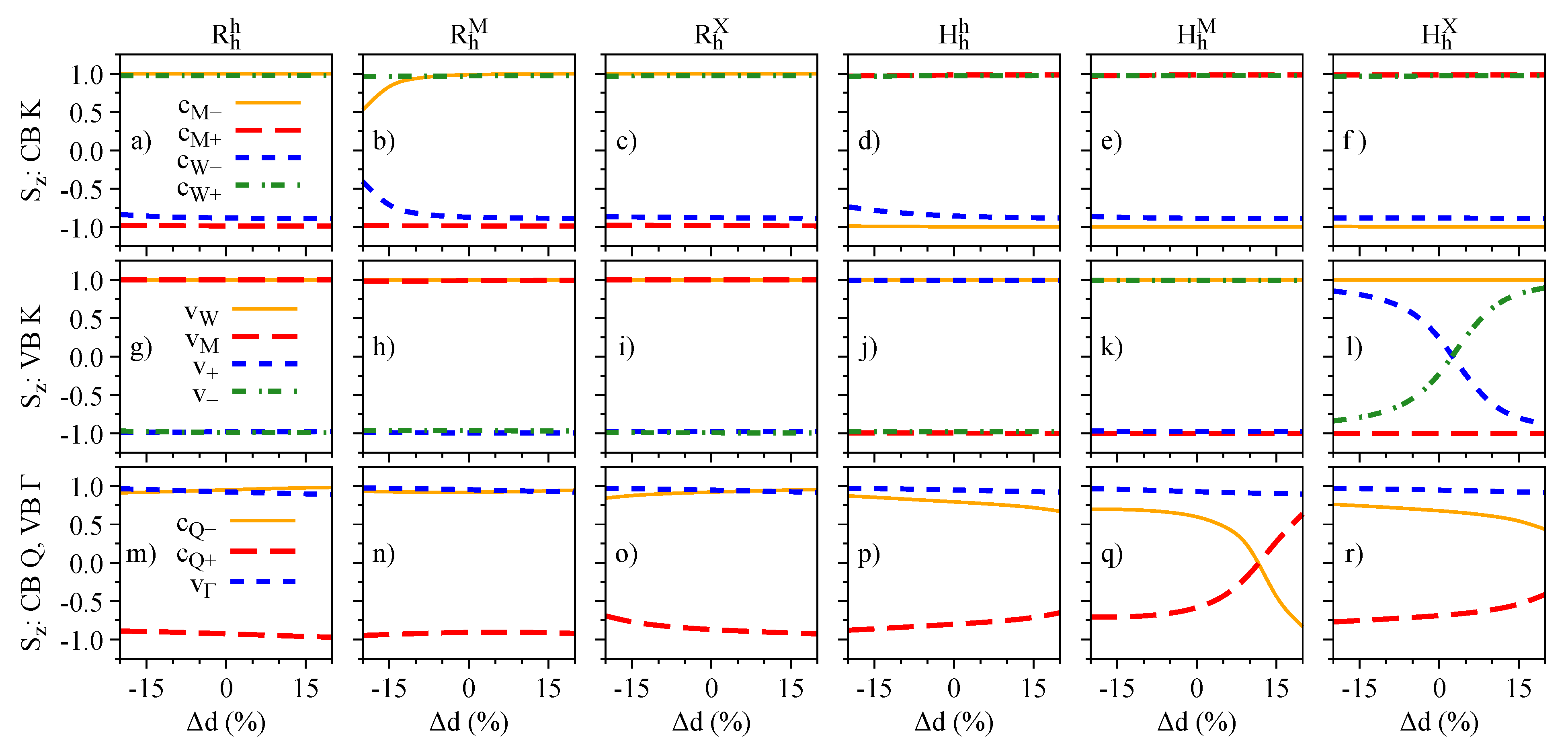
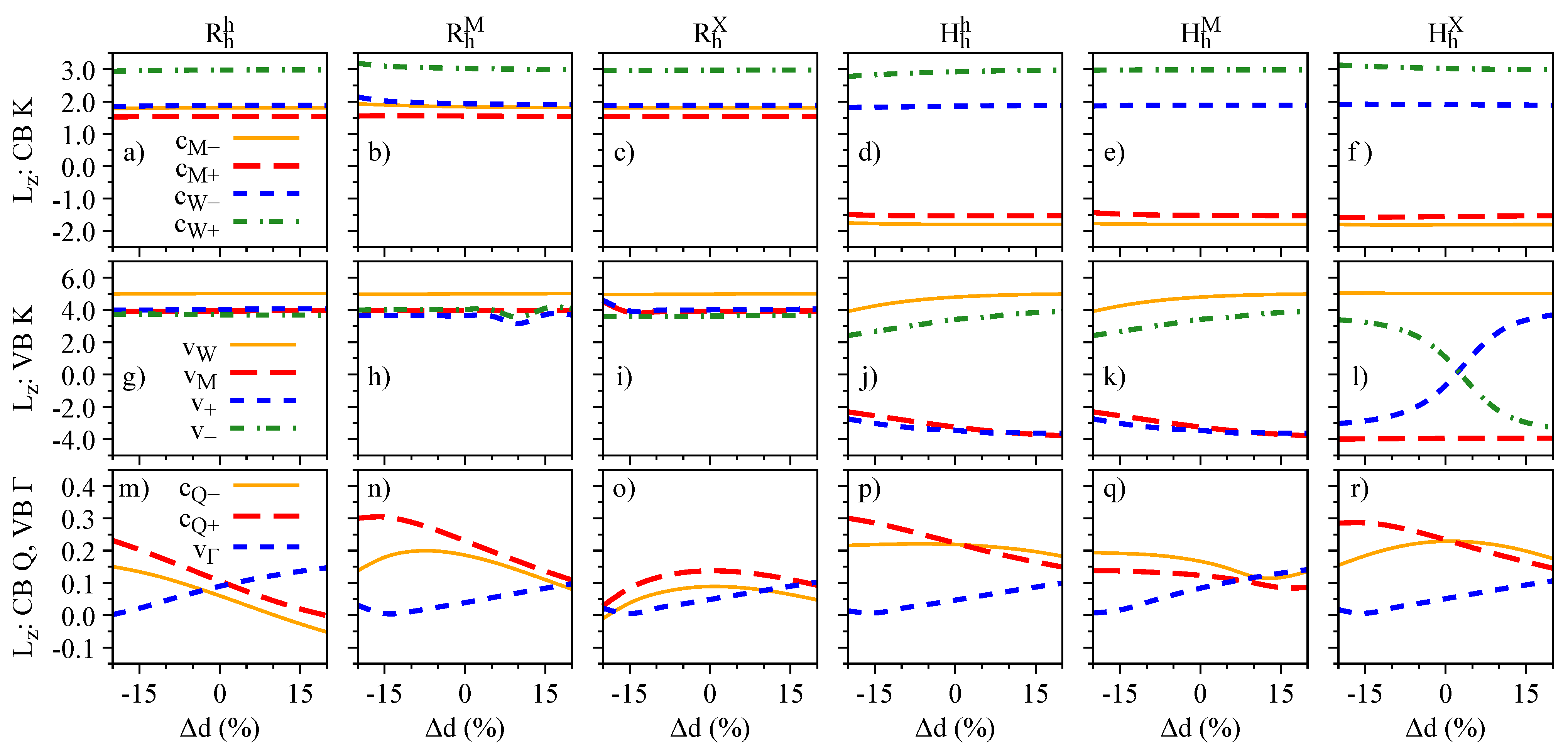
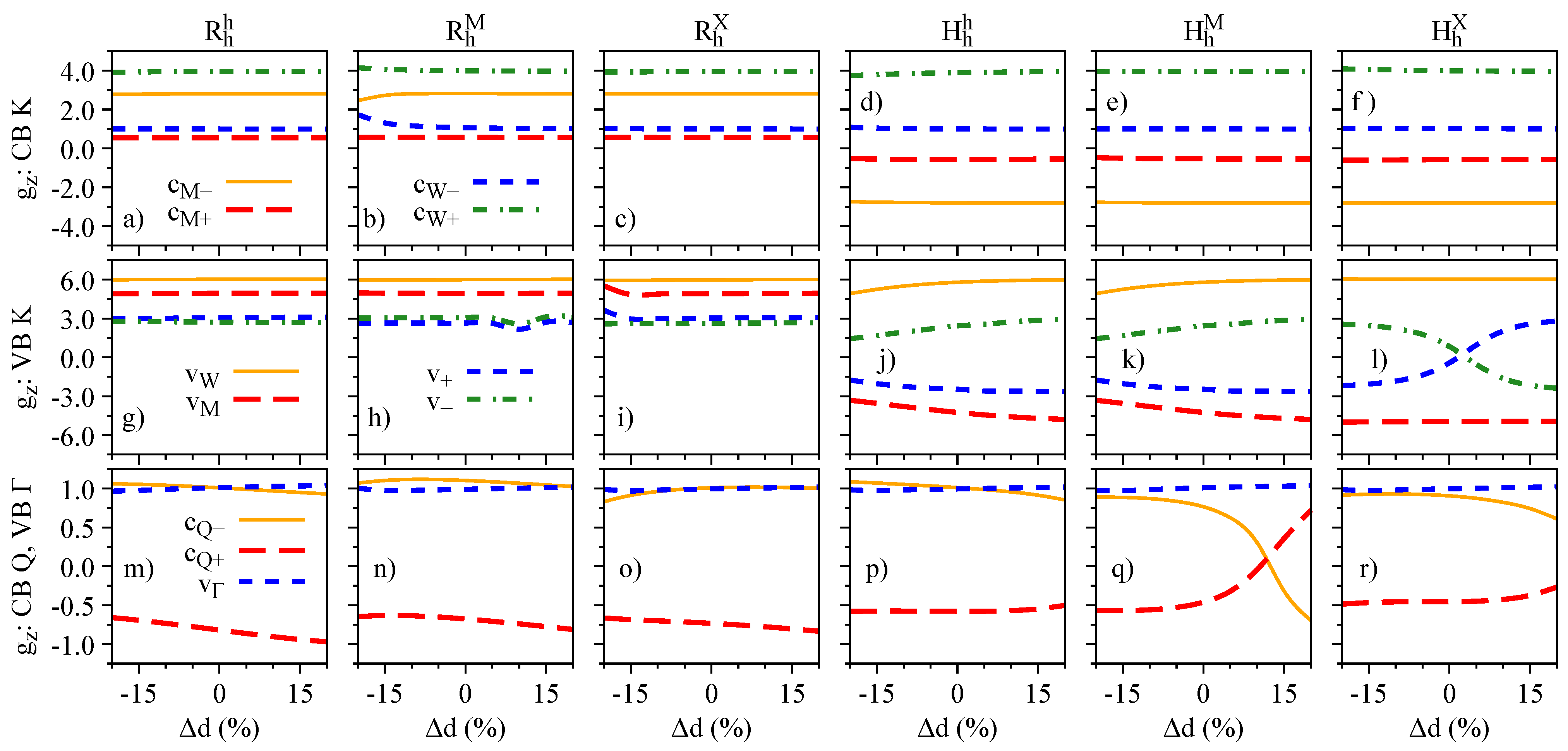
3.3. Interlayer Distance Variation
4. Low-Energy Dipolar Excitons
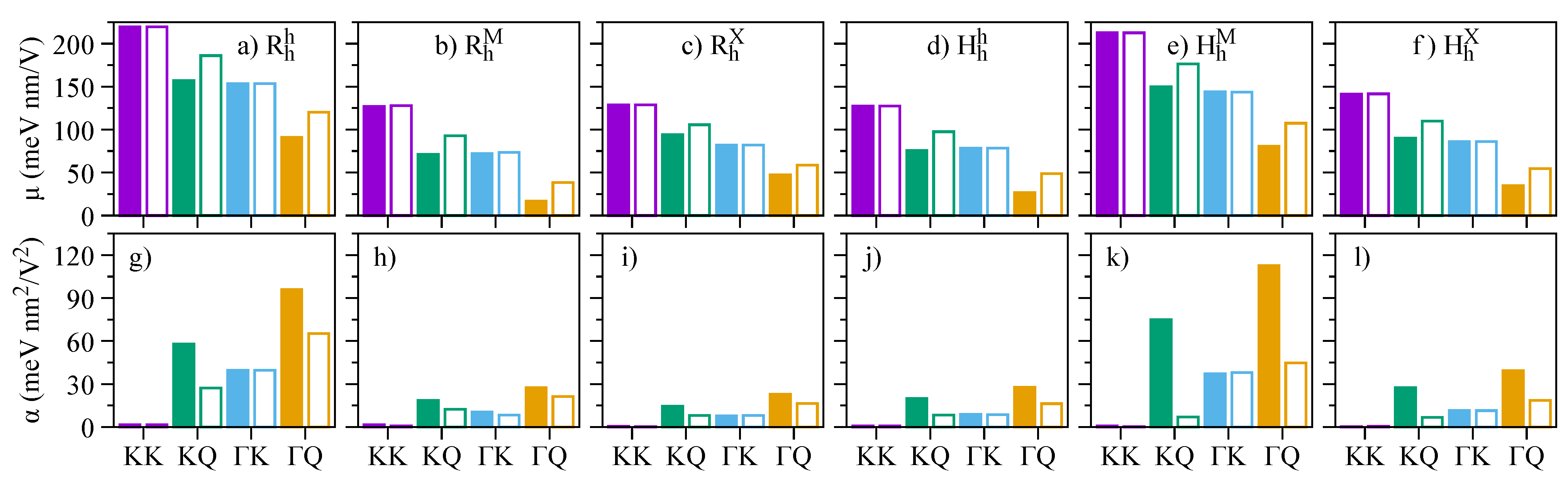
4.1. Symmetry-Based Selection Rules
4.2. Effective g-Factors
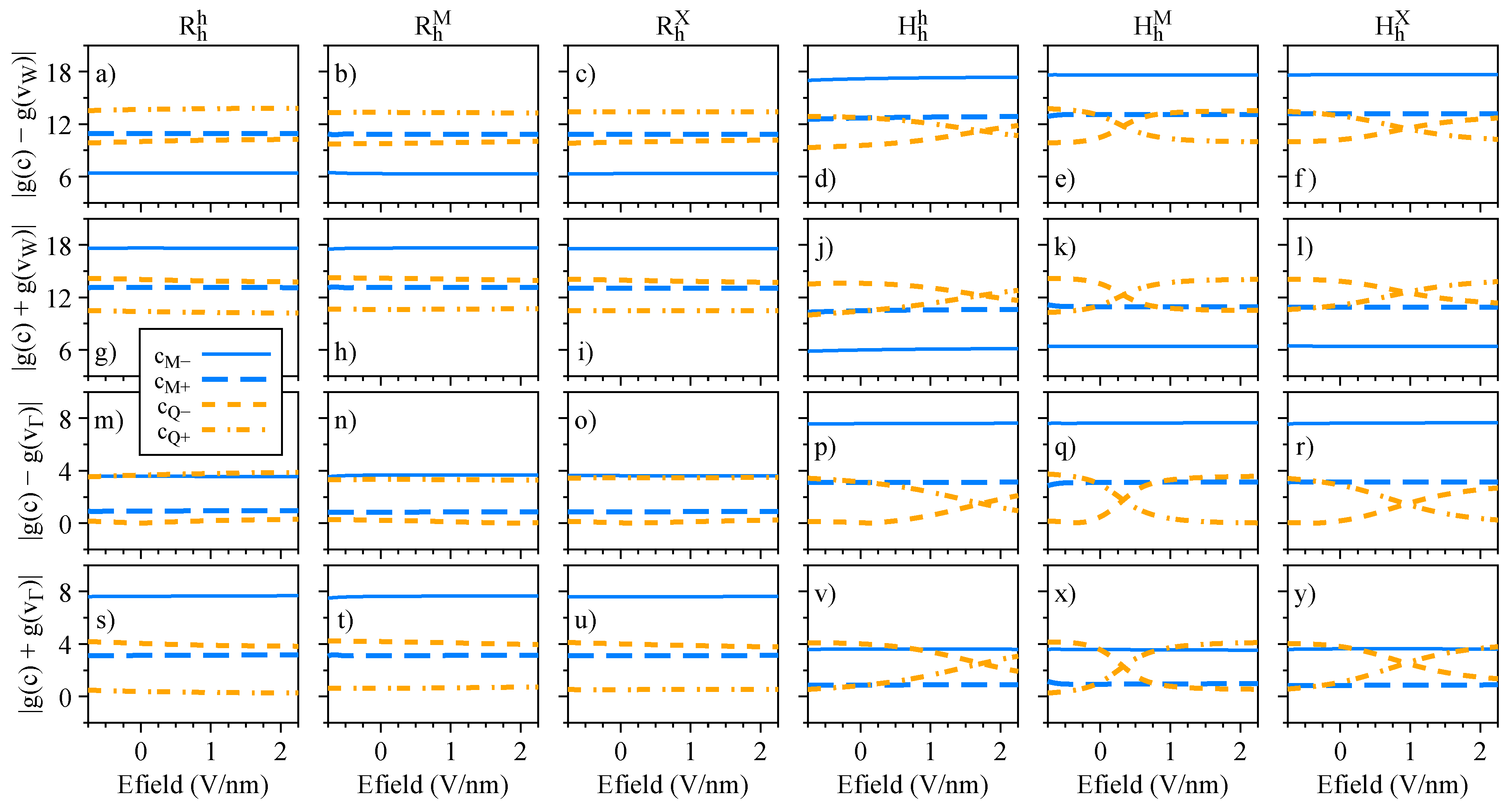
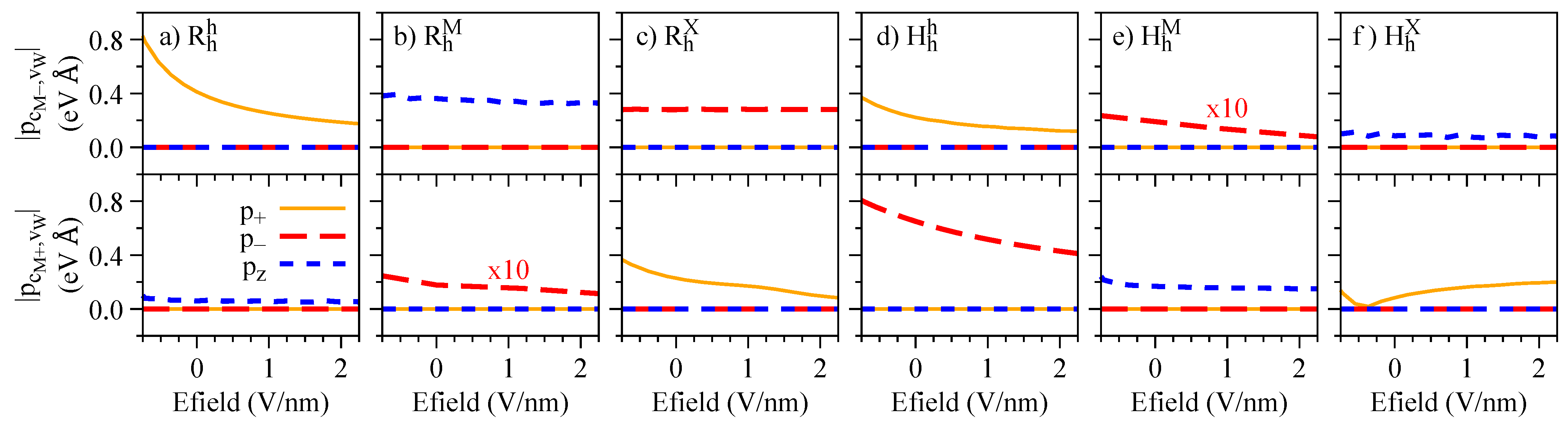
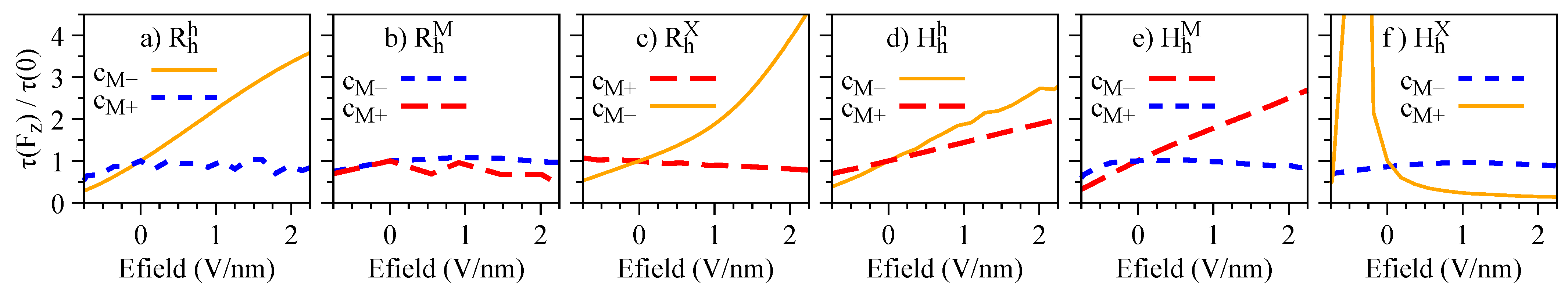
4.3. Electric Field Dependence
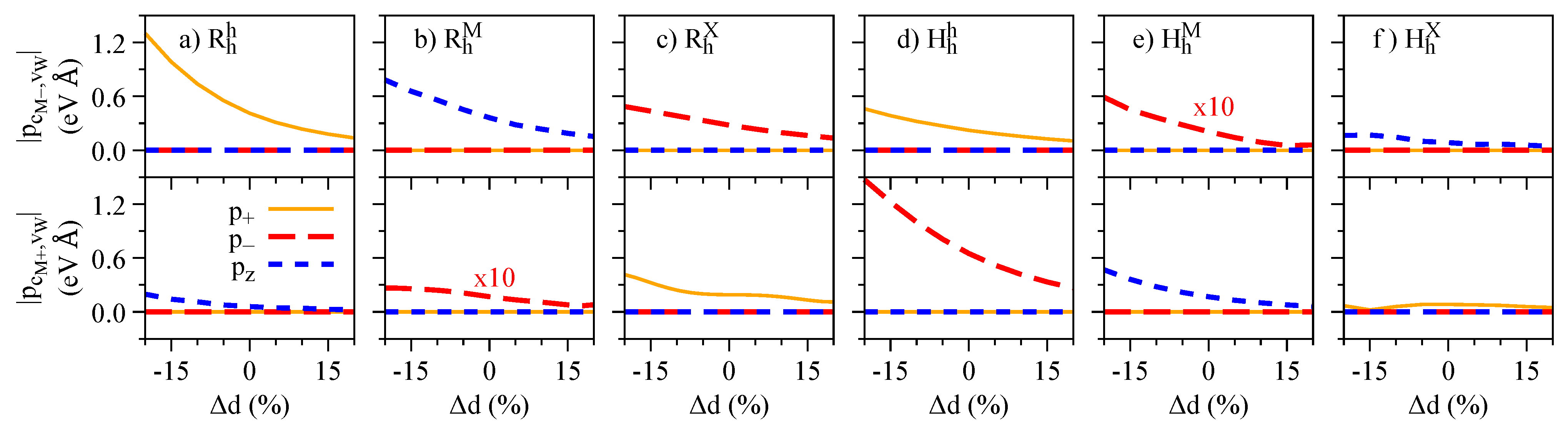
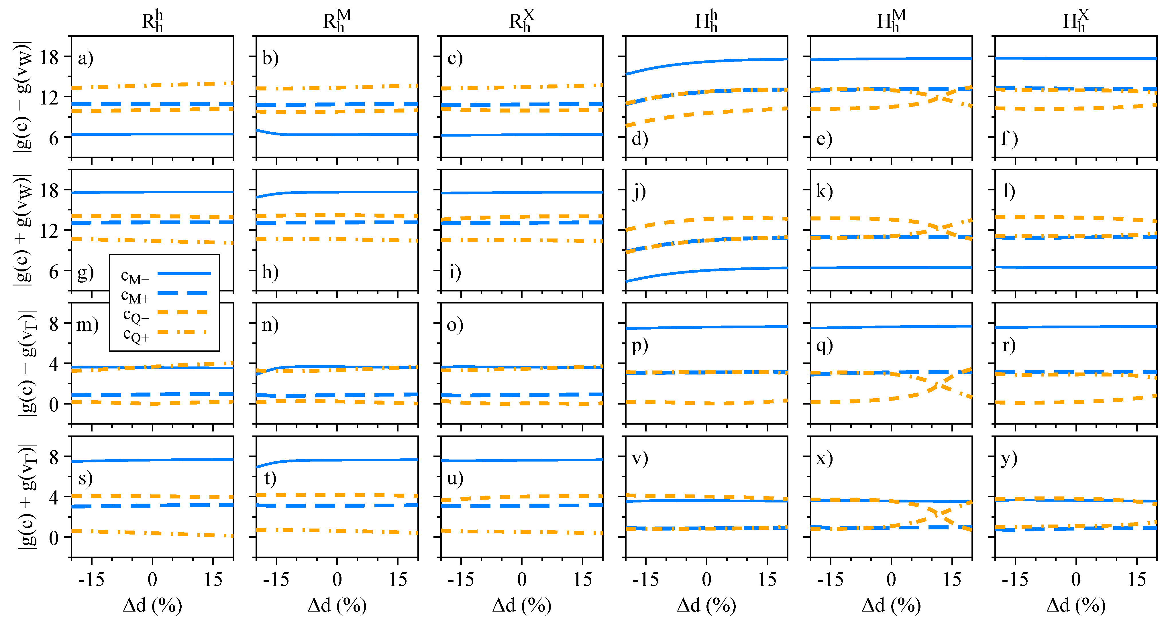
4.4. Interlayer Distance Variation
5. Concluding Remarks
Author Contributions
Funding
Data Availability Statement
Acknowledgments
Conflicts of Interest
Appendix A. Computational Details
References
- Mak, K.F.; Lee, C.; Hone, J.; Shan, J.; Heinz, T.F. Atomically Thin MoS2: A New Direct-Gap Semiconductor. Phys. Rev. Lett. 2010, 105, 136805. [Google Scholar] [CrossRef] [PubMed] [Green Version]
- Splendiani, A.; Sun, L.; Zhang, Y.; Li, T.; Kim, J.; Chim, C.Y.; Galli, G.; Wang, F. Emerging photoluminescence in monolayer MoS2. Nano Lett. 2010, 10, 1271. [Google Scholar] [CrossRef] [PubMed]
- Kuc, A.; Zibouche, N.; Heine, T. Influence of quantum confinement on the electronic structure of the transition metal sulfide TS2. Phys. Rev. B 2011, 83, 245213. [Google Scholar] [CrossRef] [Green Version]
- Kumar, A.; Ahluwalia, P. Electronic structure of transition metal dichalcogenides monolayers 1H-MX2 (M= Mo, W; X= S, Se, Te) from ab-initio theory: New direct band gap semiconductors. Eur. Phys. J. B 2012, 85, 186. [Google Scholar] [CrossRef]
- Xiao, D.; Liu, G.B.; Feng, W.; Xu, X.; Yao, W. Coupled Spin and Valley Physics in Monolayers of MoS2 and Other Group-VI Dichalcogenides. Phys. Rev. Lett. 2012, 108, 196802. [Google Scholar] [CrossRef] [Green Version]
- Mak, K.F.; He, K.; Shan, J.; Heinz, T.F. Control of valley polarization in monolayer MoS2 by optical helicity. Nat. Nanotechnol. 2012, 7, 494. [Google Scholar] [CrossRef]
- Mak, K.F.; McGill, K.L.; Park, J.; McEuen, P.L. The valley Hall effect in MoS2 transistors. Science 2014, 344, 1489. [Google Scholar] [CrossRef] [Green Version]
- Qiu, D.Y.; da Jornada, F.H.; Louie, S.G. Optical Spectrum of MoS2: Many-Body Effects and Diversity of Exciton States. Phys. Rev. Lett. 2013, 111, 216805. [Google Scholar] [CrossRef] [Green Version]
- Xu, X.; Yao, W.; Xiao, D.; Heinz, T.F. Spin and pseudospins in layered transition metal dichalcogenides. Nat. Phys. 2014, 10, 343. [Google Scholar] [CrossRef]
- Chernikov, A.; Berkelbach, T.C.; Hill, H.M.; Rigosi, A.; Li, Y.; Aslan, O.B.; Reichman, D.R.; Hybertsen, M.S.; Heinz, T.F. Exciton Binding Energy and Nonhydrogenic Rydberg Series in Monolayer WS2. Phys. Rev. Lett. 2014, 113, 076802. [Google Scholar] [CrossRef] [Green Version]
- Stier, A.V.; McCreary, K.M.; Jonker, B.T.; Kono, J.; Crooker, S.A. Exciton diamagnetic shifts and valley Zeeman effects in monolayer WS2 and MoS2 to 65 Tesla. Nat. Commun. 2016, 7, 10643. [Google Scholar] [CrossRef] [Green Version]
- Schaibley, J.R.; Yu, H.; Clark, G.; Rivera, P.; Ross, J.S.; Seyler, K.L.; Yao, W.; Xu, X. Valleytronics in 2D materials. Nat. Rev. Mater. 2016, 1, 16055. [Google Scholar] [CrossRef]
- Raja, A.; Chaves, A.; Yu, J.; Arefe, G.; Hill, H.M.; Rigosi, A.F.; Berkelbach, T.C.; Nagler, P.; Schüller, C.; Korn, T.; et al. Coulomb engineering of the bandgap and excitons in two-dimensional materials. Nat. Commun. 2017, 8, 15251. [Google Scholar] [CrossRef] [PubMed] [Green Version]
- Wang, G.; Chernikov, A.; Glazov, M.M.; Heinz, T.F.; Marie, X.; Amand, T.; Urbaszek, B. Colloquium: Excitons in atomically thin transition metal dichalcogenides. Rev. Mod. Phys. 2018, 90, 021001. [Google Scholar] [CrossRef] [Green Version]
- Geim, A.K.; Grigorieva, I.V. Van der Waals heterostructures. Nature 2013, 499, 419. [Google Scholar] [CrossRef] [Green Version]
- Song, J.C.W.; Gabor, N.M. Electron quantum metamaterials in van der Waals heterostructures. Nat. Nanotechnol. 2018, 13, 986. [Google Scholar] [CrossRef] [Green Version]
- Sierra, J.F.; Fabian, J.; Kawakami, R.K.; Roche, S.; Valenzuela, S.O. Van der Waals heterostructures for spintronics and opto-spintronics. Nat. Nanotechnol. 2021, 16, 856. [Google Scholar] [CrossRef]
- Ciarrocchi, A.; Tagarelli, F.; Avsar, A.; Kis, A. Excitonic devices with van der Waals heterostructures: Valleytronics meets twistronics. Nat. Rev. Mater. 2022, 7, 449. [Google Scholar] [CrossRef]
- Tran, K.; Moody, G.; Wu, F.; Lu, X.; Choi, J.; Kim, K.; Rai, A.; Sanchez, D.A.; Quan, J.; Singh, A.; et al. Evidence for moiré excitons in van der Waals heterostructures. Nature 2019, 567, 71. [Google Scholar] [CrossRef] [PubMed] [Green Version]
- Seyler, K.L.; Rivera, P.; Yu, H.; Wilson, N.P.; Ray, E.L.; Mandrus, D.G.; Yan, J.; Yao, W.; Xu, X. Signatures of moiré-trapped valley excitons in MoSe2/WSe2 heterobilayers. Nature 2019, 567, 66. [Google Scholar] [CrossRef] [Green Version]
- Leisgang, N.; Shree, S.; Paradisanos, I.; Sponfeldner, L.; Robert, C.; Lagarde, D.; Balocchi, A.; Watanabe, K.; Taniguchi, T.; Marie, X.; et al. Giant Stark splitting of an exciton in bilayer MoS2. Nat. Nanotechnol. 2020, 15, 901. [Google Scholar] [CrossRef] [PubMed]
- Lin, K.Q.; Faria Junior, P.E.; Bauer, J.M.; Peng, B.; Monserrat, B.; Gmitra, M.; Fabian, J.; Bange, S.; Lupton, J.M. Twist-angle engineering of excitonic quantum interference and optical nonlinearities in stacked 2D semiconductors. Nat. Commun. 2021, 12, 1553. [Google Scholar] [CrossRef]
- Gmitra, M.; Fabian, J. Graphene on transition-metal dichalcogenides: A platform for proximity spin-orbit physics and optospintronics. Phys. Rev. B 2015, 92, 155403. [Google Scholar] [CrossRef] [Green Version]
- Gmitra, M.; Kochan, D.; Högl, P.; Fabian, J. Trivial and inverted Dirac bands and the emergence of quantum spin Hall states in graphene on transition-metal dichalcogenides. Phys. Rev. B 2016, 93, 155104. [Google Scholar] [CrossRef] [Green Version]
- Avsar, A.; Unuchek, D.; Liu, J.; Sanchez, O.L.; Watanabe, K.; Taniguchi, T.; Özyilmaz, B.; Kis, A. Optospintronics in Graphene via Proximity Coupling. ACS Nano 2017, 11, 11678. [Google Scholar] [CrossRef] [PubMed]
- Luo, Y.K.; Xu, J.; Zhu, T.; Wu, G.; McCormick, E.J.; Zhan, W.; Neupane, M.R.; Kawakami, R.K. Opto-Valleytronic Spin Injection in Monolayer MoS2/Few-Layer Graphene Hybrid Spin Valves. Nano Lett. 2017, 17, 3877. [Google Scholar] [CrossRef] [Green Version]
- Faria Junior, P.E.; Naimer, T.; McCreary, K.M.; Jonker, B.T.; Finley, J.J.; Crooker, S.; Fabian, J.; Stier, A.V. Proximity-enhanced valley Zeeman splitting at the WS2/graphene interface. arXiv 2023, arXiv:2301.12234. [Google Scholar]
- Cadiz, F.; Courtade, E.; Robert, C.; Wang, G.; Shen, Y.; Cai, H.; Taniguchi, T.; Watanabe, K.; Carrere, H.; Lagarde, D.; et al. Excitonic Linewidth Approaching the Homogeneous Limit in MoS2-Based van der Waals Heterostructures. Phys. Rev. X 2017, 7, 021026. [Google Scholar] [CrossRef] [Green Version]
- Goryca, M.; Li, J.; Stier, A.V.; Taniguchi, T.; Watanabe, K.; Courtade, E.; Shree, S.; Robert, C.; Urbaszek, B.; Marie, X.; et al. Revealing exciton masses and dielectric properties of monolayer semiconductors with high magnetic fields. Nat. Commun. 2019, 10, 4172. [Google Scholar] [CrossRef] [Green Version]
- Yankowitz, M.; Ma, Q.; Jarillo-Herrero, P.; LeRoy, B.J. van der Waals heterostructures combining graphene and hexagonal boron nitride. Nat. Rev. Phys. 2019, 1, 112. [Google Scholar] [CrossRef]
- Zollner, K.; Faria Junior, P.E.; Fabian, J. Proximity exchange effects in MoSe2 and WSe2 heterostructures with CrI3: Twist angle, layer, and gate dependence. Phys. Rev. B 2019, 100, 085128. [Google Scholar] [CrossRef] [Green Version]
- Zollner, K.; Faria Junior, P.E.; Fabian, J. Strong manipulation of the valley splitting upon twisting and gating in MoSe2/CrI3 and WSe2/CrI3 van der Waals heterostructures. Phys. Rev. B 2023, 107, 035112. [Google Scholar] [CrossRef]
- Zhong, D.; Seyler, K.L.; Linpeng, X.; Cheng, R.; Sivadas, N.; Huang, B.; Schmidgall, E.; Taniguchi, T.; Watanabe, K.; McGuire, M.A.; et al. Van der Waals engineering of ferromagnetic semiconductor heterostructures for spin and valleytronics. Sci. Adv. 2017, 3, e1603113. [Google Scholar] [CrossRef] [PubMed] [Green Version]
- Ciorciaro, L.; Kroner, M.; Watanabe, K.; Taniguchi, T.; Imamoglu, A. Observation of magnetic proximity effect using resonant optical spectroscopy of an electrically tunable MoSe2/CrBr3 heterostructure. Phys. Rev. Lett. 2020, 124, 197401. [Google Scholar] [CrossRef] [PubMed]
- Choi, J.; Lane, C.; Zhu, J.X.; Crooker, S.A. Asymmetrict magnetic proximity interactions in MoSe2/CrBr3 van der Waals heterostructures. Nat. Mater. 2022, 22, 305–310. [Google Scholar] [CrossRef] [PubMed]
- Chaves, A.; Azadani, J.G.; Özçelik, V.O.; Grassi, R.; Low, T. Electrical control of excitons in van der Waals heterostructures with type-II band alignment. Phys. Rev. B 2018, 98, 121302. [Google Scholar] [CrossRef] [Green Version]
- Gillen, R.; Maultzsch, J. Interlayer excitons in MoSe2/WSe2 heterostructures from first principles. Phys. Rev. B 2018, 97, 165306. [Google Scholar] [CrossRef] [Green Version]
- Torun, E.; Miranda, H.P.C.; Molina-Sánchez, A.; Wirtz, L. Interlayer and intralayer excitons in MoS2/WS2 and MoSe2/WSe2 heterobilayers. Phys. Rev. B 2018, 97, 245427. [Google Scholar] [CrossRef] [Green Version]
- Rivera, P.; Schaibley, J.R.; Jones, A.M.; Ross, J.S.; Wu, S.; Aivazian, G.; Klement, P.; Seyler, K.; Clark, G.; Ghimire, N.J.; et al. Observation of long-lived interlayer excitons in monolayer MoSe2–WSe2 heterostructures. Nat. Commun. 2015, 6, 6242. [Google Scholar] [CrossRef] [Green Version]
- Miller, B.; Steinhoff, A.; Pano, B.; Klein, J.; Jahnke, F.; Holleitner, A.; Wurstbauer, U. Long-Lived Direct and Indirect Interlayer Excitons in van der Waals Heterostructures. Nano Lett. 2017, 17, 5229. [Google Scholar] [CrossRef] [Green Version]
- Nagler, P.; Plechinger, G.; Ballottin, M.V.; Mitioglu, A.; Meier, S.; Paradiso, N.; Strunk, C.; Chernikov, A.; Christianen, P.C.M.; Schüller, C.; et al. Interlayer exciton dynamics in a dichalcogenide monolayer heterostructure. 2D Mater. 2017, 4, 025112. [Google Scholar] [CrossRef] [Green Version]
- Ciarrocchi, A.; Unuchek, D.; Avsar, A.; Watanabe, K.; Taniguchi, T.; Kis, A. Polarization switching and electrical control of interlayer excitons in two-dimensional van der Waals heterostructures. Nat. Photonics 2019, 13, 131. [Google Scholar] [CrossRef]
- Baek, H.; Brotons-Gisbert, M.; Koong, Z.X.; Campbell, A.; Rambach, M.; Watanabe, K.; Taniguchi, T.; Gerardot, B.D. Highly energy-tunable quantum light from moiré-trapped excitons. Sci. Adv. 2020, 6, eaba8526. [Google Scholar] [CrossRef] [PubMed]
- Shanks, D.N.; Mahdikhanysarvejahany, F.; Muccianti, C.; Alfrey, A.; Koehler, M.R.; Mandrus, D.G.; Taniguchi, T.; Watanabe, K.; Yu, H.; LeRoy, B.J.; et al. Nanoscale Trapping of Interlayer Excitons in a 2D Semiconductor Heterostructure. Nano Lett. 2021, 21, 5641. [Google Scholar] [CrossRef] [PubMed]
- Barré, E.; Karni, O.; Liu, E.; O’Beirne, A.L.; Chen, X.; Ribeiro, H.B.; Yu, L.; Kim, B.; Watanabe, K.; Taniguchi, T.; et al. Optical absorption of interlayer excitons in transition-metal dichalcogenide heterostructures. Science 2022, 376, 406. [Google Scholar] [CrossRef]
- Shanks, D.N.; Mahdikhanysarvejahany, F.; Stanfill, T.G.; Koehler, M.R.; Mandrus, D.G.; Taniguchi, T.; Watanabe, K.; LeRoy, B.J.; Schaibley, J.R. Interlayer Exciton Diode and Transistor. Nano Lett. 2022, 22, 6599. [Google Scholar] [CrossRef] [PubMed]
- Nagler, P.; Ballottin, M.V.; Mitioglu, A.A.; Mooshammer, F.; Paradiso, N.; Strunk, C.; Huber, R.; Chernikov, A.; Christianen, P.C.M.; Schüller, C.; et al. Giant magnetic splitting inducing near-unity valley polarization in van der Waals heterostructures. Nat. Commun. 2017, 8, 1551. [Google Scholar] [CrossRef] [Green Version]
- Mahdikhanysarvejahany, F.; Shanks, D.N.; Muccianti, C.; Badada, B.H.; Idi, I.; Alfrey, A.; Raglow, S.; Koehler, M.R.; Mandrus, D.G.; Taniguchi, T.; et al. Temperature dependent moiré trapping of interlayer excitons in MoSe2-WSe2 heterostructures. Npj 2D Mater. Appl. 2021, 5, 67. [Google Scholar] [CrossRef]
- Holler, J.; Selig, M.; Kempf, M.; Zipfel, J.; Nagler, P.; Katzer, M.; Katsch, F.; Ballottin, M.V.; Mitioglu, A.A.; Chernikov, A.; et al. Interlayer exciton valley polarization dynamics in large magnetic fields. Phys. Rev. B 2022, 105, 085303. [Google Scholar] [CrossRef]
- Smirnov, D.S.; Holler, J.; Kempf, M.; Zipfel, J.; Nagler, P.; Ballottin, M.V.; Mitioglu, A.A.; Chernikov, A.; Christianen, P.C.M.; Schüller, C.; et al. Valley-magnetophonon resonance for interlayer excitons. 2D Mater. 2022, 9, 045016. [Google Scholar] [CrossRef]
- Li, Z.; Tabataba-Vakili, F.; Zhao, S.; Rupp, A.; Bilgin, I.; Herdegen, Z.; März, B.; Watanabe, K.; Taniguchi, T.; Schleder, G.R.; et al. Lattice reconstruction in MoSe2-WSe2 heterobilayers synthesized by chemical vapor deposition. arXiv 2022, arXiv:2212.07686. [Google Scholar]
- Choi, J.; Florian, M.; Steinhoff, A.; Erben, D.; Tran, K.; Kim, D.S.; Sun, L.; Quan, J.; Claassen, R.; Majumder, S.; et al. Twist Angle-Dependent Interlayer Exciton Lifetimes in van der Waals Heterostructures. Phys. Rev. Lett. 2021, 126, 047401. [Google Scholar] [CrossRef]
- Förg, M.; Baimuratov, A.S.; Kruchinin, S.Y.; Vovk, I.A.; Scherzer, J.; Förste, J.; Funk, V.; Watanabe, K.; Taniguchi, T.; Högele, A. Moiré excitons in MoSe2-WSe2 heterobilayers and heterotrilayers. Nat. Commun. 2021, 12, 1656. [Google Scholar] [CrossRef] [PubMed]
- Enaldiev, V.V.; Zólyomi, V.; Yelgel, C.; Magorrian, S.J.; Fal’ko, V.I. Stacking Domains and Dislocation Networks in Marginally Twisted Bilayers of Transition Metal Dichalcogenides. Phys. Rev. Lett. 2020, 124, 206101. [Google Scholar] [CrossRef]
- Holler, J.; Meier, S.; Kempf, M.; Nagler, P.; Watanabe, K.; Taniguchi, T.; Korn, T.; Schüller, C. Low-frequency Raman scattering in WSe2-MoSe2 heterobilayers: Evidence for atomic reconstruction. Appl. Phys. Lett. 2020, 117, 013104. [Google Scholar] [CrossRef]
- Parzefall, P.; Holler, J.; Scheuck, M.; Beer, A.; Lin, K.Q.; Peng, B.; Monserrat, B.; Nagler, P.; Kempf, M.; Korn, T.; et al. Moiré phonons in twisted MoSe2–WSe2 heterobilayers and their correlation with interlayer excitons. 2D Mater. 2021, 8, 035030. [Google Scholar] [CrossRef]
- Zhao, S.; Huang, X.; Li, Z.; Rupp, A.; Göser, J.; Vovk, I.A.; Kruchinin, S.Y.; Watanabe, K.; Taniguchi, T.; Bilgin, I.; et al. Excitons in mesoscopically reconstructed moiré hetersotructures. arXiv 2022, arXiv:2202.11139. [Google Scholar]
- Hanbicki, A.T.; Chuang, H.J.; Rosenberger, M.R.; Hellberg, C.S.; Sivaram, S.V.; McCreary, K.M.; Mazin, I.I.; Jonker, B.T. Double Indirect Interlayer Exciton in a MoSe2/WSe2 van der Waals Heterostructure. ACS Nano 2018, 12, 4719. [Google Scholar] [CrossRef] [Green Version]
- Sigl, L.; Sigger, F.; Kronowetter, F.; Kiemle, J.; Klein, J.; Watanabe, K.; Taniguchi, T.; Finley, J.J.; Wurstbauer, U.; Holleitner, A.W. Signatures of a degenerate many-body state of interlayer excitons in a van der Waals heterostack. Phys. Rev. Res. 2020, 2, 042044. [Google Scholar] [CrossRef]
- Wang, T.; Miao, S.; Li, Z.; Meng, Y.; Lu, Z.; Lian, Z.; Blei, M.; Taniguchi, T.; Watanabe, K.; Tongay, S.; et al. Giant Valley-Zeeman Splitting from Spin-Singlet and Spin-Triplet Interlayer Excitons in WSe2/MoSe2 Heterostructure. Nano Lett. 2020, 20, 694. [Google Scholar] [CrossRef] [Green Version]
- Delhomme, A.; Vaclavkova, D.; Slobodeniuk, A.; Orlita, M.; Potemski, M.; Basko, D.M.; Watanabe, K.; Taniguchi, T.; Mauro, D.; Barreteau, C.; et al. Flipping exciton angular momentum with chiral phonons in MoSe2/WSe2 heterobilayers. 2D Mater. 2020, 7, 041002. [Google Scholar] [CrossRef]
- Ramasubramaniam, A.; Naveh, D.; Towe, E. Tunable band gaps in bilayer transition-metal dichalcogenides. Phys. Rev. B 2011, 84, 205325. [Google Scholar] [CrossRef]
- Plankl, M.; Faria Junior, P.E.; Mooshammer, F.; Siday, T.; Zizlsperger, M.; Sandner, F.; Schiegl, F.; Maier, S.; Huber, M.A.; Gmitra, M.; et al. Subcycle contact-free nanoscopy of ultrafast interlayer transport in atomically thin heterostructures. Nat. Photonics 2021, 15, 594. [Google Scholar] [CrossRef]
- Woźniak, T.; Faria Junior, P.E.; Seifert, G.; Chaves, A.; Kunstmann, J. Exciton g factors of van der Waals heterostructures from first-principles calculations. Phys. Rev. B 2020, 101, 235408. [Google Scholar] [CrossRef]
- Deilmann, T.; Krüger, P.; Rohlfing, M. Ab Initio Studies of Exciton g Factors: Monolayer Transition Metal Dichalcogenides in Magnetic Fields. Phys. Rev. Lett. 2020, 124, 226402. [Google Scholar] [CrossRef]
- Förste, J.; Tepliakov, N.V.; Kruchinin, S.Y.; Lindlau, J.; Funk, V.; Förg, M.; Watanabe, K.; Taniguchi, T.; Baimuratov, A.S.; Högele, A. Exciton g-factors in monolayer and bilayer WSe2 from experiment and theory. Nat. Commun. 2020, 11, 4539. [Google Scholar] [CrossRef]
- Xuan, F.; Quek, S.Y. Valley Zeeman effect and Landau levels in two-dimensional transition metal dichalcogenides. Phys. Rev. Res. 2020, 2, 033256. [Google Scholar] [CrossRef]
- Yu, H.; Wang, Y.; Tong, Q.; Xu, X.; Yao, W. Anomalous Light Cones and Valley Optical Selection Rules of Interlayer Excitons in Twisted Heterobilayers. Phys. Rev. Lett. 2015, 115, 187002. [Google Scholar] [CrossRef] [Green Version]
- Yu, H.; Liu, G.B.; Tang, J.; Xu, X.; Yao, W. Moiré excitons: From programmable quantum emitter arrays to spin-orbit–coupled artificial lattices. Sci. Adv. 2017, 3, e1701696. [Google Scholar] [CrossRef] [Green Version]
- Nieken, R.; Roche, A.; Mahdikhanysarvejahany, F.; Taniguchi, T.; Watanabe, K.; Koehler, M.R.; Mandrus, D.G.; Schaibley, J.; LeRoy, B.J. Direct STM measurements of R-type and H-type twisted MoSe2/WSe2. APL Mater. 2022, 10, 031107. [Google Scholar] [CrossRef]
- Wu, F.; Lovorn, T.; MacDonald, A.H. Topological Exciton Bands in Moiré Heterojunctions. Phys. Rev. Lett. 2017, 118, 147401. [Google Scholar] [CrossRef] [PubMed] [Green Version]
- Yu, H.; Liu, G.B.; Yao, W. Brightened spin-triplet interlayer excitons and optical selection rules in van der Waals heterobilayers. 2D Mater. 2018, 5, 035021. [Google Scholar] [CrossRef] [Green Version]
- Wu, F.; Lovorn, T.; MacDonald, A.H. Theory of optical absorption by interlayer excitons in transition metal dichalcogenide heterobilayers. Phys. Rev. B 2018, 97, 035306. [Google Scholar] [CrossRef] [Green Version]
- Ruiz-Tijerina, D.A.; Soltero, I.; Mireles, F. Theory of moiré localized excitons in transition metal dichalcogenide heterobilayers. Phys. Rev. B 2020, 102, 195403. [Google Scholar] [CrossRef]
- Erkensten, D.; Brem, S.; Malic, E. Exciton-exciton interaction in transition metal dichalcogenide monolayers and van der Waals heterostructures. Phys. Rev. B 2021, 103, 045426. [Google Scholar] [CrossRef]
- Kormányos, A.; Burkard, G.; Gmitra, M.; Fabian, J.; Zólyomi, V.; Drummond, N.D.; Fal’ko, V. k· p theory for two-dimensional transition metal dichalcogenide semiconductors. 2D Mater. 2015, 2, 022001. [Google Scholar] [CrossRef]
- Zollner, K.; Faria Junior, P.E.; Fabian, J. Strain-tunable orbital, spin-orbit, and optical properties of monolayer transition-metal dichalcogenides. Phys. Rev. B 2019, 100, 195126. [Google Scholar] [CrossRef] [Green Version]
- Nayak, P.K.; Horbatenko, Y.; Ahn, S.; Kim, G.; Lee, J.U.; Ma, K.Y.; Jang, A.R.; Lim, H.; Kim, D.; Ryu, S.; et al. Probing evolution of twist-angle-dependent interlayer excitons in MoSe2/WSe2 van der Waals heterostructures. ACS Nano 2017, 11, 4041. [Google Scholar] [CrossRef]
- Xu, K.; Xu, Y.; Zhang, H.; Peng, B.; Shao, H.; Ni, G.; Li, J.; Yao, M.; Lu, H.; Zhu, H.; et al. The role of Anderson’s rule in determining electronic, optical and transport properties of transition metal dichalcogenide heterostructures. Phys. Chem. Chem. Phys. 2018, 20, 30351. [Google Scholar] [CrossRef] [Green Version]
- Gillen, R. Interlayer Excitonic Spectra of Vertically Stacked MoSe2/WSe2 Heterobilayers. Phys. Status Solidi (b) 2021, 258, 2000614. [Google Scholar] [CrossRef]
- Blaha, P.; Schwarz, K.; Tran, F.; Laskowski, R.; Madsen, G.K.; Marks, L.D. WIEN2k: An APW+lo program for calculating the properties of solids. J. Chem. Phys. 2020, 152, 074101. [Google Scholar] [CrossRef] [Green Version]
- Song, Y.; Dery, H. Transport Theory of Monolayer Transition-Metal Dichalcogenides through Symmetry. Phys. Rev. Lett. 2013, 111, 026601. [Google Scholar] [CrossRef] [Green Version]
- Dery, H.; Song, Y. Polarization analysis of excitons in monolayer and bilayer transition-metal dichalcogenides. Phys. Rev. B 2015, 92, 125431. [Google Scholar] [CrossRef] [Green Version]
- Gilardoni, C.M.; Hendriks, F.; van der Wal, C.H.; Guimarães, M.H.D. Symmetry and control of spin-scattering processes in two-dimensional transition metal dichalcogenides. Phys. Rev. B 2021, 103, 115410. [Google Scholar] [CrossRef]
- Blundo, E.; Faria Junior, P.E.; Surrente, A.; Pettinari, G.; Prosnikov, M.A.; Olkowska-Pucko, K.; Zollner, K.; Woźniak, T.; Chaves, A.; Kazimierczuk, T.; et al. Strain-Induced Exciton Hybridization in WS2 Monolayers Unveiled by Zeeman-Splitting Measurements. Phys. Rev. Lett. 2022, 129, 067402. [Google Scholar] [CrossRef]
- Dresselhaus, G. Spin-Orbit Coupling Effects in Zinc Blende Structures. Phys. Rev. 1955, 100, 580. [Google Scholar] [CrossRef]
- Kane, E.O. Physics of III-V Compounds; Semiconductors and Semimetals; Academic Press: New York, NY, USA, 1966; Volume 1. [Google Scholar] [CrossRef]
- Kane, E.O. Band structure of indium antimonide. J. Phys. Chem. Solids 1957, 1, 249. [Google Scholar] [CrossRef]
- Dresselhaus, M.S.; Dresselhaus, G.; Jorio, A. Group Theory: Application to the Physics of Condensed Matter; Springer Science & Business Media: Berlin/Heidelberg, Germany, 2007. [Google Scholar]
- Lew Yan Voon, L.C.; Willatzen, M. The k.p Method: Electronic Properties of Semiconductors; Springer: Berlin, Germany, 2009. [Google Scholar]
- Koster, G.F.; Dimmock, J.O.; Wheeler, R.G.; Statz, H. Properties of the Thirty-Two Point Groups; MIT Press: Cambridge, MA, USA, 1963; Volume 24. [Google Scholar]
- Xuan, F.; Quek, S.Y. Valley-filling instability and critical magnetic field for interaction-enhanced Zeeman response in doped WSe2 monolayers. Npj Comput. Mater. 2021, 7, 198. [Google Scholar] [CrossRef]
- Heißenbüttel, M.C.; Deilmann, T.; Krüger, P.; Rohlfing, M. Valley-Dependent Interlayer Excitons in Magnetic WSe2/CrI3. Nano Lett. 2021, 21, 5173–5178. [Google Scholar] [CrossRef]
- Covre, F.S.; Faria Junior, P.E.; Gordo, V.O.; de Brito, C.S.; Zhumagulov, Y.V.; Teodoro, M.D.; Couto, O.D.D.; Misoguti, L.; Pratavieira, S.; Andrade, M.B.; et al. Revealing the impact of strain in the optical properties of bubbles in monolayer MoSe2. Nanoscale 2022, 14, 5758. [Google Scholar] [CrossRef] [PubMed]
- Faria Junior, P.E.; Zollner, K.; Woźniak, T.; Kurpas, M.; Gmitra, M.; Fabian, J. First-principles insights into the spin-valley physics of strained transition metal dichalcogenides monolayers. New J. Phys. 2022, 24, 083004. [Google Scholar] [CrossRef]
- Raiber, S.; Faria Junior, P.E.; Falter, D.; Feldl, S.; Marzena, P.; Watanabe, K.; Taniguchi, T.; Fabian, J.; Schüller, C. Ultrafast pseudospin quantum beats in multilayer WSe2 and MoSe2. Nat. Commun. 2022, 13, 4997. [Google Scholar] [CrossRef] [PubMed]
- Amit, T.; Hernangómez-Pérez, D.; Cohen, G.; Qiu, D.Y.; Refaely-Abramson, S. Tunable magneto-optical properties in MoS2 via defect-induced exciton transitions. Phys. Rev. B 2022, 106, L161407. [Google Scholar] [CrossRef]
- Hötger, A.; Amit, T.; Klein, J.; Barthelmi, K.; Pelini, T.; Delhomme, A.; Rey, S.; Potemski, M.; Faugeras, C.; Cohen, G.; et al. Spin-defect characteristics of single sulfur vacancies in monolayer MoS2. arXiv 2022, arXiv:2205.10286. [Google Scholar]
- Gobato, Y.G.; de Brito, C.S.; Chaves, A.; Prosnikov, M.A.; Woźniak, T.; Guo, S.; Barcelos, I.D.; Milošević, M.V.; Withers, F.; Christianen, P.C.M. Distinctive g-Factor of Moiré-Confined Excitons in van der Waals Heterostructures. Nano Lett. 2022, 22, 8641. [Google Scholar] [CrossRef]
- Lejaeghere, K.; Bihlmayer, G.; Björkman, T.; Blaha, P.; Blügel, S.; Blum, V.; Caliste, D.; Castelli, I.E.; Clark, S.J.; Corso, A.D.; et al. Reproducibility in density functional theory calculations of solids. Science 2016, 351, aad3000. [Google Scholar] [CrossRef] [Green Version]
- Gmitra, M.; Konschuh, S.; Ertler, C.; Ambrosch-Draxl, C.; Fabian, J. Band-structure topologies of graphene: Spin-orbit coupling effects from first principles. Phys. Rev. B 2009, 80, 235431. [Google Scholar] [CrossRef] [Green Version]
- Konschuh, S.; Gmitra, M.; Fabian, J. Tight-binding theory of the spin-orbit coupling in graphene. Phys. Rev. B 2010, 82, 245412. [Google Scholar] [CrossRef] [Green Version]
- Kurpas, M.; Gmitra, M.; Fabian, J. Spin-orbit coupling and spin relaxation in phosphorene: Intrinsic versus extrinsic effects. Phys. Rev. B 2016, 94, 155423. [Google Scholar] [CrossRef] [Green Version]
- Kurpas, M.; Faria Junior, P.E.; Gmitra, M.; Fabian, J. Spin-orbit coupling in elemental two-dimensional materials. Phys. Rev. B 2019, 100, 125422. [Google Scholar] [CrossRef] [Green Version]
- Faria Junior, P.E.; Kurpas, M.; Gmitra, M.; Fabian, J. k.p theory for phosphorene: Effective g-factors, Landau levels, and excitons. Phys. Rev. B 2019, 100, 115203. [Google Scholar] [CrossRef] [Green Version]
- Fülöp, B.; Márffy, A.; Zihlmann, S.; Gmitra, M.; Tóvári, E.; Szentpéteri, B.; Kedves, M.; Watanabe, K.; Taniguchi, T.; Fabian, J.; et al. Boosting proximity spin–orbit coupling in graphene/WSe2 heterostructures via hydrostatic pressure. Npj 2D Mater. Appl. 2021, 5, 82. [Google Scholar] [CrossRef]
- Oliva, R.; Woźniak, T.; Faria Junior, P.E.; Dybala, F.; Kopaczek, J.; Fabian, J.; Scharoch, P.; Kudrawiec, R. Strong Substrate Strain Effects in Multilayered WS2 Revealed by High-Pressure Optical Measurements. ACS Appl. Mater. Interfaces 2022, 14, 19857. [Google Scholar] [CrossRef] [PubMed]
- Koo, Y.; Lee, H.; Ivanova, T.; Kefayati, A.; Perebeinos, V.; Khestanova, E.; Kravtsov, V.; Park, K.D. Tunable interlayer excitons and switchable interlayer trions via dynamic near-field cavity. Light. Sci. Appl. 2023, 12, 59. [Google Scholar] [CrossRef] [PubMed]
- Kunstmann, J.; Mooshammer, F.; Nagler, P.; Chaves, A.; Stein, F.; Paradiso, N.; Plechinger, G.; Strunk, C.; Schüller, C.; Seifert, G.; et al. Momentum-space indirect interlayer excitons in transition-metal dichalcogenide van der Waals heterostructures. Nat. Phys. 2018, 14, 801. [Google Scholar] [CrossRef] [Green Version]
- Robert, C.; Dery, H.; Ren, L.; Van Tuan, D.; Courtade, E.; Yang, M.; Urbaszek, B.; Lagarde, D.; Watanabe, K.; Taniguchi, T.; et al. Measurement of Conduction and Valence Bands g-Factors in a Transition Metal Dichalcogenide Monolayer. Phys. Rev. Lett. 2021, 126, 067403. [Google Scholar] [CrossRef]
- Zinkiewicz, M.; Woźniak, T.; Kazimierczuk, T.; Kapuscinski, P.; Oreszczuk, K.; Grzeszczyk, M.; Bartoš, M.; Nogajewski, K.; Watanabe, K.; Taniguchi, T.; et al. Excitonic Complexes in n-Doped WS2 Monolayer. Nano Lett. 2021, 21, 2519. [Google Scholar] [CrossRef]
- Robert, C.; Amand, T.; Cadiz, F.; Lagarde, D.; Courtade, E.; Manca, M.; Taniguchi, T.; Watanabe, K.; Urbaszek, B.; Marie, X. Fine structure and lifetime of dark excitons in transition metal dichalcogenide monolayers. Phys. Rev. B 2017, 96, 155423. [Google Scholar] [CrossRef] [Green Version]
- Molas, M.R.; Slobodeniuk, A.O.; Kazimierczuk, T.; Nogajewski, K.; Bartos, M.; Kapuściński, P.; Oreszczuk, K.; Watanabe, K.; Taniguchi, T.; Faugeras, C.; et al. Probing and Manipulating Valley Coherence of Dark Excitons in Monolayer WSe2. Phys. Rev. Lett. 2019, 123, 096803. [Google Scholar] [CrossRef] [Green Version]
- Zinkiewicz, M.; Slobodeniuk, A.; Kazimierczuk, T.; Kapuściński, P.; Oreszczuk, K.; Grzeszczyk, M.; Bartos, M.; Nogajewski, K.; Watanabe, K.; Taniguchi, T.; et al. Neutral and charged dark excitons in monolayer WS2. Nanoscale 2020, 12, 18153. [Google Scholar] [CrossRef]
- Inui, T.; Tanabe, Y.; Onodera, Y. Group Theory and Its Applications in Physics; Springer Science & Business Media: Berlin/Heidelberg, Germany, 2012; Volume 78. [Google Scholar]
- Joe, A.Y.; Jauregui, L.A.; Pistunova, K.; Mier Valdivia, A.M.; Lu, Z.; Wild, D.S.; Scuri, G.; De Greve, K.; Gelly, R.J.; Zhou, Y.; et al. Electrically controlled emission from singlet and triplet exciton species in atomically thin light-emitting diodes. Phys. Rev. B 2021, 103, L161411. [Google Scholar] [CrossRef]
- Qian, C.; Troue, M.; Figueiredo, J.; Soubelet, P.; Villafañe, V.; Beierlein, J.; Klembt, S.; Stier, A.V.; Höfling, S.; Holleitner, A.W.; et al. Lasing of Moiré Trapped MoSe2/WSe2 Interlayer Excitons Coupled to a Nanocavity. arXiv 2023, arXiv:2302.07046. [Google Scholar]
- Roch, J.G.; Leisgang, N.; Froehlicher, G.; Makk, P.; Watanabe, K.; Taniguchi, T.; Schönenberger, C.; Warburton, R.J. Quantum-Confined Stark Effect in a MoS2. Nano Lett. 2018, 18, 1070. [Google Scholar] [CrossRef] [PubMed] [Green Version]
- Chakraborty, C.; Mukherjee, A.; Qiu, L.; Vamivakas, A.N. Electrically tunable valley polarization and valley coherence in monolayer WSe2. Opt. Mater. Express 2019, 9, 1479. [Google Scholar] [CrossRef]
- Altaiary, M.M.; Liu, E.; Liang, C.T.; Hsiao, F.C.; van Baren, J.; Taniguchi, T.; Watanabe, K.; Gabor, N.M.; Chang, Y.C.; Lui, C.H. Electrically Switchable Intervalley Excitons with Strong Two-Phonon Scattering in Bilayer WSe2. Nano Lett. 2022, 22, 1829. [Google Scholar] [CrossRef]
- Huang, Z.; Zhao, Y.; Bo, T.; Chu, Y.; Tian, J.; Liu, L.; Yuan, Y.; Wu, F.; Zhao, J.; Xian, L.; et al. Spatially indirect intervalley excitons in bilayer WSe2. Phys. Rev. B 2022, 105, L041409. [Google Scholar] [CrossRef]
- Glazov, M.M.; Amand, T.; Marie, X.; Lagarde, D.; Bouet, L.; Urbaszek, B. Exciton fine structure and spin decoherence in monolayers of transition metal dichalcogenides. Phys. Rev. B 2014, 89, 201302. [Google Scholar] [CrossRef] [Green Version]
- Glazov, M.M.; Ivchenko, E.L.; Wang, G.; Amand, T.; Marie, X.; Urbaszek, B.; Liu, B. Spin and valley dynamics of excitons in transition metal dichalcogenide monolayers. Phys. Status Solidi (b) 2015, 252, 2349. [Google Scholar] [CrossRef] [Green Version]
- Feng, S.; Campbell, A.; Brotons-Gisbert, M.; Baek, H.; Watanabe, K.; Taniguchi, T.; Urbaszek, B.; Gerber, I.C.; Gerardot, B.D. Highly Tunable Ground and Excited State Excitonic Dipoles in Multilayer 2H-MoSe2. arXiv 2022, arXiv:2212.14338. [Google Scholar]
- Deilmann, T.; Thygesen, K.S. Interlayer Excitons with Large Optical Amplitudes in Layered van der Waals Materials. Nano Lett. 2018, 18, 2984. [Google Scholar] [CrossRef] [Green Version]
- McDonnell, L.P.; Viner, J.J.; Rivera, P.; Cammarata, A.; Sen, H.S.; Xu, X.; Smith, D.C. Experimental realisation of Dual Periodicity Moiré Superlattice in a MoSe2/WSe2 Heterobilayer. arXiv 2020, arXiv:2009.07676. [Google Scholar]
- Volmer, F.; Ersfeld, M.; Faria Junior, P.E.; Waldecker, L.; Parashar, B.; Rathmann, L.; Dubey, S.; Cojocariu, I.; Feyer, V.; Watanabe, K.; et al. Twist angle dependent interlayer transfer of valley polarization from excitons to free charge carriers in WSe2/MoSe2 heterobilayers. arXiv 2022, arXiv:2211.17210. [Google Scholar]
- Li, W.; Devenica, L.M.; Zhang, J.; Zhang, Y.; Lu, X.; Watanabe, K.; Taniguchi, T.; Rubio, A.; Srivastava, A. Local Sensing of Correlated Electrons in Dual-moiré Heterostructures using Dipolar Excitons. arXiv 2021, arXiv:2111.09440. [Google Scholar]
- Zhang, Y.; Xiao, C.; Ovchinnikov, D.; Zhu, J.; Wang, X.; Taniguchi, T.; Watanabe, K.; Yan, J.; Yao, W.; Xu, X. Every-other-layer Dipolar Excitons in a Spin-Valley locked Superlattice. arXiv 2022, arXiv:2212.14140. [Google Scholar] [CrossRef]
- Alexeev, E.M.; Ruiz-Tijerina, D.A.; Danovich, M.; Hamer, M.J.; Terry, D.J.; Nayak, P.K.; Ahn, S.; Pak, S.; Lee, J.; Sohn, J.I.; et al. Resonantly hybridized excitons in moiré superlattices in van der Waals heterostructures. Nature 2019, 567, 81. [Google Scholar] [CrossRef] [PubMed] [Green Version]
- Tang, Y.; Gu, J.; Liu, S.; Watanabe, K.; Taniguchi, T.; Hone, J.; Mak, K.F.; Shan, J. Tuning layer-hybridized moiré excitons by the quantum-confined Stark effect. Nat. Nanotechnol. 2020, 16, 52. [Google Scholar] [CrossRef]
- Bahn, S.R.; Jacobsen, K.W. An object-oriented scripting interface to a legacy electronic structure code. Comput. Sci. Eng. 2002, 4, 56. [Google Scholar] [CrossRef] [Green Version]
- Perdew, J.P.; Burke, K.; Ernzerhof, M. Generalized Gradient Approximation Made Simple. Phys. Rev. Lett. 1996, 77, 3865. [Google Scholar] [CrossRef] [PubMed] [Green Version]
- Grimme, S.; Antony, J.; Ehrlich, S.; Krieg, H. A consistent and accurate ab initio parametrization of density functional dispersion correction (DFT-D) for the 94 elements H-Pu. J. Chem. Phys. 2010, 132, 154104. [Google Scholar] [CrossRef] [PubMed] [Green Version]
- Singh, D.J.; Nordstrom, L. Planewaves, Pseudopotentials, and the LAPW Method; Springer Science & Business Media: Berlin/Heidelberg, Germany, 2006. [Google Scholar]
- Stahn, J.; Pietsch, U.; Blaha, P.; Schwarz, K. Electric-field-induced charge-density variations in covalently bonded binary compounds. Phys. Rev. B 2001, 63, 165205. [Google Scholar] [CrossRef] [Green Version]


| R | R | R | H | H | H | |
|---|---|---|---|---|---|---|
| d (Å) | 3.7237 | 3.0803 | 3.0869 | 3.0923 | 3.6885 | 3.1833 |
| Mo-W (Å) | 7.0612 | 6.6922 | 6.6985 | 6.7037 | 7.2775 | 6.5208 |
| R | R | R | H | H | H | |
|---|---|---|---|---|---|---|
| MoSe | WSe | |||
|---|---|---|---|---|
| R | R | R | H | H | H | |||||||
|---|---|---|---|---|---|---|---|---|---|---|---|---|
| R | ||
| R | ||
| R | ||
| H | ||
| H | ||
| H |
| R | ||
| R | ||
| R | ||
| H | ||
| H | ||
| H |
| R, R, R | H, H, H | |
|---|---|---|
| R | R | R | H | H | H | |
|---|---|---|---|---|---|---|
Disclaimer/Publisher’s Note: The statements, opinions and data contained in all publications are solely those of the individual author(s) and contributor(s) and not of MDPI and/or the editor(s). MDPI and/or the editor(s) disclaim responsibility for any injury to people or property resulting from any ideas, methods, instructions or products referred to in the content. |
© 2023 by the authors. Licensee MDPI, Basel, Switzerland. This article is an open access article distributed under the terms and conditions of the Creative Commons Attribution (CC BY) license (https://creativecommons.org/licenses/by/4.0/).
Share and Cite
Faria Junior, P.E.; Fabian, J. Signatures of Electric Field and Layer Separation Effects on the Spin-Valley Physics of MoSe2/WSe2 Heterobilayers: From Energy Bands to Dipolar Excitons. Nanomaterials 2023, 13, 1187. https://doi.org/10.3390/nano13071187
Faria Junior PE, Fabian J. Signatures of Electric Field and Layer Separation Effects on the Spin-Valley Physics of MoSe2/WSe2 Heterobilayers: From Energy Bands to Dipolar Excitons. Nanomaterials. 2023; 13(7):1187. https://doi.org/10.3390/nano13071187
Chicago/Turabian StyleFaria Junior, Paulo E., and Jaroslav Fabian. 2023. "Signatures of Electric Field and Layer Separation Effects on the Spin-Valley Physics of MoSe2/WSe2 Heterobilayers: From Energy Bands to Dipolar Excitons" Nanomaterials 13, no. 7: 1187. https://doi.org/10.3390/nano13071187
APA StyleFaria Junior, P. E., & Fabian, J. (2023). Signatures of Electric Field and Layer Separation Effects on the Spin-Valley Physics of MoSe2/WSe2 Heterobilayers: From Energy Bands to Dipolar Excitons. Nanomaterials, 13(7), 1187. https://doi.org/10.3390/nano13071187