
Surface Atomic Arrangement of Aluminum Ultra-Thin Layers Grown on Si(111)

 , and
, and 
Abstract
1. Introduction
2. Materials and Methods
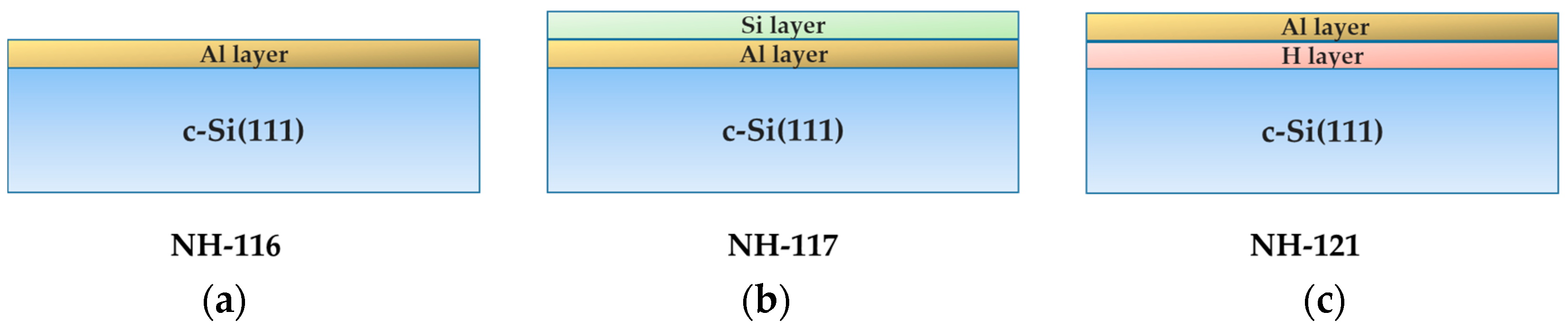
2.1. Sample Preparation
2.2. Sample Characterization
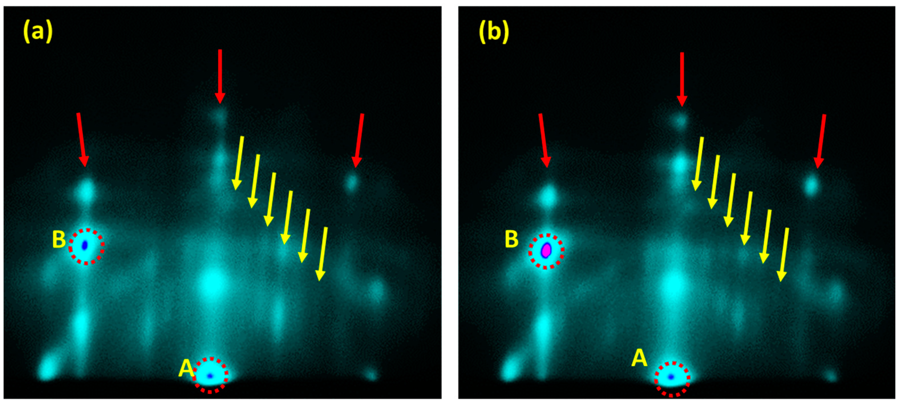
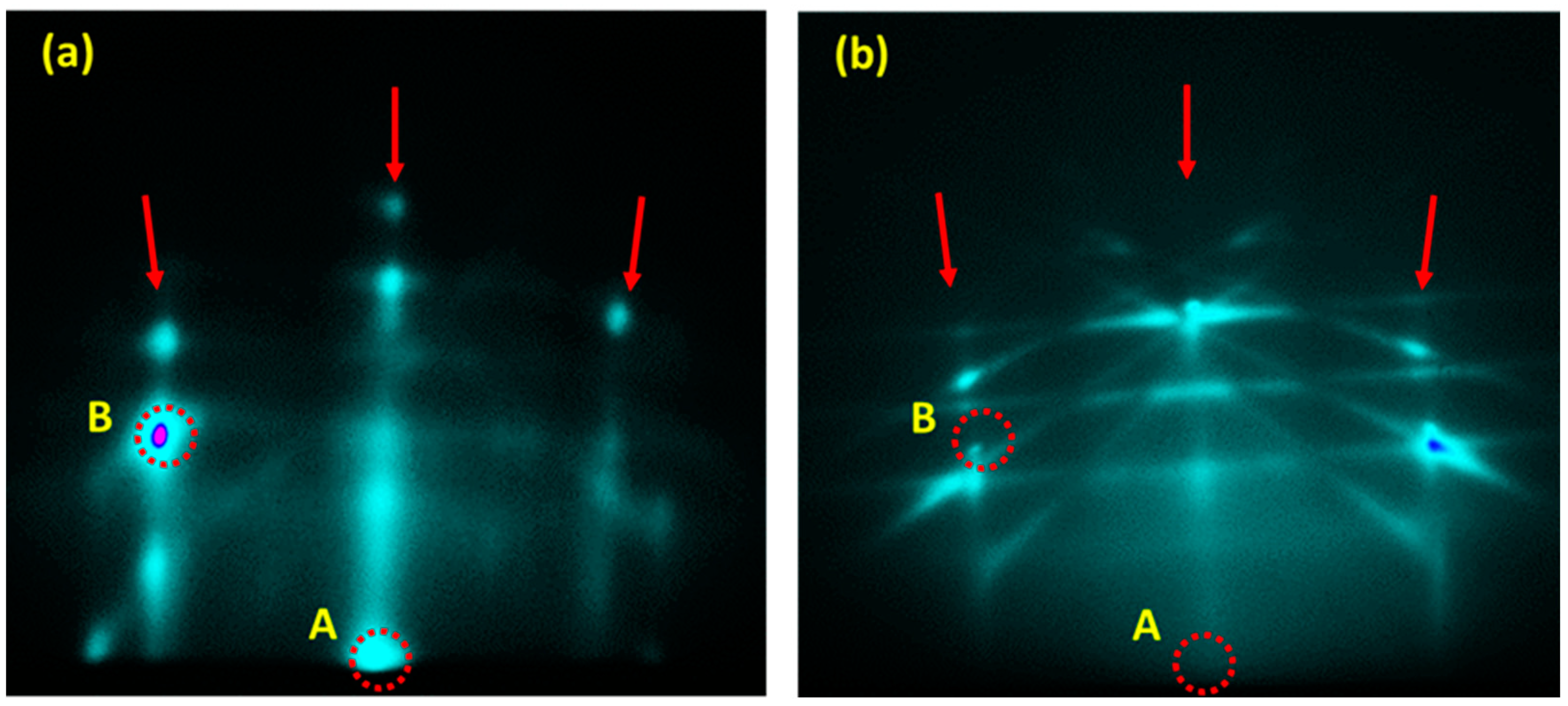
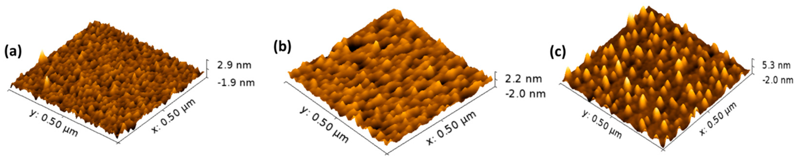
3. Results and Discussion
4. Conclusions
Author Contributions
Funding
Data Availability Statement
Acknowledgments
Conflicts of Interest
References
- Raja, S.S.; Cheng, C.-W.; Sang, Y.; Chen, C.-A.; Zhang, X.-Q.; Dubey, A.; Yen, T.-J.; Chang, Y.-M.; Lee, Y.-H.; Gwo, S. Epitaxial Aluminum Surface-Enhanced Raman Spectroscopy Substrates for Large-Scale 2D Material Characterization. ACS Nano 2020, 14, 8838–8845. [Google Scholar] [CrossRef] [PubMed]
- Derivaz, M.; Dentel, D.; Stephan, R.; Hanf, M.-C.; Mehdaoui, A.; Sonnet, P.; Pirri, C. Continuous Germanene Layer on Al (111). Nano Lett. 2015, 15, 2510–2516. [Google Scholar] [CrossRef] [PubMed]
- Liu, G.; Liu, S.B.; Xu, B.; Ouyang, C.Y.; Song, H.Y.; Guan, S.; Yang, S.A. Multiple Dirac Points and Hydrogenation-Induced Magnetism of Germanene Layer on Al (111) Surface. J. Phys. Chem. Lett. 2015, 6, 4936–4942. [Google Scholar] [CrossRef] [PubMed]
- Morishita, T.; Spencer, M.J.S.; Kawamoto, S.; Snook, I.K. A New Surface and Structure for Silicene: Polygonal Silicene Formation on the Al (111) Surface. J. Phys. Chem. C 2013, 117, 22142–22148. [Google Scholar] [CrossRef]
- Sassa, Y.; Johansson, F.O.; Lindblad, A.; Yazdi, M.G.; Simonov, K.; Weissenrieder, J.; Muntwiler, M.; Iyikanat, F.; Sahin, H.; Angot, T.; et al. Kagome-like silicene: A novel exotic form of two-dimensional epitaxial silicon. Appl. Surf. Sci. 2020, 530, 147195. [Google Scholar] [CrossRef]
- Bakulin, A.V.; Chumakova, L.S.; Korchuganov, A.V.; Kulkova, S.E. Role of Oxygen and Fluorine in Passivation of the GaSb (111) Surface Depending on Its Termination. Crystals 2022, 12, 477. [Google Scholar] [CrossRef]
- Sanna, S.; Plaickner, J.; Holtgrewe, K.; Wettig, V.; Speiser, E.; Chandola, S.; Esser, N. Spectroscopic Analysis of Rare-Earth Silicide Structures on the Si (111) Surface. Materials 2021, 14, 4104. [Google Scholar] [CrossRef]
- Goswami, R.; Qadri, S.; Nepal, N.; Eddy, C., Jr. Microstructure and Interfaces of Ultra-Thin Epitaxial AlN Films Grown by Plasma-Enhanced Atomic Layer Deposition at Relatively Low Temperatures. Coatings 2021, 11, 482. [Google Scholar] [CrossRef]
- Li, W.; Wang, J.; Ding, W.; Gong, Y.; Chen, H.; Ju, D. Exploring the Dual Characteristics of CH3OH Adsorption to Metal Atomic Structures on Si (111)-7 × 7 Surface. Molecules 2021, 26, 5824. [Google Scholar] [CrossRef]
- Lee, T.; Kim, J.; Park, C.; Kim, H.; Kim, M.; Park, H.; Kim, I.; Ko, J.; Pak, K.; Choi, S.Q.; et al. Large-Area Synthesis of Ultrathin, Flexible, and Transparent Conductive Metal–Organic Framework Thin Films via a Microfluidic-Based Solution Shearing Process. Adv. Mater. 2022, 34, 2107696. [Google Scholar] [CrossRef]
- Kumar, S.; Joshi, K.L.; Van Duin, A.C.T.; Haque, M.A. Can amorphization take place in nanoscale interconnects? Nanotechnology 2012, 23, 095701. [Google Scholar] [CrossRef] [PubMed]
- Kumar, S.; Garcia, D.; Jin, J.; Haque, A. Mechanical strain mediated carrier scattering and its role in charge and thermal transport in freestanding nanocrystalline aluminum thin films. J. Vac. Sci. Technol. B Nanotechnol. Microelectron. Mater. Process. Meas. Phenom. 2015, 33, 022002. [Google Scholar] [CrossRef]
- Battaglia, C.; Cuevas, A.; De Wolf, S. High-efficiency crystalline silicon solar cells: Status and perspectives. Energy Environ. Sci. 2016, 9, 1552–1576. [Google Scholar] [CrossRef]
- Bivour, M.; Reichel, C.; Hermle, M.; Glunz, S.W. Improving the a-Si:H(p) rear emitter contact of n-type silicon solar cells. Sol. Energy Mater. Sol. Cells 2012, 106, 11–16. [Google Scholar] [CrossRef]
- Zhang, X.; Chabal, Y.J.; Christman, S.B.; Chaban, E.E.; Garfunkel, E. Oxidation of H-covered flat and vicinal Si (111)-1 × 1 surfaces. J. Vac. Sci. Technol. A Vac. Surf. Film. 2001, 19, 1725–1729. [Google Scholar] [CrossRef]
- Ye, S.; Ichihara, T.; Uosaki, K. Spectroscopic Studies on Electroless Deposition of Copper on a Hydrogen-Terminated Si (111) Surface in Fluoride Solutions. J. Electrochem. Soc. 2001, 148, C421–C426. [Google Scholar] [CrossRef]
- Saranin, A.; Lifshits, V.; Ignatovich, K.; Bethge, H.; Kayser, R.; Goldbach, H.; Klust, A.; Wollschläger, J.; Henzler, M. Restructuring process of the Si (111) surface upon Ca deposition. Surf. Sci. 2000, 448, 87–92. [Google Scholar] [CrossRef]
- Shibata, A.; Kimura, Y.; Takayanagi, K. In situ high-temperature STM study of the restructuring process on the Si(111)7 × 7 surface upon Ag deposition. Surf. Sci. 1994, 303, 161–170. [Google Scholar] [CrossRef]
- Liu, H.; Zhang, Y.; Wang, D.; Pan, M.; Jia, J.; Xue, Q. Two-dimensional growth of Al films on Si (111)-7 × 7 at low-temperature. Surf. Sci. 2004, 571, 5–11. [Google Scholar] [CrossRef]
- Piot, L.; Le Floch, S.; Cornier, T.; Daniele, S.; Machon, D. Amorphization in Nanoparticles. J. Phys. Chem. C 2013, 117, 11133–11140. [Google Scholar] [CrossRef]
- Yeh, C.-W.; Chen, G.-H.; Ho, S.-J.; Chen, H.-S. Inhibiting the Surface Oxidation of Low-Cadmim-Content ZnS:(Cd,Se) Quantum Dots for Enhancing Application Reliability. ACS Appl. Nano Mater. 2019, 2, 5290–5301. [Google Scholar] [CrossRef]
- Kern, W. Overview and evolution of silicon wafer cleaning technology. In Handbook of Silicon Wafer Cleaning Technology; Elsevier: Amsterdam, The Netherlands, 2018; pp. 3–85. [Google Scholar]
- Kern, W. Cleaning solution based on hydrogen peroxide for use in silicon semiconductor technology. RCA Rev. 1970, 31, 187–206. [Google Scholar]
- Machine, W. RCA Clean. Materials at Colorado School of Mines. Available online: https://inside.mines.edu/fs_home/cwolden/Wolden_Webpages/index.html (accessed on 1 January 2019).
- Latyshev, A.; Krasilnikov, A.; Aseev, A.; Sokolov, L.; Stenin, S. Reflection electron microscopy study of clean Si (111) surface reconstruction during the (7 × 7) ς (1 × 1) phase transition. Surf. Sci. 1991, 254, 90–96. [Google Scholar] [CrossRef]
- Takayanagi, K.; Tanishiro, Y.; Takahashi, M. Structural analysis of Si (111)-7 × 7 by UHV-transmission electron diffraction and microscopy. J. Vac. Sci. Technol. A Vac. Surf. Film. 1985, 3, 1502–1506. [Google Scholar] [CrossRef]
- Jiang, Y.; Kim, Y.-H.; Zhang, S.B.; Ebert, P.; Yang, S.; Tang, Z.; Wu, K.; Wang, E.G. Growing extremely thin bulklike metal film on a semiconductor surface: Monolayer Al (111) on Si (111). Appl. Phys. Lett. 2007, 91, 181902. [Google Scholar] [CrossRef]
- Northrup, J.E. Si (111)3 × 3-Al: An Adatom-Induced Reconstruction. Phys. Rev. Lett. 1984, 53, 683–686. [Google Scholar] [CrossRef]
- Uhrberg, R.I.G.; Hansson, G.V.; Nicholls, J.M.; Persson, P.E.S.; Flodström, S.A. Photoemission study of the surface and bulk electronic structures of Si (111) 7 × 7 and Si (111) ≤3¯ × ≤3¯: Al. Phys. Rev. B 1985, 31, 3805–3810. [Google Scholar] [CrossRef]
- Jiang, Y.; Wu, K.; Tang, Z.; Ebert, P.; Wang, E.G. Quantum size effect induced dilute atomic layers in ultrathin Al films. Phys. Rev. B 2007, 76, 035409. [Google Scholar] [CrossRef]
- Ji, H.; Lin, Y.-C.; Nagashio, K.; Maruyama, M.; Solís-Fernández, P.; Aji, A.S.; Panchal, V.; Okada, S.; Suenaga, K.; Ago, H. Hydrogen-Assisted Epitaxial Growth of Monolayer Tungsten Disulfide and Seamless Grain Stitching. Chem. Mater. 2018, 30, 403–411. [Google Scholar] [CrossRef]
- Grant, J.T. AES: Basic principles, spectral features and qualitative analysis. In Surface Analysis by Auger and X-ray Photoelectron Spectroscopy; IM Publications: Amsterdam, The Netherlands, 2003; pp. 57–88. [Google Scholar]
- Moulder, J.F.; Stickle, W.F.; Sobol, P.E.; Bomben, K.D.; Chastian, J. X-ray photoelectron spectroscopy. In Handbook of X-ray Photoelectron Spectroscopy; Perkin-Elmer Corp.: Eden Prairie, MN, USA, 1992. [Google Scholar]
- Wagner, C.D.; Naumkin, A.V.; Kraut-Vass, A.; Allison, J.W.; Powell, C.J.; Rumble, J.R. NIST Standard Reference Database 20, Version 3.4 (Web Version); National Institute of Standards and Technology: Gaithersburg, MD, USA, 2003; p. 20899.
- Nist, X. Ray Photoelectron Spectroscopy Database. Default. aspx, 2015. Available online: http://srdata.nist.gov/xps (accessed on 2 February 2019).
- Nakanishi, S.; Horiguchi, T. Surface Lattice Constants of Si (111), Ni (111) and Cu (111). Jpn. J. Appl. Phys. 1981, 20, L214. [Google Scholar] [CrossRef]
- Yin, C.; Negreiros, F.R.; Barcaro, G.; Beniya, A.; Sementa, L.; Tyo, E.C.; Bartling, S.; Meiwes-Broer, K.-H.; Seifert, S.; Hirata, H.; et al. Alumina-supported sub-nanometer Pt10 clusters: Amorphization and role of the support material in a highly active CO oxidation catalyst. J. Mater. Chem. A 2017, 5, 4923–4931. [Google Scholar] [CrossRef]
- Olafsen, J.S.; Urbach, J.S. Clustering, Order, and Collapse in a Driven Granular Monolayer. Phys. Rev. Lett. 1998, 81, 4369–4372. [Google Scholar] [CrossRef]
- Huanca, D.R. Aluminum modified silicon surfaces: Optical and electrical characterization. Appl. Surf. Sci. 2021, 565, 150496. [Google Scholar] [CrossRef]
- Noh, J.-S. Aluminum silicide microparticles transformed from aluminum thin films by hypoeutectic interdiffusion. Nanoscale Res. Lett. 2014, 9, 312. [Google Scholar] [CrossRef] [PubMed]
- Wu, H.; Zheng, L.; Zhan, J.; Du, N.; Liu, W.; Ma, J.; Su, L.; Wang, L. Recycling silicon-based industrial waste as sustainable sources of Si/SiO2 composites for high-performance Li-ion battery anodes. J. Power Sources 2020, 449, 227513. [Google Scholar] [CrossRef]
- Sun, C.; Zeng, R.; Zhang, J.; Qiu, Z.-J.; Wu, D. Effects of UV-Ozone Treatment on Sensing Behaviours of EGFETs with Al2O3 Sensing Film. Materials 2017, 10, 1432. [Google Scholar] [CrossRef]
- Lin, K.-Y.; Li, C.; Engelmann, S.; Bruce, R.L.; Joseph, E.A.; Metzler, D.; Oehrlein, G.S. Achieving ultrahigh etching selectivity of SiO2 over Si3N4 and Si in atomic layer etching by exploiting chemistry of complex hydrofluorocarbon precursors. J. Vac. Sci. Technol. A Vac. Surf. Film. 2018, 36, 040601. [Google Scholar] [CrossRef]
- Dvoretckaia, L.; Gridchin, V.; Mozharov, A.; Maksimova, A.; Dragunova, A.; Melnichenko, I.; Mitin, D.; Vinogradov, A.; Mukhin, I.; Cirlin, G. Light-Emitting Diodes Based on InGaN/GaN Nanowires on Microsphere-Lithography-Patterned Si Substrates. Nanomaterials 2022, 12, 1993. [Google Scholar] [CrossRef]
- Deng, S.; Xu, R.; Seh, W.; Sun, J.; Cai, W.; Zou, J.; Zhang, Q. Current degradation mechanism of tip contact metal-silicon Schottky nanogenerator. Nano Energy 2022, 94, 10688. [Google Scholar] [CrossRef]


| Take-Off Angle | ||||||
|---|---|---|---|---|---|---|
| NH-116 | NH-117 | NH-121 | ||||
| Element | 0° | 45° | 0° | 45° | 0° | 45° |
| Si | 37.6 | 30.3 | 38.3 | 31.3 | 39.5 | 28.3 |
| Al | 3.6 | 2.1 | 1.6 | 2.1 | 1.3 | 1.2 |
| O | 27.2 | 27.0 | 31.7 | 35.7 | 21.2 | 20.4 |
| C | 31.6 | 40.6 | 28.4 | 30.9 | 32.4 | 42.8 |
| F | - | - | - | - | 5.6 | 7.3 |
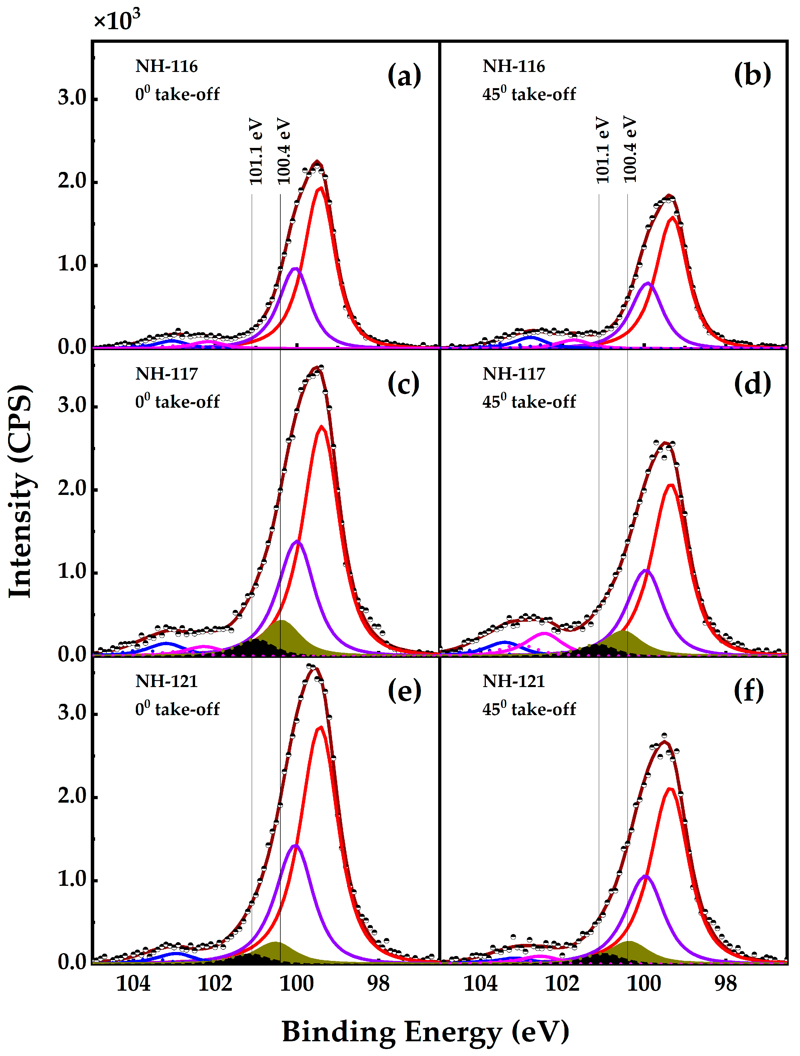
| Si Species | Peak Position (eV) | Assignment | ||
|---|---|---|---|---|
| NH-116 | NH-117 | NH-121 | ||
| #1 | 99.4 | 99.4 | 99.4 | Elemental Silicon |
| 100.0 | 100.0 | 100.0 | ||
| #2 | 102.9 | 103.1 | 103.1 | SiO2 or AlxSiyOz |
| 103.5 | 103.7 | 103.7 | ||
| #3 | - | 100.4 | 100.4 | AlSi, SiC |
| - | 101.1 | 101.1 | ||
| #4 | 101.9 | 102.5 | 102.5 | SiO or AlxSiyOz |
| 102.6 | 103.2 | 103.2 | ||
| Sample | Peak Position (eV) | Assignment |
|---|---|---|
| NH-116 | 75.5 | Al2O3/Si |
| NH-117 | 75.5 | Al2O3/Si |
| NH-121 | 75.5 | Al2O3/Si |
| C 1s Peak | Peak Position (eV) | Assignment | ||
|---|---|---|---|---|
| NH-116 | NH-117 | NH-121 | ||
| 1 | 285.7 | 285.7 | 285.4 | -CH2C(O)O |
| 2 | 287.5 | 287.3 | 287.2 | -C(O)-, CH3OH/Si |
| 3 | 290.0 | 290.0 | 289.3 | -C(O)O, CO3, CO3 |
| 4 | 283.5 | 283.6 | SiC | |
| 5 | 292.0 | -CF8 | ||
| MSE | Thickness (nm) | Voids % | Al% | SiO2% | Al2O3% | |
|---|---|---|---|---|---|---|
| NH-116 | 2.87 | 2.70 | 43.2 | 4.9 | 26.8 | 25.1 |
| NH-117 | 2.88 | 2.73 | 42.2 | 5.4 | 26.6 | 25.8 |
| NH-121 | 2.43 | 3.38 | 25.2 | 0.5 | 29.3 | 45.0 |
Disclaimer/Publisher’s Note: The statements, opinions and data contained in all publications are solely those of the individual author(s) and contributor(s) and not of MDPI and/or the editor(s). MDPI and/or the editor(s) disclaim responsibility for any injury to people or property resulting from any ideas, methods, instructions or products referred to in the content. |
© 2023 by the authors. Licensee MDPI, Basel, Switzerland. This article is an open access article distributed under the terms and conditions of the Creative Commons Attribution (CC BY) license (https://creativecommons.org/licenses/by/4.0/).
Share and Cite
Jum’h, I.; Abu-Safe, H.H.; Ware, M.E.; Qattan, I.A.; Telfah, A.; Tavares, C.J. Surface Atomic Arrangement of Aluminum Ultra-Thin Layers Grown on Si(111). Nanomaterials 2023, 13, 970. https://doi.org/10.3390/nano13060970
Jum’h I, Abu-Safe HH, Ware ME, Qattan IA, Telfah A, Tavares CJ. Surface Atomic Arrangement of Aluminum Ultra-Thin Layers Grown on Si(111). Nanomaterials. 2023; 13(6):970. https://doi.org/10.3390/nano13060970
Chicago/Turabian StyleJum’h, Inshad, Husam H. Abu-Safe, Morgan E. Ware, I. A. Qattan, Ahmad Telfah, and Carlos J. Tavares. 2023. "Surface Atomic Arrangement of Aluminum Ultra-Thin Layers Grown on Si(111)" Nanomaterials 13, no. 6: 970. https://doi.org/10.3390/nano13060970
APA StyleJum’h, I., Abu-Safe, H. H., Ware, M. E., Qattan, I. A., Telfah, A., & Tavares, C. J. (2023). Surface Atomic Arrangement of Aluminum Ultra-Thin Layers Grown on Si(111). Nanomaterials, 13(6), 970. https://doi.org/10.3390/nano13060970