Communication

Great Potential of Si-Te Ovonic Threshold Selector in Electrical Performance and Scalability

1
State Key Laboratory of Functional Materials for Informatics, Shanghai Institute of Micro-System and Information Technology, Chinese Academy of Sciences, Shanghai 200050, China
2
University of Chinese Academy of Sciences, Beijing 100029, China
*
Authors to whom correspondence should be addressed.
Nanomaterials 2023, 13(6), 1114; https://doi.org/10.3390/nano13061114
Submission received: 2 March 2023 / Revised: 16 March 2023 / Accepted: 17 March 2023 / Published: 21 March 2023

Abstract

:
The selector is an indispensable section of the phase change memory (PCM) chip, where it not only suppresses the crosstalk, but also provides high on-current to melt the incorporated phase change material. In fact, the ovonic threshold switching (OTS) selector is utilized in 3D stacking PCM chips by virtue of its high scalability and driving capability. In this paper, the influence of Si concentration on the electrical properties of Si-Te OTS materials is studied; the threshold voltage and leakage current remain basically unchanged with the decrease in electrode diameter. Meanwhile, the on-current density (Jon) increases significantly as the device is scaling down, and 25 MA/cm2 on-current density is achieved in the 60-nm SiTe device. In addition, we also determine the state of the Si-Te OTS layer and preliminarily obtain the approximate band structure, from which we infer that the conduction mechanism conforms to the Poole-Frenkel (PF) model.

1. Introduction

The fact that the digital data are exponentially increasing at every moment has put forward a series of higher requirements for memory—more reliability with less cost, greater memory capacity with smaller sizes, and faster read/write speed with lower power consumption [1,2]. Compared to NAND Flash devices, PCM has been one of the most promising competitors of the next-generation memories on the strength of structural transition of chalcogenides between crystalline and amorphous states [3,4] which has shown extraordinary advantages in operating speed, storage density and endurance [5]. Moreover, the successful commercialization of PCM [6] is also inseparable from the help of ovonic threshold switching (OTS), which tends to suppress leakage current in case of operating errors. Compared with traditional Si-based switches, OTS materials acting as just nm-scale films dispense with the share of Si substrate and possess highly potential in scalability [7].
However, loads of materials with superior performance emerging from the OTS research in full swing contain eco-unfriendly elements such as sulfur [8,9,10], arsenic [11,12] etc.; additionally, most OTS materials are ternary, quaternary or even more [13,14], which means they inevitably suffer from element segregation and inhomogeneous composition. At the same time, OTS switches are required to maintain an amorphous state at the high temperature of 400–450 °C, which is also called back-end-of-line (BEOL) process [1,15], posing a serious challenge to binary Se- and Te-based materials [16,17]. In 2021, a major breakthrough was made by Shen et al., in that tellurium was discovered to be the simplest threshold switching material with an endurance of 108 cycles. The selectivity is higher than 103 and the on current density is more than 11 MA/cm2, which is enough to drive the incorporated PCM. Different from previous OTS materials, the Te layer stays in a crystalline state before and after pulse operation; therefore, Shen et al. creatively raised a brand-new principle called the ‘Crystalline-Liquid-Crystalline Mechanism’, which corresponds the off state of the switch to the crystalline state of Te and then Te melts into liquid under the external voltage, which means the switch turns on. At the removal of applied voltage, Te rapidly recrystallizes and the device turns off. In addition, the single element also avoids the limitations from the high temperature of the BEOL process and the element/phase segregation [1].
Unluckily, the leakage current at 1/2 Vth, i.e., Ioff, of 60 nm Te device is only 0.5 μA according to Shen’s research, which indicates the subthreshold region of Te is composed of two parts; one is dominated by the Schottky barrier between Te and TiN electrodes in low electric field, and the other depends on the intrinsic excitation of Te in higher field. Therefore, the ways to optimize the Ioff lie in two perspectives: one is to increase the Schottky barrier by changing the electrode material, such as Pt; the other is to increase the band gap of the material including Si [18,19,20] or B [21] doping.
In our work, we carry out electrical tests on SiTe-based devices to explore the influence of different Si contents on device performance and their potential to scale down. Then we study the conduction mechanism of SiTe devices through characterization.

2. Materials and Methods

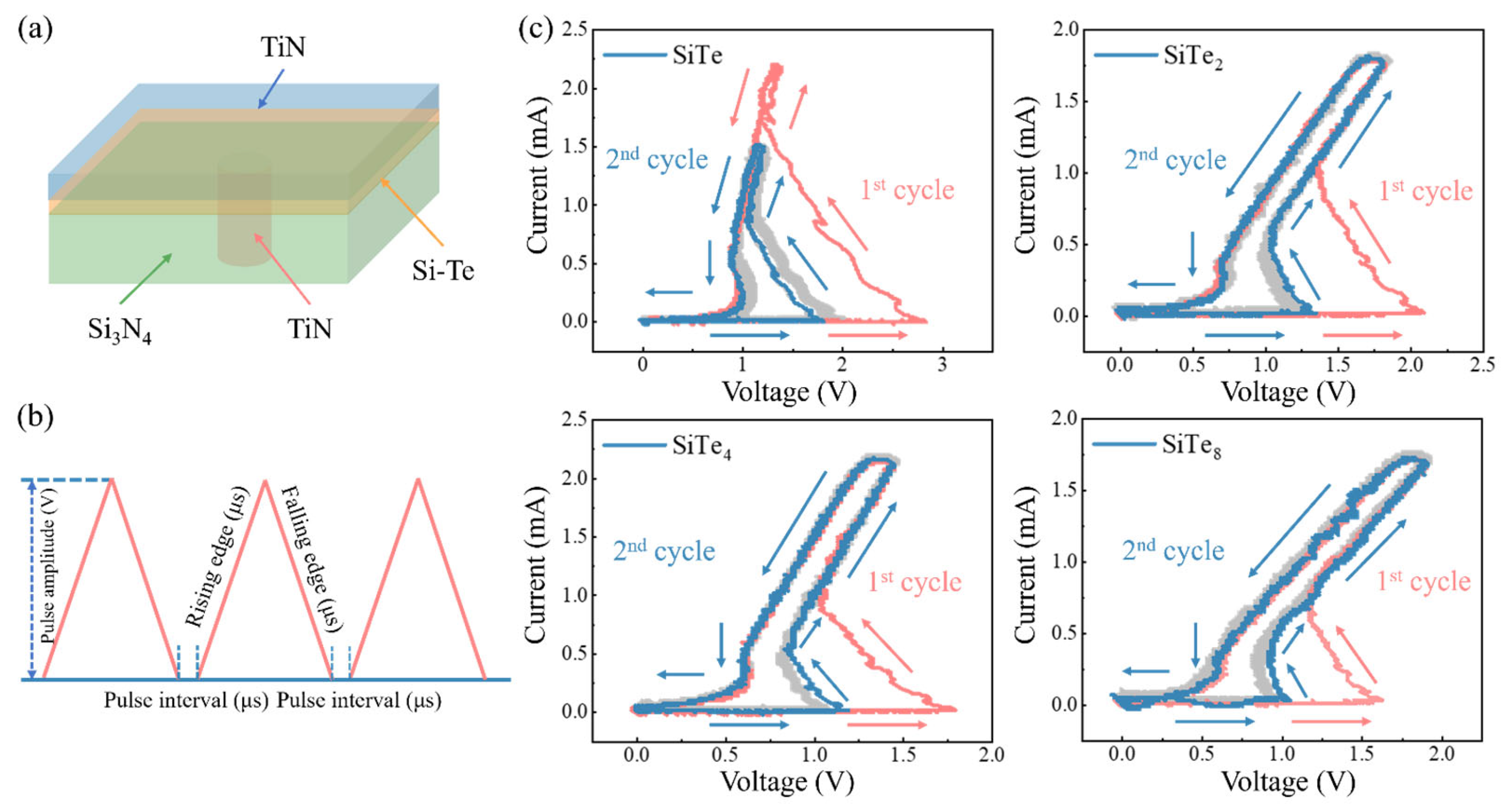
2.1. Film Preparation and Testing

Four compositions are designed to be SiTe, SiTe2, SiTe4 and SiTe8. All the films were deposited by co-sputtering of Si and Te targets, while the power values of Si target are 65 W, 40 W, 30 W and 20 W with 10 W of Te target. The exact components were determined by energy-dispersive spectroscopy (EDS). 100 nm-thick films were deposited on SiO2 substrates for in situ resistance-temperature (R-T) tests with 20 °C/min heating rate and X-ray diffraction (XRD) tests ranging from 10–67°. The Fermi level of different films were measured by X-ray photoelectron spectroscopy (XPS), and 400-nm Si-Te films were deposited on quartz glass as the ultraviolet-visible Spectrophotometer (UV-Vis) samples.

2.2. Device Fabrication

The 10 nm Si-Te OTS layers were deposited on TiN bottom electrodes whose diameters are 200, 150, 120 and 60 nm, respectively. Then, TiN was sputtered as the top electrode with 40-nm thickness. Keithley 4200A-SCS parameter analyzer was used to measure the electrical performance. Tektronix MSO54 mixed signal oscilloscope was used to capture the input pulses and device responses.

3. Results

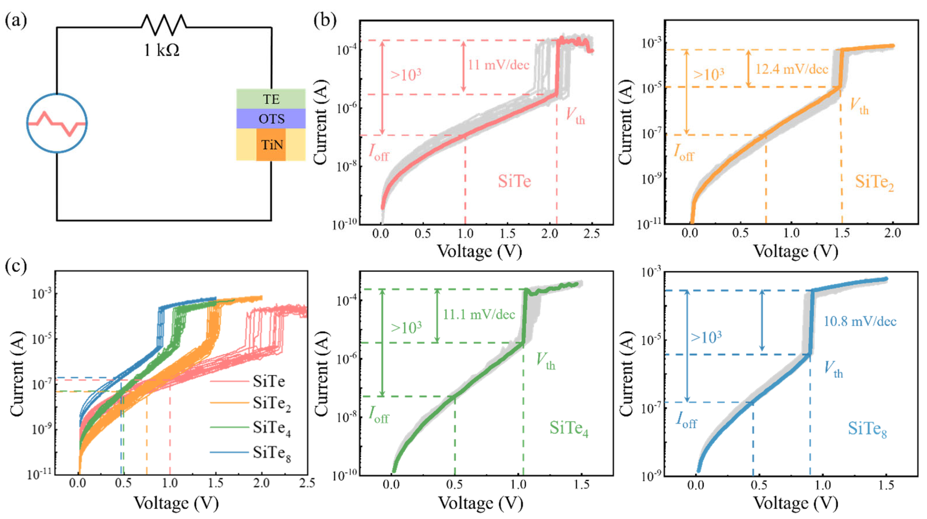
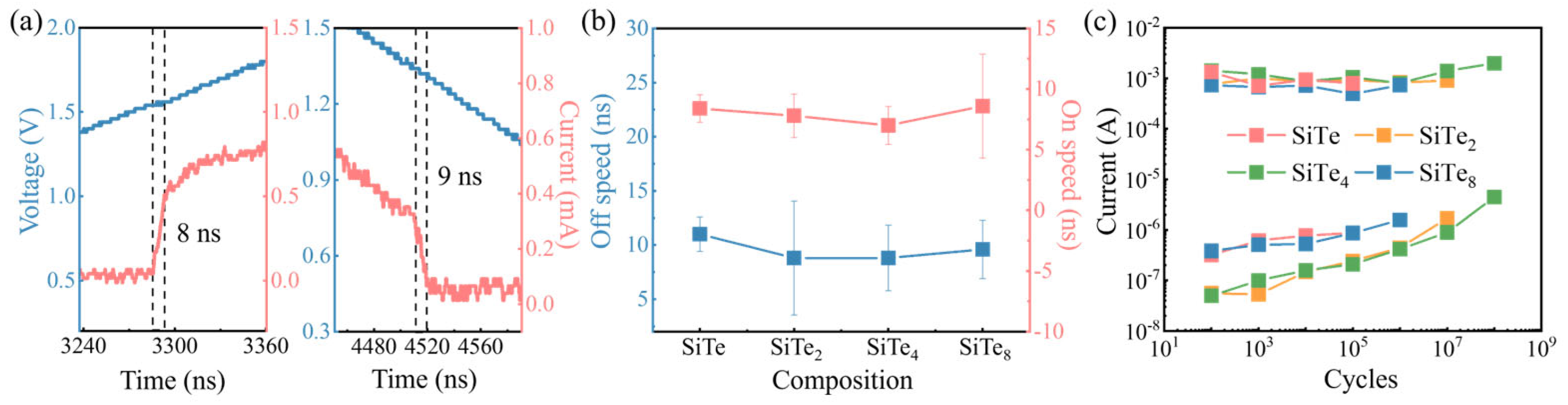
3.1. Variations of Electrical Performance with Different Si Concentrations

T-shaped device structure is shown in Figure 1a where cylindrical TiN serves as the bottom electrode and Si3N4 acts as the isolation. Then current-voltage (I-V) curves of 200 nm-electrode devices with all four Si-Te compositions under 10 continuous triangular pulses (Figure 1b) are shown in Figure 1c. The red lines represent the response of device under the first pulse, which is called first fire (FF). During the process, SiTe device suddenly turns to low resistance state at 2.83 V, while under the second pulse, the threshold voltage (Vth) goes down to 1.71 V as described by the blue lines. With the decrease of Si content, the fire voltage (Vfire) of SiTe2 drops to 2.09 V. After FF process, only 1.11–1.31 V Vth is needed to operate the cell. The downward trend continues with SiTe4 and SiTe8, whose Vfire were 1.79 V and 1.63 V, respectively. Moreover, Vth of SiTe4 is ~0.8 V lower than its Vfire which fluctuates between 0.99 and 1.13 V, while the Vth of SiTe8 ranges from 0.89 V to 1.05 V. The amplitude of the first pulse applied to the SiTe device is 4 V and the height of the remaining nine pulses is 3 V. Meanwhile, the pulse amplitude of all ten triangular pulses used for other Si-Te devices is 4 V. The rising edges, falling edges and pulse intervals of these pulses are 1 μs. Clearly, both Vfire and Vth keep decreasing with the continuous decrease of Si contents.
Afterwards, we carried out DC I-V tests and the circuit is shown in Figure 2a. From Figure 2b, we can obviously find that the change trend of Vth is consistent with the results of pulsed I-V, that is, the addition of silicon will lead to the rise of Vth. As can be seen in the figure, all Si-Te devices show >10 mV/dec nonlinear characteristics and more than 103 selective ratio. In addition, the leakage current of SiTe at ~1/2 Vth, namely Ioff, which is about 0.12 μA, and the Ioff of SiTe2 is situated at ~93 nA. It continued to decrease to 53 nA by the concentration of Si declines to 20 at. %, but contrary to the down trend of Si concentration, Ioff increases to 0.15 μA in SiTe8. However, after summarizing and comparing the DC curves of the four components as shown in Figure 2c, we clearly observed that - the leakage current decreases with the increase of Si content.
Other electrical performances are shown in Figure 3. Instantaneous responses of the device are observed through the oscilloscope, from which we are able to capture the moment when the device is turned on and off, as shown in Figure 3a. The abrupt rise of current signifies that the device is switched on, while the time span is considered to be the on-speed. Similarly, a sudden drop in current refers to the off-speed. As shown in Figure 3b, the content of silicon seems independent of the switching speeds. Moreover, the lifetime of the devices was measured with the help of the oscilloscope. A fixed number of continuous pulses is applied to the device, and whether the device still works normally is judged from the screen. In case the device responds to each pulse, a DC test is conducted next to measure its Ioff in order to verify whether the off-state is in a high-resistance state as before. Only if both conditions are met, the endurance with that fixed number is proved. Then the number of input pulses gradually increases until the device keeps silent to the input or the Ioff of the device goes too large. In this way, we find the endurance of both SiTe and SiTe8 are merely 105, but the reason for that low value is slightly different. SiTe is unable to be switched on after 105 pulses. As for SiTe8, it could be turned on but its Ioff is too large, which may be due to the low crystallization temperature. As shown in Figure 3c, SiTe2 device enables to operate for 108 cycles which shows the longest lifetime among these four contents.

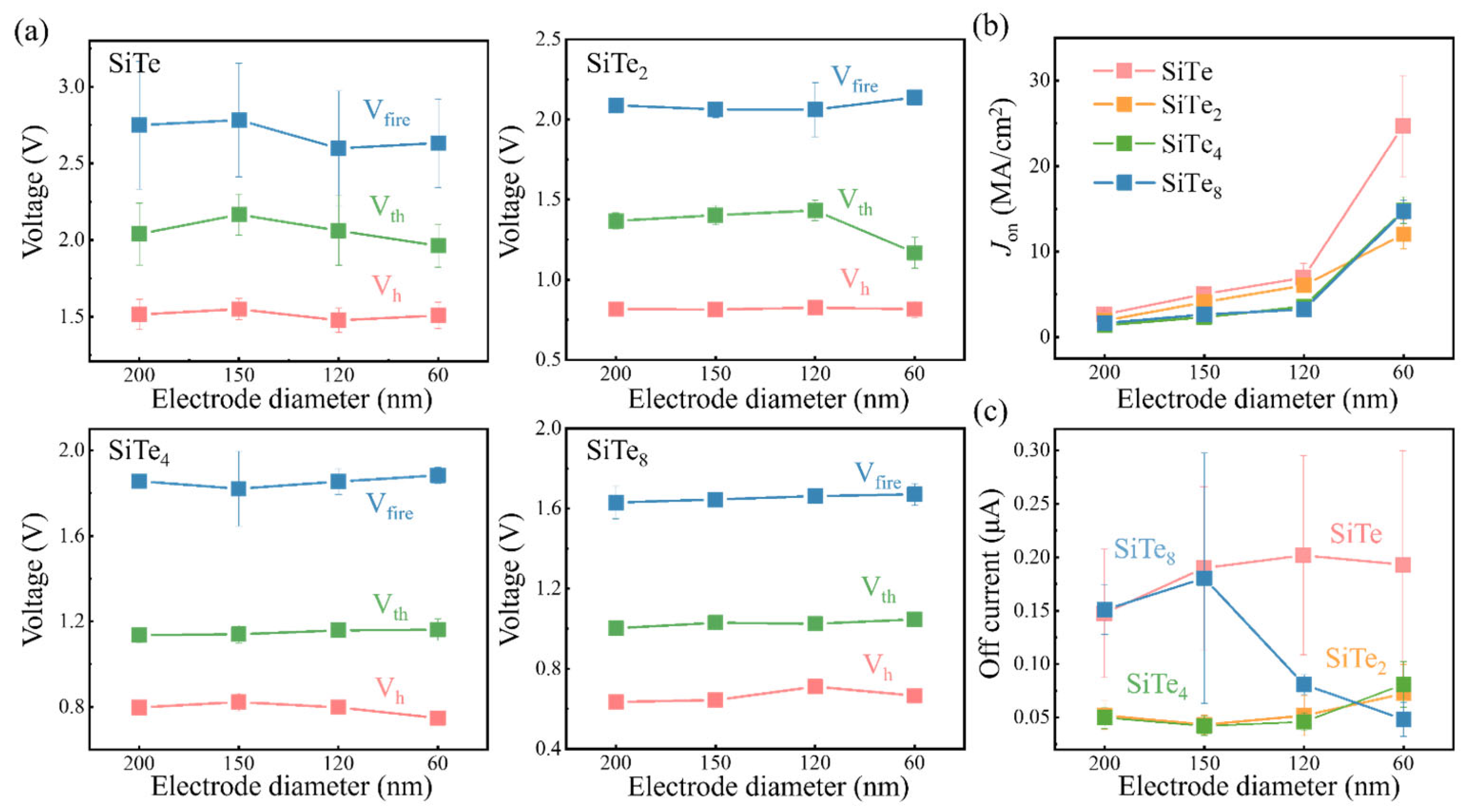
3.2. Effect of Device Size on Electrical Performance

From the perspective of market demand, device shrinkage has been focused, and whether the device maintains the performance with scaling down has been a major problem. First, we explored the relationships between Vfire, Vth, holding voltage (Vh) and electrode sizes. In fact, Vfire significantly affects the device lifetime and power consumption, while Vth and Vh are directly related to the read margin [22], that is, a slight shift of Vth or Vh may cause serious operation errors. Luckily, Si-Te series devices show high potential in scalability from Figure 4a. According to the statistics of more than 50 independent cells, Vfire, Vth and Vh are almost irrelevant to the device size. Clearly shown in Figure 4a and Figure 1c, the read margin becomes narrow with the decrease of Si content, but the good news is that Vfire also becomes smaller. Therefore, the key to application is how to balance these two points. In addition, the reduction of device size brings the increase of on-current density as well. Generally, >10 MA/cm2 is required to drive the PCM. From Figure 4b, the on-current density of 60 nm-SiTe device reaches 25 MA/cm2 at most, and Jon of the other components also exceed 10 MA/cm2. As for Ioff, it hardly changes with the electrode size according to Figure 4c. The discrepancy of SiTe8 results from the number of devices participating in statistics. Under comprehensive consideration, SiTe2 is equipped with >15 mA/cm2 on-current density, 108 cycles of endurance, and moderate Ioff among these compositions, which is the best choice of the four components.

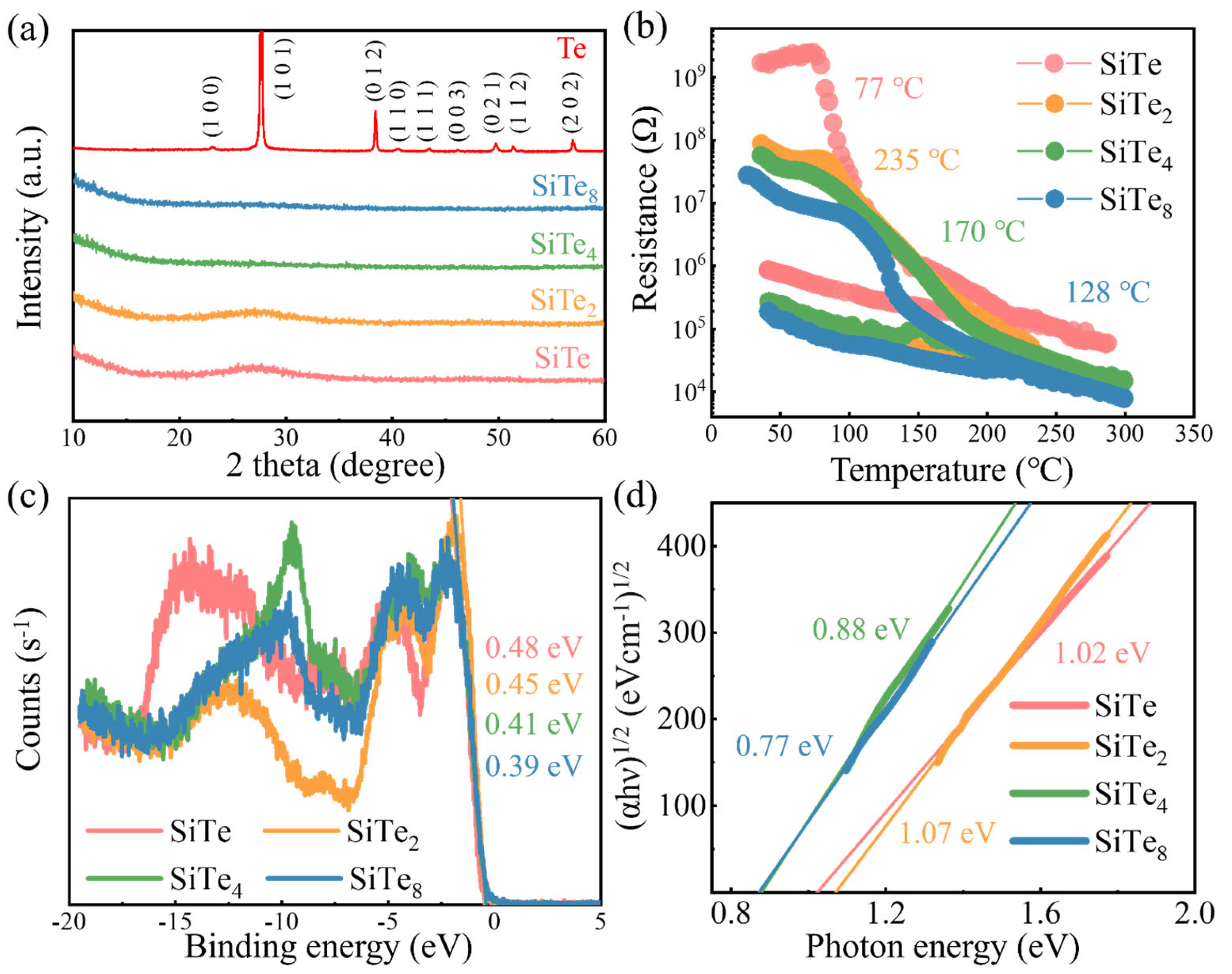
3.3. Characterization of Si-Te Films

We first carried out XRD tests on the as-deposited films of each component, as shown in Figure 5a. As seen from the figure, Si-Te films of the four components show no peak, but there are obvious crystallization peaks in the Te sample, indicating that the deposited Te is in crystalline state, while the state of film turns to amorphous after Si incorporation. At the same time, the state of the material has also been proved by R-T test in Figure 5b. Interestingly, the crystallization temperature of SiTe is only 78 °C, and the crystallization temperature reaches the peak of ~235 °C at SiTe2. However, with the further reduction of Si content, the crystallization temperature decreases, and that of SiTe8 decreases to 128 °C, the tendency which is very similar to Ge-Te system [23]. Moreover, the different states directly indicate that the conduction mechanism of Si-Te is different from that of Te, while the Si-Te device is more consistent with the traditional PF model [24], where the switching characteristic strongly depends on the amorphous state. Then the location of the valence band maximums (VBM, Ev) are determined by linear extrapolation of the linear part of the XPS valence band spectrum, they are situated at −0.48 eV, −0.45 eV, −0.41 eV and −0.39 eV for SiTe, SiTe2, SiTe4 and SiTe8, respectively, in Figure 5c. Meanwhile, the band gap is obtained by linear fitting according to αhν = C (hν − Eg)2, where C is the constant, and α is the absorption coefficient, as shown in Figure 5d. The band gap value of SiTe is 1.02 eV. With the decrease of Si concentration, the band gap slightly increases to 1.07 eV, and further drops to 0.88 eV and 0.87 eV for SiTe4 and SiTe8. The Fermi level is basically located in the center of the band gap, which is generally believed that the high concentration defect states would pin the Fermi level in the middle of the band gap. Si-Te series materials basically conform to this rule, that is to say, their conduction mechanism may be closely related to the defect state, which requires further research.

4. Conclusions

In this paper, we comprehensively studied the relationships between the electrical properties of Si-Te devices and Si concentration. Although the operation speed of the Si-Te device is maintained at ~10 ns, Vfire and Vth gradually rise and Ioff drops as the Si concentration goes up. However, the steady increase of Si concentration also leads to the lifetime degradation when the Si concentration exceeds 33 at. %, where the SiTe2 device exhibits a superior endurance of 108 cycles to other contents. In addition, Vth, Ion and Ioff of all components hardly change with the electrode size, and the Jon of 60-nm SiTe device even increases to 25 MA/cm2, indicating the great potential of Si-Te devices in scaling down. In terms of the conduction mechanism of Si-Te, we firstly find that Si-Te materials are amorphous by XRD, and observe the change in trend whereby the crystallization temperature increases and then decreases with the decrease of Si contents through in situ RT experiment. Through UV-vis, we also find that the root of Ioff variation with Si concentration originates from the band gap, that is, the larger the content of Si, the wider the band gap, and the smaller the Ioff. Afterwards, the Fermi level is found to be pinned at the center of the band gap through XPS, indicating that the conduction mechanism is more consistent with the traditional PF model associated with trap state which is different from Te switching. The specific relationship between the switching performance of Si-Te materials and the defect state is also worthy of further study.

Author Contributions

R.W. deposited the films, prepared the devices, measured device performances and wrote the paper. Y.S., S.Z. and Z.Z. revised the paper. The project was initiated and conceptualized by Z.S. All authors have read and agreed to the published version of the manuscript.

Funding

Financial support was provided by the Strategic Priority Research Program of the Chinese Academy of Sciences (XDB44010200) and the National Natural Science Foundation of China (61904046).

Data Availability Statement

Not applicable.

Acknowledgments

The authors acknowledge the financial support from the State Key Laboratory of Functional Materials for Informatics, Shanghai Institute of Microsystem and Information, Chinese Academy of Sciences.

Conflicts of Interest

The authors declare no conflict of interest.

References

  1. Shen, J.; Jia, S.; Shi, N.; Ge, Q.; Gotoh, T.; Lv, S.; Liu, Q.; Dronskowski, R.; Elliott, S.R.; Song, Z.; et al. Elemental Electrical Switch Enabling Phase Segregation–Free Operation. Science 2021, 374, 1390–1394. [Google Scholar] [CrossRef] [PubMed]
  2. Calarco, R.; Arciprete, F. Keep It Simple and Switch to Pure Tellurium. Science 2021, 374, 1321–1322. [Google Scholar] [CrossRef] [PubMed]
  3. Wuttig, M.; Yamada, N. Phase-Change Materials for Rewriteable Data Storage. Nat. Mater. 2007, 6, 824–832. [Google Scholar] [CrossRef] [PubMed]
  4. Zhu, M.; Song, W.; Konze, P.M.; Li, T.; Gault, B.; Chen, X.; Shen, J.; Lv, S.; Song, Z.; Wuttig, M.; et al. Direct Atomic Insight into the Role of Dopants in Phase-Change Materials. Nat. Commun. 2019, 10, 3525. [Google Scholar] [CrossRef] [PubMed] [Green Version]
  5. Lai, S.; Lowrey, T. OUM—A 180 nm Nonvolatile Memory Cell Element Technology for Stand Alone and Embedded Applications. In Proceedings of the International Electron Devices Meeting. Technical Digest, Washington, DC, USA, 2–5 December 2001; IEEE: Piscataway, NJ, USA, 2001; pp. 36.5.1–36.5.4. [Google Scholar] [CrossRef]
  6. Choe, J. Memory Technology 2021: Trends & Challenges. In Proceedings of the 2021 International Conference on Simulation of Semiconductor Processes and Devices (SISPAD), Dallas, TX, USA, 27–29 September 2021; IEEE: Piscataway, NJ, USA, 2021; pp. 111–115. [Google Scholar] [CrossRef]
  7. Kau, D.; Tang, S.; Karpov, I.V.; Dodge, R.; Klehn, B.; Kalb, J.A.; Strand, J.; Diaz, A.; Leung, N.; Wu, J.; et al. A Stackable Cross Point Phase Change Memory. In Proceedings of the Technical Digest—International Electron Devices Meeting, IEDM, Baltimore, MD, USA, 7–9 December 2009; IEEE: Piscataway, NJ, USA, 2009; pp. 1–4. [Google Scholar] [CrossRef]
  8. Jia, S.; Li, H.; Gotoh, T.; Longeaud, C.; Zhang, B.; Lyu, J.; Lv, S.; Zhu, M.; Song, Z.; Liu, Q.; et al. Ultrahigh Drive Current and Large Selectivity in GeS Selector. Nat. Commun. 2020, 11, 4636. [Google Scholar] [CrossRef] [PubMed]
  9. Wu, R.; Jia, S.; Gotoh, T.; Luo, Q.; Song, Z.; Zhu, M. Screening Switching Materials with Low Leakage Current and High Thermal Stability for Neuromorphic Computing. Adv. Electron. Mater. 2022, 8, 2200150. [Google Scholar] [CrossRef]
  10. Jia, S.; Li, H.; Liu, Q.; Song, Z.; Zhu, M. Scalability of Sulfur-Based Ovonic Threshold Selectors for 3D Stackable Memory Applications. Phys. Status Solidi Rapid Res. Lett. 2021, 15, 2100084. [Google Scholar] [CrossRef]
  11. Yuan, Z.; Li, X.; Song, S.; Song, Z.; Zha, J.; Han, G.; Yang, B.; Jimbo, T.; Suu, K. The Enhanced Performance of a Si–As–Se Ovonic Threshold Switching Selector. J. Mater. Chem. C 2021, 9, 13376–13383. [Google Scholar] [CrossRef]
  12. Yuan, Z.; Li, X.; Wang, H.; Xue, Y.; Song, S.; Song, Z.; Zhu, S.; Han, G.; Yang, B.; Jimbo, T.; et al. Characteristic of As3Se4-Based Ovonic Threshold Switching Device. J. Mater. Sci. Mater. Electron. 2021, 32, 7209–7214. [Google Scholar] [CrossRef]
  13. Cheng, H.Y.; Chien, W.C.; Kuo, I.T.; Lai, E.K.; Zhu, Y.; Jordan-Sweet, J.L.; Ray, A.; Carta, F.; Lee, F.M.; Tseng, P.H.; et al. An Ultra High Endurance and Thermally Stable Selector Based on TeAsGeSiSe Chalcogenides Compatible with BEOL IC Integration for Cross-Point PCM. In Proceedings of the 2017 IEEE International Electron Devices Meeting (IEDM), San Francisco, CA, USA, 2–6 December 2017; IEEE: Piscataway, NJ, USA, 2017; Volume 1, pp. 2.2.1–2.2.4. [Google Scholar] [CrossRef]
  14. Garbin, D.; Devulder, W.; Degraeve, R.; Donadio, G.L.; Clima, S.; Opsomer, K.; Fantini, A.; Cellier, D.; Kim, W.G.; Pakala, M.; et al. Composition Optimization and Device Understanding of Si-Ge-As-Te Ovonic Threshold Switch Selector with Excellent Endurance. In Proceedings of the 2019 IEEE International Electron Devices Meeting (IEDM), San Francisco, CA, USA, 7–11 December 2019; IEEE: Piscataway, NJ, USA, 2019; pp. 35.1.1–35.1.4. [Google Scholar] [CrossRef]
  15. Zhu, M.; Ren, K.; Song, Z. Ovonic Threshold Switching Selectors for Three-Dimensional Stackable Phase-Change Memory. MRS Bull. 2019, 44, 715–720. [Google Scholar] [CrossRef]
  16. Keukelier, J.; Opsomer, K.; Devulder, W.; Clima, S.; Goux, L.; Sankar Kar, G.; Detavernier, C. Tuning of the Thermal Stability and Ovonic Threshold Switching Properties of GeSe with Metallic and Non-Metallic Alloying Elements. J. Appl. Phys. 2021, 130, 165103. [Google Scholar] [CrossRef]
  17. Anbarasu, M.; Wimmer, M.; Bruns, G.; Salinga, M.; Wuttig, M. Nanosecond Threshold Switching of GeTe6 Cells and Their Potential as Selector Devices. Appl. Phys. Lett. 2012, 100, 143505. [Google Scholar] [CrossRef]
  18. Li, X.; Yuan, Z.; Lv, S.; Song, S.; Song, Z. Extended Endurance Performance and Reduced Threshold Voltage by Doping Si in GeSe-Based Ovonic Threshold Switching Selectors. Thin Solid Films 2021, 734, 1–9. [Google Scholar] [CrossRef]
  19. Koo, Y.; Lee, S.; Park, S.; Yang, M.; Hwang, H. Simple Binary Ovonic Threshold Switching Material SiTe and Its Excellent Selector Performance for High-Density Memory Array Application. IEEE Electron Device Lett. 2017, 38, 568–571. [Google Scholar] [CrossRef]
  20. Velea, A.; Opsomer, K.; Devulder, W.; Dumortier, J.; Fan, J.; Detavernier, C.; Jurczak, M.; Govoreanu, B. Te-Based Chalcogenide Materials for Selector Applications. Sci. Rep. 2017, 7, 8103. [Google Scholar] [CrossRef] [PubMed] [Green Version]
  21. Yoo, J.; Lee, D.; Park, J.; Song, J.; Hwang, H. Steep Slope Field-Effect Transistors with B-Te-Based Ovonic Threshold Switch Device. IEEE J. Electron Devices Soc. 2018, 6, 821–824. [Google Scholar] [CrossRef]
  22. Cheng, H.Y.; Chien, W.C.; Kuo, I.T.; Yeh, C.W.; Gignac, L.; Kim, W.; Lai, E.K.; Lin, Y.F.; Bruce, R.L.; Lavoie, C.; et al. Ultra-High Endurance and Low IOFF Selector Based on AsSeGe Chalcogenides for Wide Memory Window 3D Stackable Crosspoint Memory. In Proceedings of the 2018 IEEE International Electron Devices Meeting (IEDM), San Francisco, CA, USA, 1–5 December 2018; IEEE: Piscataway, NJ, USA, 2018; pp. 37.3.1–37.3.4. [Google Scholar] [CrossRef]
  23. Chen, M.; Rubin, K.A.; Barton, R.W. Compound Materials for Reversible, Phase-change Optical Data Storage. Appl. Phys. Lett. 1986, 49, 502–504. [Google Scholar] [CrossRef]
  24. Ielmini, D.; Zhang, Y. Analytical Model for Subthreshold Conduction and Threshold Switching in Chalcogenide-Based Memory Devices. J. Appl. Phys. 2007, 102, 054517. [Google Scholar] [CrossRef]
Figure 1. Pulse I-V curves of devices with different Si contents. (a) The schematic diagram of device structure. (b) Triangular pulses applied to the devices with modifiable rising edge time, falling edge time, pulse amplitude and interval. (c) I-V curves of devices with different compositions under 10 consecutive triangular pulses. Dotted lines correspond to FF, and the dashed lines refer to the second operation.
Nanomaterials 13 01114 g001
Figure 2. DC curves of devices with different Si contents. (a) A 1 kΩ resistor is in series with the device in the DC testing circuit. (b) DC I-V curves of Si−Te devices. (c) The synthesized DC curves of four compositions.
Nanomaterials 13 01114 g002
Figure 3. Speed and endurance distribution of Si–Te devices. (a) The on–speed and off−speed are 8 ns and 9 ns, respectively. (b) Statistical operating speeds distribution of different Si–Te devices. (c) Device lifetime of devices with all four compositions.
Nanomaterials 13 01114 g003
Figure 4. Device performances along with the device size. (a) Vfire, Vth and Vh variations of SiTe, SiTe2, SiTe4 and SiTe8 with different electrode diameters. (b) Change trend of average on-current density with electrode sizes. (c) Tendency of average Ioff with different electrodes.
Nanomaterials 13 01114 g004
Figure 5. Characterization of Si−Te films. (a) XRD results of SiTe, SiTe2, SiTe4, SiTe8 and Te films. (b) R-T results of films with four Si−Te compositions. (c) XPS valence band spectrum of SiTe, SiTe2, SiTe4, SiTe8. (d) (αhν)1/2 versus hν interprets the bandgap of four compositions.
Nanomaterials 13 01114 g005
Disclaimer/Publisher’s Note: The statements, opinions and data contained in all publications are solely those of the individual author(s) and contributor(s) and not of MDPI and/or the editor(s). MDPI and/or the editor(s) disclaim responsibility for any injury to people or property resulting from any ideas, methods, instructions or products referred to in the content.

